

Defect Control Strategies in High-Aspect-Ratio EUV Patterns
OCT 13, 20259 MIN READ
Generate Your Research Report Instantly with AI Agent
PatSnap Eureka helps you evaluate technical feasibility & market potential.
EUV Lithography Evolution and Objectives
Extreme Ultraviolet (EUV) lithography represents a revolutionary advancement in semiconductor manufacturing, evolving from its conceptual origins in the 1980s to becoming the cornerstone technology for advanced node production. The journey of EUV lithography has been marked by persistent engineering challenges and breakthrough innovations, transitioning from laboratory experiments to high-volume manufacturing implementation.
The initial development phase focused on fundamental light source technology, with researchers exploring various approaches to generate the 13.5nm wavelength required for EUV lithography. By the early 2000s, laser-produced plasma (LPP) emerged as the dominant approach, utilizing high-power CO2 lasers to create plasma from tin droplets. This technological foundation established the viability of EUV as a next-generation lithography solution.
The middle development period (2005-2015) witnessed significant advancements in critical subsystems, including the development of multilayer mirrors with unprecedented reflectivity at EUV wavelengths, vacuum-compatible stages, and specialized photoresist materials. During this phase, the industry confronted and gradually overcame major technical barriers related to source power, mask infrastructure, and overall system integration.
Commercial deployment began in earnest around 2018-2019, with leading semiconductor manufacturers implementing EUV lithography for critical layers in their 7nm and 5nm process nodes. This marked the transition from technology development to production implementation, validating decades of research and investment. The current generation of EUV systems operates at a numerical aperture (NA) of 0.33, enabling resolution capabilities suitable for advanced logic and memory applications.
The primary objective of EUV lithography evolution has been to enable continued semiconductor scaling according to Moore's Law while managing manufacturing complexity and cost. Specific technical goals include achieving sufficient throughput (currently targeting >125 wafers per hour), reducing defectivity to production-acceptable levels, and ensuring pattern fidelity for increasingly complex designs.
Looking forward, the industry is now focused on high-NA EUV lithography (0.55 NA), which promises to extend resolution capabilities to the 2nm node and beyond. This next evolution aims to address the specific challenges of high-aspect-ratio patterns, where defect control becomes increasingly critical due to the narrower process windows and more demanding dimensional control requirements.
The evolution trajectory also encompasses complementary technologies such as directed self-assembly, multi-patterning techniques, and advanced metrology solutions that work in concert with EUV lithography to achieve the semiconductor industry's roadmap objectives. These integrated approaches are essential for addressing the multifaceted challenges of high-aspect-ratio pattern formation and defect mitigation in advanced node manufacturing.
Market Demand for Advanced Semiconductor Nodes
The semiconductor industry's relentless pursuit of Moore's Law has driven demand for advanced nodes capable of producing increasingly smaller and more complex integrated circuits. The market for advanced semiconductor nodes below 7nm has experienced exponential growth, with EUV lithography becoming the cornerstone technology enabling these developments. According to recent industry reports, the global semiconductor market is projected to reach $1 trillion by 2030, with advanced nodes representing a significant portion of this value.
The transition to 5nm, 3nm, and upcoming 2nm nodes has created substantial demand for high-aspect-ratio EUV patterning solutions. This demand is primarily driven by major semiconductor manufacturers including TSMC, Samsung, and Intel, who are investing billions in EUV infrastructure to maintain competitive advantages in producing cutting-edge chips for AI, high-performance computing, and mobile applications.
Market analysis indicates that defect control in high-aspect-ratio EUV patterns has become a critical bottleneck affecting yield rates and production costs. A mere 1% improvement in defect control can translate to millions in savings for chip manufacturers, highlighting the economic significance of this technical challenge. The foundry segment particularly values advanced defect control strategies, as they directly impact production economics and time-to-market capabilities.
Consumer electronics companies like Apple, Qualcomm, and AMD are exerting pressure on foundries to improve yields and reduce defects in their most advanced designs. This downstream demand creates a ripple effect throughout the semiconductor supply chain, increasing the urgency for effective defect control methodologies.
Geographically, the demand for advanced nodes is concentrated in East Asia (Taiwan, South Korea), with growing capacity in the United States and Europe due to recent reshoring initiatives. Government subsidies and national semiconductor strategies, such as the CHIPS Act in the US and similar programs in Europe, have further accelerated investments in advanced node capabilities, including EUV defect control technologies.
The market is also witnessing increased demand for specialized inspection and metrology equipment capable of detecting and characterizing defects in high-aspect-ratio EUV patterns. Companies like ASML, KLA, and Applied Materials are experiencing strong growth in this segment, reflecting the industry's focus on defect mitigation strategies.
Industry forecasts suggest that as chipmakers push toward 2nm and beyond, the economic value of effective defect control will continue to rise, potentially creating new market opportunities for innovative solutions that can address the unique challenges of high-aspect-ratio EUV patterning.
High-Aspect-Ratio EUV Patterning Challenges
Extreme Ultraviolet (EUV) lithography represents a revolutionary advancement in semiconductor manufacturing, enabling the continuation of Moore's Law through its ability to pattern features at increasingly smaller nodes. However, as the industry pushes toward high-aspect-ratio (HAR) patterns—where the height of structures significantly exceeds their width—numerous technical challenges emerge that threaten pattern fidelity and yield.
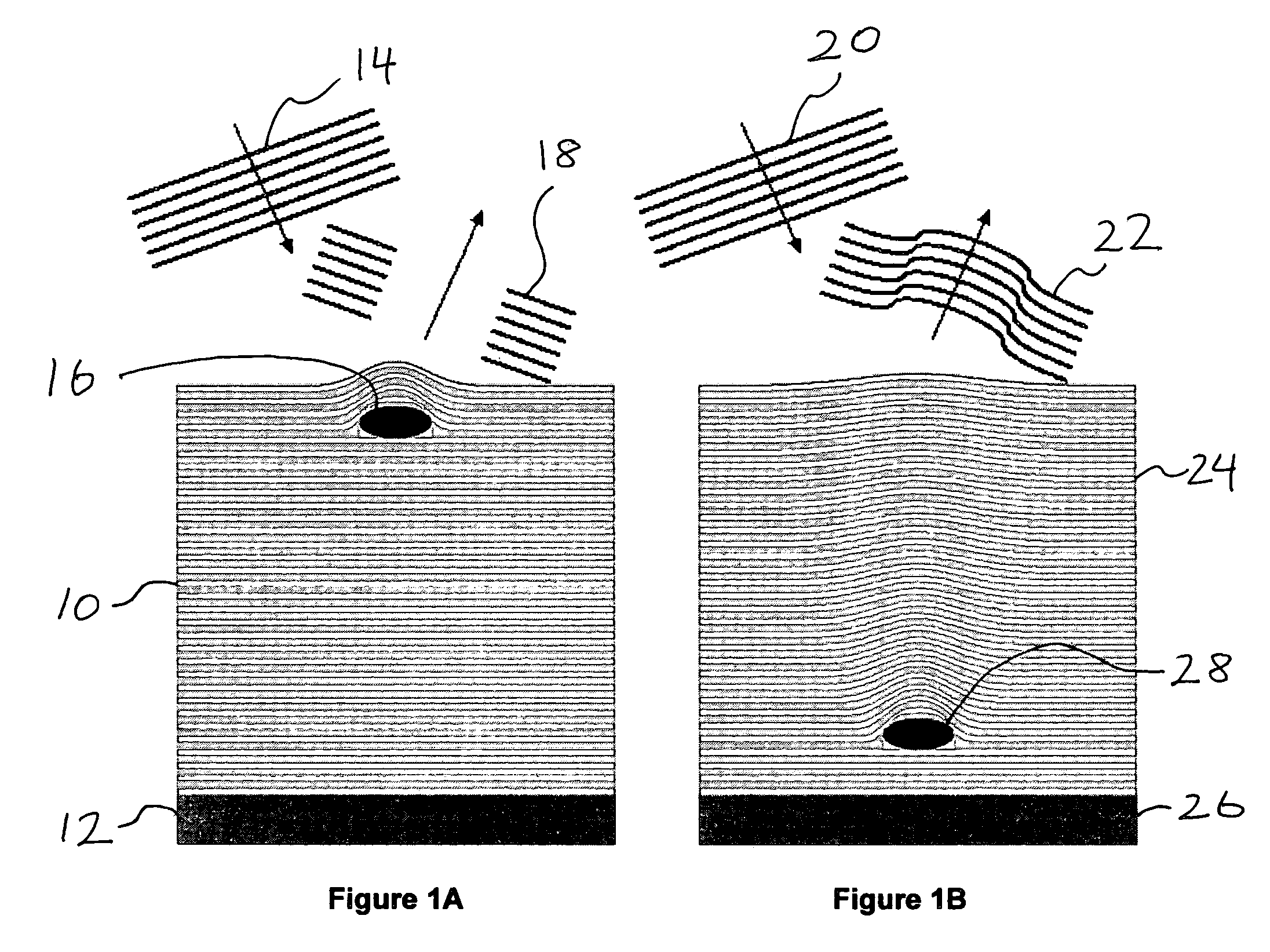
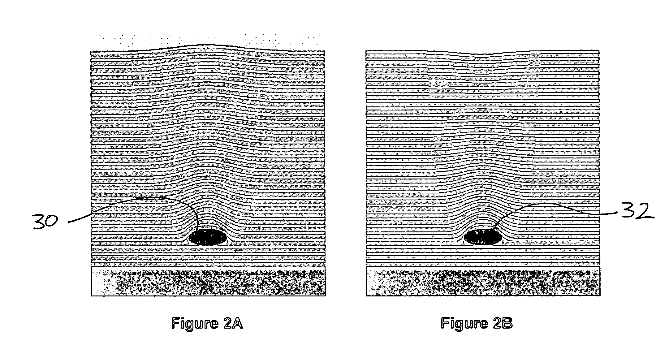
The fundamental physics of EUV lithography creates unique challenges when applied to HAR structures. The 13.5nm wavelength of EUV light introduces complex interactions with photoresist materials, resulting in stochastic effects that become more pronounced in HAR patterns. These stochastic variations manifest as line edge roughness (LER), line width roughness (LWR), and critical dimension uniformity (CDU) issues that are particularly problematic as aspect ratios increase beyond 5:1.
Pattern collapse represents one of the most significant challenges in HAR EUV patterning. As aspect ratios increase, capillary forces during the development and drying processes can cause adjacent features to bend and touch, resulting in complete pattern failure. This phenomenon becomes exponentially more severe with increasing aspect ratios, creating a practical ceiling for achievable dimensions.
Material limitations further complicate HAR EUV implementation. Current photoresist formulations struggle to provide the combination of high sensitivity, low outgassing, sufficient etch resistance, and mechanical stability required for HAR patterning. The trade-off between resolution and sensitivity—often referred to as the "RLS triangle"—becomes particularly constraining when attempting to create stable HAR structures.
Etch transfer processes face significant hurdles when working with HAR patterns. The directional precision required to maintain vertical sidewalls through the entire depth of high-aspect-ratio features demands unprecedented control over plasma parameters, ion energies, and chemical selectivity. Aspect-ratio-dependent etching (ARDE) effects become more pronounced, leading to non-uniform feature depths and profile variations.
Metrology and inspection capabilities are stretched to their limits with HAR EUV patterns. Traditional techniques struggle to accurately measure and characterize deep, narrow features, creating challenges for process control and defect detection. The industry faces a critical gap in its ability to "see" what is happening at the bottom of HAR structures, complicating efforts to optimize processes.
Integration challenges multiply when HAR EUV patterns must be incorporated into complex 3D device architectures. The precise alignment required between multiple HAR layers, combined with the mechanical stresses introduced by subsequent processing steps, creates yield-limiting issues that must be addressed through holistic process development approaches rather than isolated optimizations.
Current Defect Mitigation Techniques
01 EUV lithography pattern defect detection and inspection
Various methods and systems for detecting and inspecting defects in high-aspect-ratio EUV patterns. These include advanced optical inspection tools, electron beam inspection systems, and scatterometry techniques that can identify pattern irregularities, bridging defects, and line edge roughness in EUV lithography. These inspection methods are crucial for maintaining quality control in semiconductor manufacturing processes using extreme ultraviolet lithography.- EUV lithography process optimization for high-aspect-ratio patterns: Optimizing the EUV lithography process is crucial for creating high-aspect-ratio patterns with minimal defects. This includes adjusting exposure parameters, developing specialized resists, and implementing precise pattern transfer techniques. Advanced process control methods help maintain critical dimensions and reduce pattern collapse in high-aspect-ratio structures, resulting in improved yield and performance of semiconductor devices.
- Defect inspection and metrology for EUV patterning: Advanced inspection and metrology techniques are essential for detecting and characterizing defects in high-aspect-ratio EUV patterns. These methods include electron microscopy, optical inspection systems, and scatterometry that can identify pattern irregularities, line edge roughness, and other defects at nanometer scales. Real-time monitoring during fabrication allows for immediate process adjustments to minimize defect propagation.
- Materials engineering for defect reduction in EUV lithography: Specialized materials are developed to address defect challenges in high-aspect-ratio EUV patterning. This includes advanced photoresist formulations with enhanced sensitivity and contrast, anti-reflective coatings that minimize standing waves, and underlayer materials that improve adhesion and pattern transfer. These materials are designed to withstand the high energy of EUV radiation while maintaining pattern fidelity and reducing defect formation.
- Post-lithography treatments for defect mitigation: Various post-lithography treatments can be applied to reduce defects in high-aspect-ratio EUV patterns. These include plasma treatments to smooth sidewalls, annealing processes to reduce line edge roughness, and specialized cleaning techniques to remove residual particles without damaging delicate features. Chemical rinse processes and surface modification treatments help stabilize high-aspect-ratio structures and prevent pattern collapse during subsequent processing steps.
- Integration of computational methods for defect prediction and control: Computational methods play a critical role in predicting and controlling defects in high-aspect-ratio EUV patterns. Advanced modeling and simulation tools help optimize mask designs, predict process windows, and identify potential defect sources before manufacturing. Machine learning algorithms analyze process data to detect patterns that lead to defects, enabling proactive adjustments. These computational approaches reduce development time and improve yield for complex high-aspect-ratio structures.
02 Resist formulations for high-aspect-ratio EUV patterning
Specialized photoresist formulations designed specifically for EUV lithography that enable the creation of high-aspect-ratio patterns while minimizing defects. These formulations include additives that improve sensitivity to EUV radiation, enhance pattern resolution, reduce line edge roughness, and prevent pattern collapse in high-aspect-ratio structures. The chemical composition of these resists is optimized to achieve better pattern fidelity and defect control.Expand Specific Solutions03 Post-exposure processing techniques for defect reduction
Various post-exposure processing methods that help reduce defects in high-aspect-ratio EUV patterns. These include specialized development processes, rinse techniques, and drying methods that prevent pattern collapse and minimize residual defects. Additional treatments such as plasma etching optimization, surface treatments, and annealing processes can further enhance pattern quality and reduce defect density in critical high-aspect-ratio structures.Expand Specific Solutions04 Multi-patterning and integration strategies
Advanced patterning strategies that combine EUV lithography with complementary techniques to achieve high-aspect-ratio structures while controlling defects. These include directed self-assembly, multi-patterning approaches, and hybrid lithography schemes. Such integration strategies help overcome the limitations of single-exposure EUV lithography and enable the creation of complex high-aspect-ratio patterns with reduced defect rates and improved dimensional control.Expand Specific Solutions05 Mask design and optimization for defect mitigation
Specialized EUV mask design approaches that help minimize pattern defects in high-aspect-ratio structures. These include optical proximity correction techniques, assist features, and phase-shifting elements that improve image fidelity. Advanced computational methods for mask optimization help predict and prevent common defect types in high-aspect-ratio patterns. Proper mask maintenance and handling procedures also contribute significantly to defect reduction.Expand Specific Solutions
Leading Semiconductor Equipment and Materials Providers
The EUV defect control market for high-aspect-ratio patterns is currently in a growth phase, with an estimated market size exceeding $5 billion annually. The technology maturity varies across different solution segments, with inspection tools more advanced than prevention technologies. Leading players include ASML Netherlands BV as the dominant EUV lithography equipment provider, while KLA TENCOR and Applied Materials lead in metrology and inspection solutions. Taiwan Semiconductor Manufacturing Co. (TSMC) and Samsung Electronics are driving implementation as primary end-users, with significant R&D investments. Carl Zeiss SMT contributes critical optical components for EUV systems. The competitive landscape shows regional strengths with Western companies (ASML, KLA) leading in equipment development while Asian manufacturers (TSMC, Samsung, SK hynix) focus on implementation and process optimization.
Taiwan Semiconductor Manufacturing Co., Ltd.
Technical Solution: TSMC has developed a multi-faceted approach to defect control in high-aspect-ratio EUV patterns, focusing on both process optimization and material engineering. Their strategy includes a proprietary resist formulation specifically designed to minimize pattern collapse in high-aspect-ratio features by optimizing polymer chain length distribution and incorporating novel cross-linking agents. TSMC employs advanced computational modeling to predict and mitigate stochastic effects in EUV patterning, using machine learning algorithms to identify optimal process windows for different pattern geometries. Their approach incorporates specialized post-exposure bake (PEB) protocols with precisely controlled temperature gradients to reduce line edge roughness while maintaining structural integrity. TSMC has also pioneered innovative development techniques using customized surfactants and controlled drying methods to prevent pattern collapse during the critical rinse and dry steps. Additionally, they implement comprehensive in-line metrology with automated defect classification systems that enable rapid process corrections and continuous improvement of their high-aspect-ratio patterning capabilities.
Strengths: Industry-leading manufacturing expertise with proven high-volume production capabilities; extensive process integration knowledge across multiple technology nodes; proprietary materials and process recipes optimized for specific device architectures. Weaknesses: Highly customized solutions may limit transferability across different product types; significant capital investment requirements for continuous technology advancement; complex process control systems require specialized engineering talent.
KLA TENCOR CORP
Technical Solution: KLA's approach to defect control in high-aspect-ratio EUV patterns focuses on advanced inspection and metrology solutions. Their strategy centers on their proprietary broadband plasma illumination technology that enables high-sensitivity detection of defects in deep, narrow structures that traditional optical systems cannot resolve. KLA has developed specialized algorithms for their e-beam inspection systems that can identify subtle pattern deformations and bridging defects in high-aspect-ratio features with dimensions below 20nm. Their comprehensive solution includes advanced machine learning techniques that automatically classify defects and correlate them with specific process parameters, enabling rapid root cause analysis and process optimization. KLA's metrology systems incorporate unique 3D profile measurement capabilities that can accurately characterize sidewall angles and line edge roughness in high-aspect-ratio structures, providing critical feedback for process control. Additionally, they've implemented hybrid metrology approaches that combine optical, e-beam, and X-ray techniques to provide complementary data sets that enhance defect detection sensitivity and measurement accuracy in challenging high-aspect-ratio patterns.
Strengths: Industry-leading inspection and metrology technology specifically optimized for EUV lithography; comprehensive data analytics capabilities that enable sophisticated process control; vendor-neutral position allowing integration with diverse manufacturing environments. Weaknesses: Focus primarily on detection rather than prevention of defects; limited direct control over process improvements; solutions require significant computational resources and specialized expertise to implement effectively.
Critical Patents in EUV Defect Control
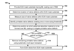
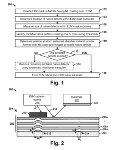
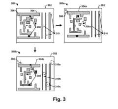
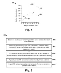
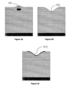
Efficient solution for removing EUV native defects
PatentActiveUS20160282713A1
Innovation
- A method involving the measurement and identification of native defects in EUV mask substrates, followed by the strategic placement of a patterned absorber material to hide defects and a systematic multi-layer transplant procedure using dry etching to replace defective sections with defect-free layers, thereby minimizing the impact of printable native defects on the EUV lithography process.
Method for characterizing mask defects using image reconstruction from X-ray diffraction patterns
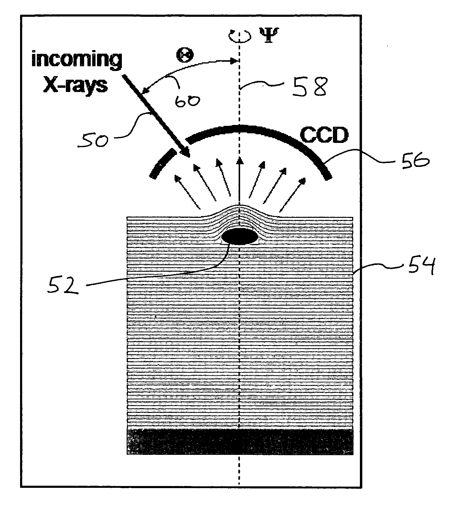
PatentInactiveUS20050185173A1
Innovation
- A method using image reconstruction from X-ray diffraction patterns to create three-dimensional images of defects, allowing for the selection of appropriate repair techniques, combined with localized energy deposition techniques like focused electron beams to correct defects with high spatial resolution.
Yield Impact Analysis and Economic Considerations
The economic impact of defects in high-aspect-ratio EUV patterns extends far beyond technical considerations, directly affecting semiconductor manufacturing yields and overall production economics. Yield losses attributed to pattern defects can range from 5% to 20% depending on process maturity, with high-aspect-ratio features being particularly susceptible to yield degradation. Financial analysis indicates that for a typical 300mm wafer fabrication facility, each percentage point of yield loss translates to approximately $1-2 million in lost revenue annually per product line.
Defect density metrics reveal that EUV-specific defects contribute significantly to yield limitations, with current industry benchmarks showing 0.1-0.2 critical defects per square centimeter for mature processes. However, when dealing with high-aspect-ratio patterns, these figures can deteriorate to 0.3-0.5 defects per square centimeter, creating substantial economic pressure on manufacturers.
Cost modeling of defect control strategies demonstrates a complex return-on-investment landscape. Implementation of advanced inspection tools for high-aspect-ratio patterns typically requires capital expenditure of $10-15 million per tool, while process optimization techniques may demand $3-5 million in development costs. These investments must be balanced against the projected yield improvements, with most tier-one semiconductor manufacturers requiring payback periods under 18 months to justify implementation.
The economic equation becomes more nuanced when considering opportunity costs. Production delays resulting from defect-related issues in high-aspect-ratio patterns can postpone time-to-market by 3-6 months for new semiconductor products, potentially resulting in market share losses of 5-10% in fast-moving segments like mobile processors or memory chips.
Risk assessment frameworks indicate that defect control strategies should be prioritized based on their yield impact coefficient—a metric combining defect probability, detection difficulty, and economic consequence. For high-aspect-ratio EUV patterns, line collapse and bridging defects typically score highest on this coefficient, justifying more aggressive investment in their prevention and detection.
Long-term economic modeling suggests that systematic investment in defect control capabilities for high-aspect-ratio patterns delivers compound benefits, as knowledge and techniques developed for current nodes become foundational for future technology generations. This creates a virtuous cycle where early adopters of robust defect control strategies gain sustainable competitive advantages through consistently higher yields and faster technology transitions.
Metrology Advancements for Defect Detection
The evolution of metrology tools for defect detection in high-aspect-ratio EUV patterns has accelerated significantly in recent years. Traditional optical inspection methods face fundamental limitations when dealing with sub-10nm features, necessitating the development of advanced metrology solutions. Electron-beam based inspection systems have emerged as critical tools, with high-resolution scanning electron microscopy (SEM) and transmission electron microscopy (TEM) offering nanometer-scale defect detection capabilities essential for EUV lithography quality control.
Multi-beam electron inspection systems represent a significant advancement, enabling parallel inspection processes that dramatically improve throughput while maintaining sensitivity to critical defects. These systems can detect bridging defects, line breaks, and pattern collapse in high-aspect-ratio structures that would be invisible to conventional optical systems.
Actinic inspection tools utilizing EUV wavelengths (13.5nm) have shown promising results in detecting phase defects and subtle pattern irregularities specific to EUV processes. Though still in development stages at leading equipment manufacturers, these tools address the unique challenges of EUV-specific defect modes that other inspection methods might miss.
Machine learning algorithms have been integrated into metrology workflows, enhancing defect classification accuracy and reducing false positives. Deep learning models trained on extensive defect libraries can now distinguish between critical and non-critical defects in complex 3D structures, significantly improving decision-making in high-volume manufacturing environments.
In-line metrology solutions have evolved to provide real-time feedback during the manufacturing process. Advanced scatterometry and optical critical dimension (OCD) techniques, when combined with sophisticated modeling algorithms, enable non-destructive measurements of sidewall angles and feature dimensions in high-aspect-ratio structures. This allows for immediate process corrections before defects propagate through subsequent manufacturing steps.
Hybrid metrology approaches, combining multiple measurement techniques, have demonstrated superior accuracy in characterizing complex defect types. By correlating data from complementary techniques such as atomic force microscopy (AFM), X-ray metrology, and electron-based imaging, engineers can obtain comprehensive defect profiles that would be impossible with any single method.
The integration of metrology systems into unified data platforms represents another significant advancement. These platforms enable correlation between different inspection points in the manufacturing process, facilitating root cause analysis and predictive defect prevention strategies essential for maintaining yield in advanced EUV processes.
Unlock deeper insights with PatSnap Eureka Quick Research — get a full tech report to explore trends and direct your research. Try now!
Generate Your Research Report Instantly with AI Agent
Supercharge your innovation with PatSnap Eureka AI Agent Platform!