

Solvent Development for Enhanced EUV Pattern Transfer
OCT 13, 20259 MIN READ
Generate Your Research Report Instantly with AI Agent
PatSnap Eureka helps you evaluate technical feasibility & market potential.
EUV Lithography Solvent Background and Objectives
Extreme Ultraviolet (EUV) lithography represents a revolutionary advancement in semiconductor manufacturing, enabling the production of increasingly miniaturized integrated circuits with feature sizes below 7nm. The development of appropriate solvents for EUV lithography processes has become a critical factor in achieving optimal pattern transfer and maintaining the integrity of increasingly complex semiconductor structures.
The evolution of lithography technology has progressed from deep ultraviolet (DUV) using 193nm wavelength light to EUV at 13.5nm wavelength, representing a significant leap in resolution capabilities. This transition has necessitated a complete reimagining of the photoresist chemistry and associated solvent systems to accommodate the unique photochemical mechanisms triggered by high-energy EUV photons.
Traditional solvents used in DUV lithography often prove inadequate for EUV processes due to different dissolution behaviors, interaction with novel photoresist materials, and compatibility requirements with increasingly complex multi-layer stacks. The technical objective of solvent development for EUV lithography centers on creating formulations that enable precise pattern definition while minimizing pattern collapse, line edge roughness, and defectivity.
Key objectives in EUV solvent development include achieving enhanced dissolution selectivity between exposed and unexposed regions, minimizing swelling of photoresist features, reducing surface tension effects that contribute to pattern collapse, and ensuring compatibility with both the photoresist chemistry and underlying substrate materials. Additionally, environmental considerations and worker safety concerns are driving research toward greener solvent alternatives with reduced toxicity and environmental impact.
The historical trajectory of solvent development has seen a shift from simple single-component systems to sophisticated multi-component formulations designed to fine-tune the development process. Recent advances have focused on custom-designed solvent mixtures that can selectively interact with specific chemical moieties in EUV photoresists, enabling unprecedented control over the development process.
Current research aims to address the unique challenges posed by EUV lithography, including the need for solvents that can effectively develop high-absorption photoresists, manage outgassing concerns, and maintain compatibility with vacuum environments often used in EUV exposure systems. The ultimate goal is to develop solvent systems that enable the theoretical resolution limits of EUV lithography to be realized in high-volume manufacturing environments.
As the semiconductor industry continues its relentless pursuit of Moore's Law, the development of specialized solvents for EUV lithography represents a critical enabling technology that will determine the pace and extent of future miniaturization capabilities in integrated circuit manufacturing.
Market Analysis for Advanced Semiconductor Patterning Solutions
The global market for advanced semiconductor patterning solutions is experiencing robust growth, driven by the continuous miniaturization of semiconductor devices and the increasing adoption of extreme ultraviolet (EUV) lithography technology. As of 2023, the semiconductor equipment market reached approximately $107 billion, with lithography tools accounting for nearly 30% of this value. Within this segment, EUV-related materials and processes represent one of the fastest-growing subsectors.
The demand for specialized solvents for EUV pattern transfer is primarily fueled by the semiconductor manufacturing industry's push toward 5nm, 3nm, and even 2nm process nodes. Major semiconductor manufacturers including TSMC, Samsung, and Intel have announced significant capital expenditures for EUV lithography implementation, with combined investments exceeding $200 billion over the next five years.
Regionally, East Asia dominates the market with Taiwan, South Korea, and Japan collectively accounting for over 65% of the global demand for advanced patterning solutions. North America represents approximately 20% of the market, while Europe contributes around 12%. The remaining market share is distributed across emerging semiconductor manufacturing regions.
The solvent development segment for EUV pattern transfer is projected to grow at a compound annual growth rate (CAGR) of 14.8% through 2028, outpacing the broader semiconductor materials market. This growth is attributed to the critical role these specialized solvents play in achieving the resolution, sensitivity, and line edge roughness requirements of next-generation semiconductor devices.
Customer segments for advanced patterning solutions include foundries (48% of market demand), memory manufacturers (32%), and integrated device manufacturers (20%). The foundry segment, led by TSMC and Samsung, is expected to maintain the highest growth rate due to their aggressive EUV implementation roadmaps.
Key market drivers include the increasing complexity of semiconductor designs, growing demand for high-performance computing applications, and the expansion of 5G infrastructure. Additionally, emerging applications in artificial intelligence, autonomous vehicles, and Internet of Things (IoT) devices are creating new demand vectors for advanced semiconductor components that require precise patterning solutions.
Market challenges include the high cost of EUV implementation, technical difficulties in pattern transfer at sub-7nm nodes, and supply chain vulnerabilities for specialized materials. Environmental regulations regarding solvent usage and disposal also present compliance challenges for market participants, particularly in Europe and North America.
Current Solvent Technologies and Challenges in EUV Lithography
The current landscape of solvents in EUV lithography represents a critical component in the semiconductor manufacturing process. Traditional solvents such as propylene glycol methyl ether acetate (PGMEA), cyclohexanone, and ethyl lactate have been widely utilized in conventional lithography processes. However, with the transition to EUV lithography, these conventional solvents face significant limitations due to the unique requirements of EUV resist systems.
EUV lithography operates at an extremely short wavelength of 13.5 nm, which introduces new challenges for solvent performance. The primary challenge lies in achieving optimal dissolution selectivity between exposed and unexposed regions of the photoresist. Current solvents struggle to maintain this selectivity at the nanoscale dimensions required for EUV processes, often resulting in pattern collapse or insufficient development contrast.
Another significant challenge is the compatibility between solvents and the complex multi-layer resist systems used in EUV lithography. These systems often incorporate metal-containing components and novel polymer architectures that interact differently with conventional solvents. The chemical interactions between these advanced materials and traditional solvents can lead to residue formation, line edge roughness, and degraded pattern fidelity.
Environmentally friendly solvents represent another area of active development. Traditional semiconductor solvents often contain volatile organic compounds (VOCs) with significant environmental impacts. The industry is increasingly seeking greener alternatives that maintain performance while reducing environmental footprint, though these eco-friendly options frequently demonstrate reduced effectiveness in critical EUV parameters.
Temperature sensitivity presents an additional challenge, as EUV processes require precise thermal control during development. Current solvents exhibit varying degrees of temperature-dependent performance, which can impact process windows and manufacturing consistency. Some advanced facilities have implemented temperature-controlled development systems, but the fundamental solvent properties remain a limiting factor.
Recent innovations have explored binary and ternary solvent systems that combine different solvents to achieve enhanced performance characteristics. These mixed systems show promise in addressing some challenges but introduce complexity in process control and qualification. Additionally, supercritical CO2 and other alternative development media have been investigated as potential replacements for traditional liquid solvents, though they require significant modifications to existing equipment infrastructure.
The integration of these solvent technologies with automated track systems presents further challenges, as flow dynamics, nozzle designs, and puddle time optimization must all be recalibrated for new solvent properties. This integration complexity often slows the adoption of novel solvent technologies in high-volume manufacturing environments.
Current Solvent Formulations for EUV Pattern Transfer
01 Solvent-based pattern transfer techniques in semiconductor manufacturing
Solvent-based pattern transfer methods are used in semiconductor fabrication to create precise microstructures. These techniques involve using specific solvents to dissolve or soften selected areas of a resist layer, allowing for the transfer of patterns onto semiconductor substrates. The process typically includes applying a resist material, exposing it to create a pattern, and then using solvents for development. This approach enables high-resolution pattern transfer essential for manufacturing advanced integrated circuits and microelectronic devices.- Solvent-based pattern transfer techniques in semiconductor manufacturing: Solvent-based pattern transfer methods are used in semiconductor fabrication to create precise microstructures. These techniques involve using specific solvents to dissolve or modify selected areas of photoresist or other materials, allowing for the transfer of patterns onto substrates. The process typically includes applying a resist layer, exposing it to radiation through a mask, and then developing the pattern using appropriate solvents that selectively remove portions of the material.
- Solvent selection for pattern transfer optimization: The choice of solvent significantly impacts the quality and resolution of pattern transfer. Different solvents offer varying dissolution rates, selectivity, and compatibility with substrate materials. Optimized solvent systems can enhance pattern fidelity, reduce defects, and improve overall transfer efficiency. Factors considered in solvent selection include volatility, surface tension, viscosity, and environmental impact, all of which affect the final pattern quality and process reliability.
- Multilayer solvent transfer processes: Multilayer solvent transfer processes involve the sequential application and patterning of different material layers using various solvents. This approach allows for complex three-dimensional structures to be created with high precision. Each layer may require specific solvent treatments to achieve the desired pattern transfer while maintaining compatibility with underlying layers. These techniques are particularly valuable in creating advanced microelectronic devices, optical components, and specialized surfaces with tailored properties.
- Environmentally friendly solvent systems for pattern transfer: Development of eco-friendly solvent systems addresses environmental and health concerns associated with traditional pattern transfer processes. These green alternatives reduce toxic emissions, minimize waste generation, and decrease worker exposure to hazardous chemicals. Approaches include using bio-based solvents, water-based systems, supercritical fluids, and ionic liquids that maintain or improve pattern transfer performance while reducing environmental impact. These sustainable solutions are becoming increasingly important as manufacturing regulations become more stringent.
- Novel applications of solvent pattern transfer: Beyond traditional semiconductor manufacturing, solvent pattern transfer techniques have expanded to diverse applications including flexible electronics, biomedical devices, optical components, and advanced materials. These methods enable the creation of functional surfaces with controlled wettability, adhesion, and optical properties. The versatility of solvent-based approaches allows for patterning on unconventional substrates such as polymers, textiles, and biological materials, opening new possibilities for innovative product development across multiple industries.
02 Solvent selection for optimal pattern transfer
The choice of solvent significantly impacts the quality and precision of pattern transfer processes. Different solvents offer varying dissolution rates, selectivity, and compatibility with resist materials. Factors such as solvent polarity, volatility, and viscosity affect pattern resolution, edge definition, and overall transfer fidelity. Optimized solvent systems may include mixtures of multiple solvents to achieve desired properties. Proper solvent selection helps minimize pattern distortion, improve feature resolution, and enhance the overall efficiency of the transfer process.Expand Specific Solutions03 Environmentally friendly solvent transfer methods
Recent developments in solvent pattern transfer focus on environmentally sustainable approaches that reduce the use of hazardous chemicals. These methods employ biodegradable solvents, water-based systems, or supercritical fluids as alternatives to traditional organic solvents. Such eco-friendly techniques minimize environmental impact while maintaining high-quality pattern transfer. Additionally, these methods often reduce worker exposure to harmful substances and decrease waste disposal challenges, making the manufacturing process more sustainable without compromising performance.Expand Specific Solutions04 Advanced solvent-assisted nanoimprint lithography
Solvent-assisted nanoimprint lithography combines traditional imprinting techniques with solvent-based processes to achieve high-resolution pattern transfer at the nanoscale. This method uses solvents to soften polymer resist materials, allowing for more efficient mold filling and pattern replication. The technique enables the creation of complex three-dimensional nanostructures with precise control over feature dimensions. By optimizing solvent parameters such as concentration and exposure time, this approach achieves enhanced pattern fidelity while reducing the pressure and temperature requirements of conventional nanoimprint processes.Expand Specific Solutions05 Solvent vapor annealing for pattern enhancement
Solvent vapor annealing is a technique used to improve pattern quality by exposing patterned substrates to controlled solvent vapor environments. This process allows polymer chains in the pattern to reorganize and self-assemble, resulting in smoother surfaces, reduced defects, and enhanced pattern definition. The method is particularly valuable for block copolymer lithography and other self-assembly-based patterning approaches. By carefully controlling parameters such as vapor concentration, exposure time, and temperature, this technique can significantly improve pattern resolution and structural integrity without damaging the underlying features.Expand Specific Solutions
Leading Companies in EUV Solvent Development
The EUV solvent development market is in a growth phase, with increasing demand driven by advanced semiconductor manufacturing needs. Key players include JSR Corp., Tokyo Electron, and DuPont, who are leading innovation in this specialized chemical segment. ASML, as the primary EUV lithography equipment provider, shapes market requirements while semiconductor manufacturers like Samsung, TSMC, and GlobalFoundries drive adoption. The technology is approaching maturity for current nodes but continues evolving for sub-3nm processes. Chemical companies including AGC, FUJIFILM, and YCCHEM are developing specialized formulations to address pattern collapse and line edge roughness challenges, while equipment manufacturers like Lam Research and Applied Materials integrate these solutions into their process flows.
JSR Corp.
Technical Solution: JSR Corporation has developed advanced EUV resist materials specifically designed for enhanced pattern transfer in extreme ultraviolet lithography. Their technology focuses on metal-oxide resist platforms that offer high sensitivity and low line edge roughness (LER). JSR's EUV resist solutions incorporate unique molecular design with controlled acid diffusion mechanisms to achieve superior resolution below 20nm. The company has pioneered hybrid resist systems combining organic and inorganic components to balance sensitivity and resolution requirements. Their latest generation of EUV resists features specialized polymeric structures with optimized protecting groups that respond efficiently to EUV radiation while maintaining pattern fidelity. JSR has also developed complementary rinse materials and topcoat solutions that work synergistically with their resists to prevent pattern collapse and improve process latitude[1][3].
Strengths: Superior resolution capability below 20nm with excellent pattern fidelity; optimized acid diffusion control for enhanced sensitivity-resolution balance; comprehensive material ecosystem including rinse solutions. Weaknesses: Higher cost compared to traditional resist systems; may require specialized processing equipment; performance can be substrate-dependent requiring additional optimization.
DuPont de Nemours, Inc.
Technical Solution: DuPont has developed a comprehensive EUV solvent platform focused on environmentally sustainable solutions for next-generation semiconductor manufacturing. Their approach centers on novel green solvents with reduced environmental impact while maintaining high performance in EUV lithography processes. DuPont's technology incorporates specially engineered solvent blends that optimize dissolution properties for EUV resists while minimizing swelling and pattern collapse. Their solvent systems feature controlled evaporation rates tailored for specific process steps, from resist coating to development and rinsing. DuPont has also pioneered advanced developer solutions with tuned Hansen solubility parameters that enhance contrast between exposed and unexposed regions of EUV resists. Additionally, their portfolio includes specialized post-development rinse solutions designed to remove residual contaminants while preserving pattern integrity down to sub-10nm features[2][5].
Strengths: Industry-leading environmental sustainability profile; comprehensive solvent ecosystem covering all process steps; excellent compatibility with diverse resist platforms. Weaknesses: May require process modifications when transitioning from traditional solvents; higher initial cost compared to conventional options; performance optimization needed for specific resist chemistries.
Key Patents and Research in EUV-Compatible Solvents
Method for extreme ultraviolet (EUV) resist patterning development
PatentPendingJP2023549608A
Innovation
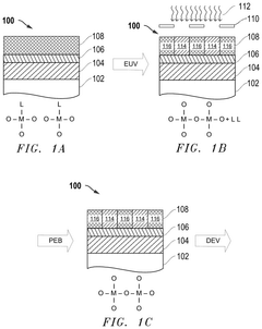
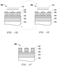
- A novel plasma-based process for patterning metal oxide photoresists involves exposing the resist to EUV light, separating organic ligands, followed by a bake process and iterative plasma etching steps using hydrocarbon or fluorocarbon-based plasmas for deposition and hydrogen or halogen-based plasmas for etching, to create precise patterns.
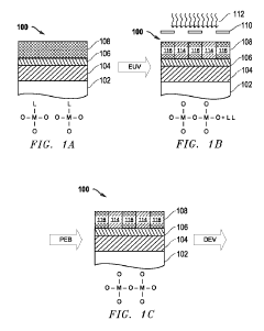
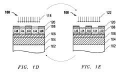
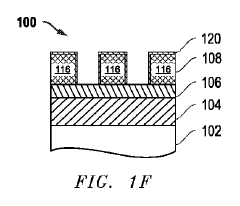
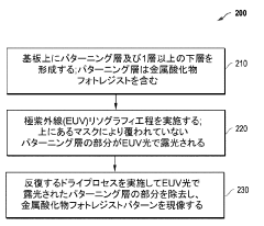
Methods for Extreme Ultraviolet (EUV) Resist Patterning Development
PatentPendingUS20250076771A1
Innovation
- A novel process flow and method for patterning metal-oxide photoresists using EUV or lower wavelength light, which involves forming a patterning layer, exposing it to EUV light to separate organic ligands from metal-oxide structures, followed by a bake process and a cyclic dry plasma process to develop the pattern.
Environmental Impact and Sustainability of EUV Solvents
The environmental impact of solvents used in Extreme Ultraviolet (EUV) lithography processes represents a critical consideration for semiconductor manufacturing sustainability. Traditional lithographic solvents often contain volatile organic compounds (VOCs) that contribute significantly to air pollution, ozone depletion, and greenhouse gas emissions. As EUV technology adoption accelerates across the semiconductor industry, the environmental footprint of these specialized solvents demands urgent attention.
Current EUV solvent systems frequently utilize perfluorinated compounds (PFCs) and other persistent chemicals that resist natural degradation. These substances can remain in ecosystems for decades, bioaccumulating in wildlife and potentially entering human food chains. Studies indicate that some EUV process solvents demonstrate half-lives exceeding 1,000 years in certain environmental conditions, presenting long-term ecological concerns.
Water consumption represents another significant sustainability challenge. EUV lithography typically requires ultra-pure water for rinsing processes, with a single fabrication facility potentially consuming millions of gallons daily. This intensive water usage creates substantial pressure on local water resources, particularly in semiconductor manufacturing hubs experiencing water scarcity.
Recent regulatory frameworks, including the European Union's REACH (Registration, Evaluation, Authorization and Restriction of Chemicals) and various global initiatives to reduce perfluoroalkyl substances (PFAS), are increasingly targeting chemicals common in EUV processes. These regulatory pressures are driving innovation toward greener alternatives that maintain technical performance while reducing environmental impact.
Promising sustainable approaches include the development of bio-based solvents derived from renewable feedstocks. Research indicates that modified terpenes and other plant-derived compounds can achieve pattern transfer quality comparable to conventional solvents while offering enhanced biodegradability. Additionally, supercritical CO2 systems show potential as environmentally benign alternatives, utilizing recaptured carbon dioxide as a processing medium.
Closed-loop solvent recovery systems represent another sustainability advancement, with modern facilities implementing sophisticated distillation and filtration technologies that can reclaim up to 90% of process solvents. These systems significantly reduce both waste generation and virgin material requirements, though energy consumption during recovery processes remains a challenge requiring optimization.
Life cycle assessment (LCA) methodologies are increasingly being applied to EUV solvent selection, enabling comprehensive evaluation of environmental impacts from raw material extraction through manufacturing and ultimate disposal. This holistic approach helps identify unexpected environmental trade-offs and guides development toward truly sustainable solutions rather than merely shifting environmental burdens between different impact categories.
Integration Challenges with Existing Semiconductor Processes
The integration of EUV solvent development processes into existing semiconductor manufacturing workflows presents significant challenges that require careful consideration. Current semiconductor fabrication lines are optimized for traditional lithography techniques, and the introduction of EUV-specific solvents necessitates substantial modifications to established processes.
One primary integration challenge is compatibility with existing equipment. Many semiconductor fabs have invested heavily in tools designed for 193nm immersion lithography, and retrofitting these systems for EUV-compatible solvents can be costly and complex. The solvent delivery systems, waste management infrastructure, and environmental controls may all require upgrades to handle the unique properties of EUV-specific development solvents.
Material compatibility issues also emerge when introducing new solvents into established process flows. EUV-optimized solvents must not adversely interact with other materials used in the semiconductor manufacturing process, including photoresists, anti-reflective coatings, and various metals and dielectrics. Cross-contamination risks must be thoroughly evaluated and mitigated to prevent yield losses.
Temperature sensitivity presents another significant integration hurdle. Many EUV solvents exhibit optimal performance within narrow temperature ranges, requiring precise thermal management throughout the development process. Existing fab temperature control systems may need enhancement to maintain the tight tolerances necessary for consistent EUV pattern development.
Process timing and throughput considerations further complicate integration efforts. EUV solvent development steps may require different development times compared to traditional processes, potentially creating bottlenecks in high-volume manufacturing environments. Balancing development quality against production throughput remains a critical challenge for semiconductor manufacturers.
Environmental, health, and safety (EHS) compliance represents yet another integration challenge. New EUV solvents must meet increasingly stringent regulations regarding volatile organic compounds (VOCs), greenhouse gas emissions, and worker exposure limits. Existing exhaust, containment, and monitoring systems may require significant modifications to accommodate these specialized chemicals.
Finally, metrology and quality control systems must be adapted to effectively monitor the performance of EUV solvent development processes. Existing inspection tools may require recalibration or replacement to accurately detect the unique defect signatures associated with EUV pattern transfer, ensuring that integration challenges do not compromise final device quality or reliability.
Unlock deeper insights with PatSnap Eureka Quick Research — get a full tech report to explore trends and direct your research. Try now!
Generate Your Research Report Instantly with AI Agent
Supercharge your innovation with PatSnap Eureka AI Agent Platform!