Thermal Stability of Photoresist Polymers under EUV Exposure
OCT 13, 20259 MIN READ
Generate Your Research Report Instantly with AI Agent
Patsnap Eureka helps you evaluate technical feasibility & market potential.
EUV Photoresist Evolution and Objectives
Extreme Ultraviolet (EUV) lithography represents a revolutionary advancement in semiconductor manufacturing, enabling the production of increasingly miniaturized integrated circuits with feature sizes below 7nm. The evolution of EUV photoresist technology has been marked by significant milestones over the past two decades, transitioning from conceptual research to commercial implementation.
The journey began in the early 2000s with the exploration of chemically amplified resists (CARs) adapted from 193nm lithography. These early materials faced fundamental limitations in resolution and sensitivity when exposed to 13.5nm EUV radiation. By 2010, dedicated EUV resist platforms emerged, focusing on higher absorption cross-sections and improved acid generation efficiency.
A critical turning point occurred between 2015-2018 when metal-oxide based resists were introduced, offering substantially improved sensitivity and addressing the notorious "RLS triangle" trade-off between resolution, line-edge roughness, and sensitivity. This innovation enabled the first commercial EUV lithography deployments in high-volume manufacturing environments.
Current development focuses on addressing thermal stability challenges that manifest during EUV exposure. The high-energy photons (91.6 eV) generate not only the desired photochemical reactions but also significant thermal effects that can compromise pattern fidelity. Research indicates that localized heating can reach 100-300°C within nanoseconds, potentially causing polymer degradation, outgassing, and pattern collapse.
The primary technical objective is to develop photoresist polymers with enhanced thermal stability that maintain structural integrity under intense EUV radiation while preserving high resolution capabilities. Specifically, the industry aims to achieve sub-10nm half-pitch resolution with line edge roughness below 2nm and sensitivity better than 30 mJ/cm².
Secondary objectives include reducing outgassing during exposure to prevent contamination of expensive EUV optics, improving etch resistance to support subsequent processing steps, and enhancing mechanical stability to prevent pattern collapse at extreme dimensions.
Looking forward, the technology roadmap targets photoresist materials capable of supporting 3nm and below process nodes by 2025. This will require novel polymer architectures incorporating thermally stable functional groups, potentially utilizing hybrid organic-inorganic frameworks or completely new chemical platforms.
The ultimate goal remains achieving the optimal balance between sensitivity, resolution, and pattern fidelity while introducing thermal stability as a fourth critical parameter in next-generation EUV resist design. Success in this domain will directly enable continued semiconductor scaling according to Moore's Law projections for at least the next decade.
Market Demand for Thermally Stable EUV Photoresists
The global semiconductor industry's continuous push toward miniaturization has intensified the demand for advanced lithography technologies, with Extreme Ultraviolet (EUV) lithography emerging as the critical enabler for sub-7nm node manufacturing. Market analysis indicates that the EUV photoresist market is projected to grow at a CAGR of 8.5% through 2028, driven primarily by the expansion of high-volume manufacturing in logic and memory applications.
Thermal stability has become a paramount concern for semiconductor manufacturers as they transition to EUV lithography. The higher photon energy in EUV processes (13.5nm wavelength) generates significant thermal load on photoresist materials, causing pattern distortion, line edge roughness, and reduced resolution. Industry surveys reveal that over 70% of semiconductor manufacturers consider thermal stability as a critical factor when selecting photoresist materials for advanced nodes.
The market demand for thermally stable EUV photoresists is particularly strong in three key segments. First, logic device manufacturers require photoresists that can maintain pattern integrity at high resolution for increasingly complex chip designs. Second, memory manufacturers need materials that can withstand the thermal budget of multi-patterning processes while maintaining consistent performance. Third, foundry services seek versatile photoresist solutions that offer thermal stability across diverse application requirements.
Geographically, East Asia dominates the demand landscape, with Taiwan, South Korea, and Japan collectively accounting for approximately 65% of the global market for advanced photoresists. This regional concentration aligns with the location of major semiconductor fabrication facilities. North America and Europe represent smaller but growing markets, driven by recent initiatives to strengthen domestic semiconductor manufacturing capabilities.
From an economic perspective, the value proposition of thermally stable photoresists extends beyond their purchase price. Semiconductor manufacturers are willing to pay premium prices for materials that reduce defect rates and improve yield. Industry data suggests that a 5% improvement in photoresist thermal stability can translate to yield improvements worth tens of millions of dollars annually for a single high-volume manufacturing facility.
The market is also witnessing increasing demand for specialized photoresist formulations tailored to specific applications. For instance, the growing market for high-performance computing and artificial intelligence chips requires photoresists with exceptional thermal stability under the intense conditions of multi-patterning EUV processes. Similarly, the automotive semiconductor segment demands materials that can maintain performance integrity across wider temperature ranges.
Looking forward, market forecasts indicate that demand for thermally stable EUV photoresists will accelerate as the industry moves toward 3nm and 2nm nodes, where thermal management challenges become even more pronounced. This trend is creating significant opportunities for materials innovation and strategic partnerships between photoresist suppliers and semiconductor manufacturers.
Thermal Stability Challenges in EUV Lithography
Extreme Ultraviolet (EUV) lithography represents a revolutionary advancement in semiconductor manufacturing, enabling the production of increasingly smaller transistors and more powerful microchips. However, this technology introduces significant thermal stability challenges that must be addressed to ensure optimal performance and reliability. The high-energy photons in EUV lithography (13.5 nm wavelength) deliver approximately 14 times more energy than traditional deep ultraviolet (DUV) lithography, resulting in substantial thermal effects on photoresist materials.
The primary thermal stability challenge stems from the interaction between EUV photons and photoresist polymers. When EUV radiation strikes the photoresist, it generates secondary electrons that cause localized heating. This heating can reach temperatures exceeding 100°C within nanoseconds, potentially altering the chemical and physical properties of the photoresist. The thermal degradation manifests as line edge roughness (LER), pattern collapse, and reduced resolution, directly impacting the quality and yield of semiconductor devices.
Another critical challenge is the thermal outgassing phenomenon. Under EUV exposure, photoresist materials can release volatile organic compounds and other contaminants that may deposit on the expensive EUV optics. This contamination reduces the reflectivity of mirrors in the EUV optical system, decreasing tool performance and necessitating costly maintenance procedures. The industry has established strict outgassing specifications, but meeting these requirements while maintaining desired lithographic performance remains difficult.
The chemical amplification mechanism in modern photoresists further complicates thermal stability issues. EUV-induced heating can accelerate acid diffusion in chemically amplified resists (CARs), leading to pattern blur and reduced feature fidelity. This effect becomes increasingly problematic as feature sizes approach sub-10nm dimensions, where even nanometer-scale deviations can cause device failure.
Material decomposition under thermal stress represents another significant challenge. The carbon-based backbone of many photoresist polymers can undergo decarboxylation and chain scission when exposed to the thermal energy from EUV radiation. This decomposition alters the dissolution properties of the photoresist, affecting development processes and ultimately compromising pattern quality.
The industry also faces challenges in accurately modeling and predicting these thermal effects. The complex interplay between photochemical reactions, thermal processes, and material properties makes it difficult to develop comprehensive simulation tools. This gap in predictive capabilities hampers the efficient development and optimization of thermally stable photoresist formulations for EUV applications.
Current Approaches to Enhance Thermal Stability
01 Polymer backbone modifications for thermal stability
Modifications to the polymer backbone structure can significantly enhance the thermal stability of photoresist polymers. These modifications include incorporating rigid aromatic groups, heterocyclic structures, or thermally stable linkages that resist degradation at high temperatures. Such structural enhancements help maintain the integrity of the photoresist during high-temperature processing steps in semiconductor manufacturing, preventing pattern deformation and ensuring dimensional stability.- Polymer backbone modifications for thermal stability: Modifying the backbone structure of photoresist polymers can significantly enhance their thermal stability. Incorporating rigid structures such as aromatic rings, heterocyclic compounds, or cycloaliphatic groups into the polymer backbone reduces chain mobility and increases the glass transition temperature. These structural modifications help the photoresist maintain its integrity during high-temperature processing steps in semiconductor manufacturing, preventing pattern deformation and improving resolution.
- Protective functional groups for thermal resistance: The introduction of specific functional groups that act as thermal stabilizers can protect photoresist polymers during high-temperature processes. These include bulky pendant groups, thermally stable protecting groups, and cross-linkable moieties that form additional bonds when exposed to heat. Such functional groups can prevent depolymerization, inhibit chain scission, and maintain the structural integrity of the photoresist at elevated temperatures, which is crucial for advanced lithography processes.
- Cross-linking mechanisms for heat resistance: Incorporating cross-linking mechanisms into photoresist polymers significantly enhances their thermal stability. These mechanisms can be activated during post-exposure baking or development processes, creating a three-dimensional network structure that resists deformation at high temperatures. Cross-linking can be achieved through various chemistries including epoxy groups, vinyl groups, or photo-acid generators that initiate cross-linking reactions. The resulting network structure maintains dimensional stability during subsequent thermal processing steps.
- Silicon-containing polymers for enhanced thermal stability: Silicon-containing photoresist polymers exhibit superior thermal stability compared to conventional organic polymers. The incorporation of silicon in the form of siloxane linkages, silsesquioxane structures, or silicon-containing pendant groups increases the glass transition temperature and decomposition temperature of the polymer. These silicon-based materials form a protective silicon oxide layer when exposed to heat, providing additional thermal resistance and making them particularly suitable for high-temperature lithography applications.
- Additives and formulation approaches for thermal stability: Various additives and formulation strategies can enhance the thermal stability of photoresist polymers without modifying the polymer structure itself. These include the incorporation of thermal stabilizers, antioxidants, radical scavengers, and heat-resistant nanoparticles. Additionally, blending different polymer types or using dissolution inhibitors can create photoresist formulations with improved thermal properties. These approaches allow for fine-tuning of thermal stability while maintaining other essential photoresist characteristics such as sensitivity and resolution.
02 Protective functional groups for thermal resistance
Incorporating specific functional groups that act as thermal protectors can enhance the stability of photoresist polymers. These include bulky pendant groups, silicon-containing moieties, or fluorinated substituents that shield the polymer backbone from thermal degradation. These protective groups can also improve the glass transition temperature of the polymer, allowing it to maintain structural integrity at elevated processing temperatures while preserving the photochemical properties necessary for pattern formation.Expand Specific Solutions03 Cross-linking mechanisms for heat resistance
Implementing cross-linking mechanisms within photoresist polymers can dramatically improve their thermal stability. These mechanisms can be activated during post-exposure baking or other processing steps, creating a three-dimensional network structure that resists deformation at high temperatures. The cross-linked structure prevents polymer chain movement and increases the overall rigidity of the photoresist film, resulting in enhanced pattern stability during subsequent high-temperature processing steps.Expand Specific Solutions04 Copolymer and blend formulations for improved stability
Developing copolymer structures or polymer blends can optimize thermal stability while maintaining other essential photoresist properties. By combining monomers with complementary thermal characteristics, or by blending different polymers with specific functional attributes, the resulting photoresist material can exhibit enhanced heat resistance. These formulations often balance thermal stability with other critical properties such as sensitivity, resolution, and development characteristics required for advanced lithography processes.Expand Specific Solutions05 Additives and stabilizers for thermal enhancement
Incorporating specialized additives and stabilizers into photoresist formulations can significantly improve their thermal performance. These additives may include antioxidants that prevent oxidative degradation at high temperatures, radical scavengers that inhibit chain scission reactions, or inorganic nanoparticles that reinforce the polymer matrix. When properly formulated, these additives can extend the thermal operating range of photoresist polymers without compromising their lithographic performance or introducing defects.Expand Specific Solutions
Leading Manufacturers in EUV Photoresist Industry
The thermal stability of photoresist polymers under EUV exposure represents a critical technological challenge in the semiconductor industry, currently in a mature growth phase with increasing adoption of EUV lithography. The global market for EUV photoresist materials is expanding rapidly, projected to reach significant scale as chipmakers transition to advanced nodes. Leading semiconductor equipment manufacturers like Lam Research, Tokyo Electron, and ASML are driving innovation alongside materials specialists including DuPont, Dongjin Semichem, and Rohm and Haas. Major semiconductor producers such as Samsung, SK Hynix, Intel, and GLOBALFOUNDRIES are actively collaborating with research institutions like IBM and MIT to overcome thermal degradation challenges. The competitive landscape features established Western and Asian companies with emerging Chinese players like Suntific Materials and Jiangsu Kuangshun gaining market share.
International Business Machines Corp.
Technical Solution: IBM has developed advanced photoresist polymers specifically engineered for EUV lithography with enhanced thermal stability. Their approach involves incorporating thermally stable functional groups and crosslinking mechanisms that activate during exposure. IBM's proprietary metal-oxide hybrid photoresist technology combines organic polymers with inorganic components to create materials that maintain structural integrity at elevated temperatures during EUV exposure. Their research has demonstrated photoresist materials that can withstand temperatures up to 180°C without significant pattern degradation or outgassing. IBM has also pioneered computational modeling techniques to predict thermal behavior of resist materials under EUV conditions, allowing for rapid iteration and optimization of polymer compositions. Recent developments include the implementation of molecular stabilizers that absorb excess thermal energy during exposure while maintaining high resolution patterning capabilities below 10nm features.
Strengths: Superior thermal stability at high temperatures; excellent pattern fidelity at sub-10nm nodes; reduced line edge roughness through advanced polymer design; comprehensive modeling capabilities for material optimization. Weaknesses: Higher cost compared to traditional photoresists; more complex processing requirements; potential integration challenges with existing manufacturing workflows.
Tokyo Electron Ltd.
Technical Solution: Tokyo Electron has developed a comprehensive thermal management system for EUV photoresist processing that addresses the unique challenges of thermal stability. Their approach combines specialized coating equipment with thermally-optimized photoresist formulations. TEL's CLEAN TRACK™ LITHIUS Pro™ Z coater/developer platform incorporates precise temperature control mechanisms that maintain optimal thermal conditions throughout the resist processing workflow. The company has engineered specialized cooling systems that rapidly dissipate heat generated during EUV exposure, preventing thermal degradation of resist polymers. Their research has shown that controlled cooling rates post-exposure can significantly improve pattern fidelity and reduce defectivity. TEL has also developed proprietary post-exposure bake (PEB) technologies that optimize crosslinking reactions while minimizing thermal stress on the polymer matrix. Their integrated approach considers the entire thermal history of the photoresist, from initial coating through development, ensuring consistent performance even under the high-energy conditions of EUV lithography.
Strengths: Holistic approach addressing the entire thermal cycle of photoresist processing; advanced equipment integration optimized for EUV conditions; demonstrated reduction in pattern collapse due to thermal stress; excellent process control capabilities. Weaknesses: Requires significant capital investment in specialized equipment; complex process optimization needed for different resist formulations; higher operational costs compared to traditional lithography processes.
Key Patents in Heat-Resistant Photoresist Technology
Photoresist polymer and photoresist composition containing the same
PatentInactiveUS7361447B2
Innovation
- A photoresist polymer composition incorporating a polymerization repeating unit with an anthracene type monomer and an acid labile protecting group, combined with a photoacid generator and polyvinylphenol, is used to enhance etching resistance and pattern stability, allowing for the formation of ultrafine patterns with improved etching resistance and resist flow characteristics.
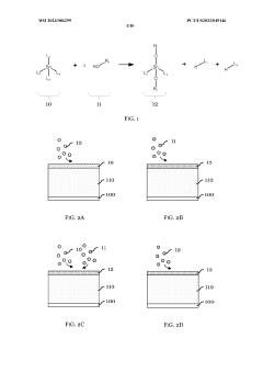
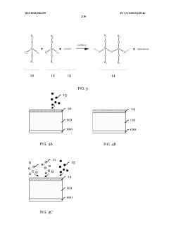
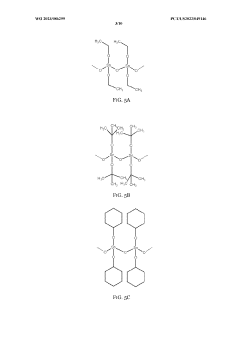
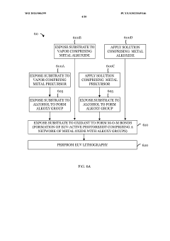
EUV active films for EUV lithography
PatentWO2023086299A1
Innovation
- A method of forming an EUV-active photoresist layer comprising a network of metal oxide terminated with alkoxy groups, specifically using a metal alkoxide moiety that responds to EUV exposure, enabling higher absorbance and improved etch resistance, and allowing for dry or wet development processes to achieve better control at the nanoscale.
Environmental Impact of EUV Photoresist Materials
The environmental impact of EUV photoresist materials represents a critical consideration in semiconductor manufacturing processes. These specialized polymers, designed to achieve nanometer-scale resolution under extreme ultraviolet exposure, contain various chemical compounds that pose potential environmental concerns throughout their lifecycle. The manufacturing, use, and disposal of these materials involve complex environmental trade-offs that must be carefully evaluated.
Primary environmental concerns stem from the chemical composition of EUV photoresists, which often contain metal-based compounds, fluorinated polymers, and photoacid generators. These components can persist in the environment and may bioaccumulate in ecosystems if improperly managed. The metal components, particularly tin and antimony used in some formulations to enhance sensitivity to EUV radiation, present specific toxicity concerns when released into aquatic environments.
Manufacturing processes for EUV photoresists consume significant energy and resources, contributing to their overall environmental footprint. The production of high-purity chemicals required for these advanced materials involves energy-intensive purification steps and generates waste streams containing solvents and unreacted precursors. Additionally, the specialized handling requirements for these materials necessitate controlled environments that further increase energy consumption.
During semiconductor fabrication, the application and development of photoresists generate substantial volumes of chemical waste. The development process typically uses organic solvents that must be captured and treated before disposal. While modern fabrication facilities implement advanced waste treatment systems, the complete elimination of environmental impacts remains challenging, particularly as production volumes increase to meet growing semiconductor demand.
End-of-life considerations for semiconductor products containing residual photoresist materials present additional environmental challenges. The complex nature of these products often complicates recycling efforts, potentially leading to landfill disposal where hazardous components may leach into soil and groundwater. Industry initiatives to develop more environmentally benign photoresist formulations have shown promise but face technical hurdles in maintaining the required performance characteristics.
Regulatory frameworks governing these materials continue to evolve globally, with increasing emphasis on reducing persistent, bioaccumulative, and toxic substances. Manufacturers must navigate complex compliance requirements while balancing performance demands. Recent research has focused on developing "greener" alternatives, including bio-based polymers and water-developable resists that could significantly reduce environmental impacts while maintaining the thermal stability necessary for EUV lithography processes.
Integration Challenges with Advanced Node Processes
The integration of EUV lithography into advanced node processes presents significant challenges, particularly concerning the thermal stability of photoresist polymers. As process nodes shrink below 7nm, the thermal budget constraints become increasingly stringent, creating a complex interplay between EUV exposure parameters and resist performance.
Advanced node integration requires precise control of thermal profiles during both pre-exposure and post-exposure bake processes. The chemical amplification mechanisms in EUV resists are highly temperature-sensitive, with even minor thermal fluctuations potentially causing critical dimension variations across the wafer. This thermal sensitivity becomes more pronounced as feature sizes approach sub-10nm dimensions.
The interaction between EUV photons (13.5nm wavelength) and resist polymers generates secondary electrons with varying energies, creating localized heating effects that can exceed 100°C in nanoscale regions. These transient thermal spikes may induce premature acid diffusion or polymer degradation, compromising pattern fidelity. Advanced node processes must therefore incorporate sophisticated thermal management strategies to mitigate these effects.
Material compatibility issues further complicate integration efforts. The underlayers and hard masks used in advanced node stacks must maintain thermal stability during resist processing while preserving their functional properties. Thermal expansion coefficient mismatches between these materials can induce mechanical stress, leading to pattern distortion or delamination during subsequent processing steps.
Defectivity control represents another critical integration challenge. Thermally-induced resist degradation can generate particles and residues that contaminate process equipment and reduce yield. Advanced metrology techniques, including in-line thermal imaging and real-time temperature monitoring, are becoming essential components of defect reduction strategies in EUV-based processes.
The narrow process window characteristic of advanced nodes leaves minimal margin for thermal variations. Engineers must balance competing requirements: sufficient thermal energy to activate chemical amplification mechanisms without triggering polymer decomposition or pattern collapse. This delicate balance necessitates precise temperature control systems with uniformity specifications often below ±0.1°C across 300mm wafers.
From a manufacturing perspective, the integration of thermally stable EUV resists requires holistic optimization across the entire process flow. Thermal history effects from preceding process steps (deposition, etch, implant) can significantly impact resist performance, necessitating comprehensive thermal budget management throughout the fabrication sequence.
Unlock deeper insights with Patsnap Eureka Quick Research — get a full tech report to explore trends and direct your research. Try now!
Generate Your Research Report Instantly with AI Agent
Supercharge your innovation with Patsnap Eureka AI Agent Platform!