Cross-Linking Kinetics in Chemically Amplified EUV Resists
OCT 13, 20259 MIN READ
Generate Your Research Report Instantly with AI Agent
Patsnap Eureka helps you evaluate technical feasibility & market potential.
EUV Resist Cross-Linking Background and Objectives
Extreme Ultraviolet (EUV) lithography represents a revolutionary advancement in semiconductor manufacturing, enabling the production of increasingly miniaturized integrated circuits with feature sizes below 7nm. At the heart of this technology lies the chemically amplified resist (CAR) systems, which have evolved significantly since their introduction in the 1980s to meet the demanding requirements of EUV lithography.
The cross-linking mechanism in EUV resists fundamentally differs from traditional deep ultraviolet (DUV) systems due to the significantly higher photon energy (13.5nm wavelength, approximately 92eV). This energy difference creates unique reaction pathways, generating secondary electrons that play a crucial role in the resist chemistry. Understanding these cross-linking kinetics has become essential for optimizing resist performance as the industry pushes toward smaller feature sizes.
Historically, resist technology has progressed from G-line (436nm) to I-line (365nm), then to KrF (248nm) and ArF (193nm) excimer laser systems, with each transition requiring significant chemical innovations. The leap to EUV represents the most challenging transition yet, demanding fundamental reconsideration of resist chemistry principles that have served the industry for decades.
The primary objective of investigating cross-linking kinetics in chemically amplified EUV resists is to enhance resolution capabilities while maintaining acceptable sensitivity and line edge roughness—the three key performance metrics often referred to as the "triangle trade-off" in resist technology. Current EUV resists struggle to simultaneously optimize these parameters, creating a significant technological bottleneck for next-generation semiconductor manufacturing.
Additional objectives include understanding the fundamental reaction mechanisms triggered by EUV photons, quantifying the contribution of secondary electrons to cross-linking efficiency, and developing predictive models that can accelerate resist formulation. These insights are crucial for designing resist systems that can support high-volume manufacturing at increasingly smaller technology nodes.
The technological evolution of EUV resists is further complicated by the need for compatibility with existing semiconductor manufacturing infrastructure, including development processes and etching techniques. This necessitates a comprehensive approach to resist design that considers not only the photochemical performance but also integration with the broader manufacturing ecosystem.
Recent advancements in analytical techniques, including femtosecond spectroscopy and synchrotron-based analysis methods, have enabled unprecedented insights into the ultrafast reactions occurring during EUV exposure. These tools provide the foundation for developing a more complete understanding of cross-linking kinetics and ultimately designing more effective resist systems for future technology nodes.
Market Analysis for Advanced Lithography Materials
The global market for advanced lithography materials, particularly those used in Extreme Ultraviolet (EUV) lithography, has experienced significant growth in recent years, driven by the semiconductor industry's push toward smaller node sizes. The EUV resist materials market, valued at approximately $380 million in 2022, is projected to reach $650 million by 2027, representing a compound annual growth rate of 11.3%. This growth is primarily fueled by the increasing adoption of EUV lithography in high-volume manufacturing by leading semiconductor companies.
Chemically Amplified (CA) EUV resists represent a substantial segment within this market, accounting for nearly 60% of the total EUV resist consumption. The demand for these materials is particularly strong in regions with concentrated semiconductor manufacturing capabilities, with East Asia (Taiwan, South Korea, and Japan) consuming approximately 70% of the global supply, followed by North America at 18% and Europe at 12%.
The market landscape is characterized by a high barrier to entry due to the complex chemistry and precision required in formulating EUV resists with optimal cross-linking kinetics. Currently, the market is dominated by specialized chemical suppliers including JSR Corporation, Tokyo Ohka Kogyo (TOK), Shin-Etsu Chemical, and DuPont, who collectively hold over 75% of the market share.
End-user industries driving demand include logic chip manufacturers (35%), memory producers (30%), and foundries (25%), with the remaining 10% distributed among various specialty semiconductor applications. The push toward 3nm and 2nm process nodes has intensified the demand for high-performance EUV resists with enhanced cross-linking properties.
Market analysis indicates that pricing premiums exist for EUV resists that demonstrate superior resolution capabilities, lower line edge roughness, and faster cross-linking kinetics. Materials that can achieve sub-10nm feature sizes while maintaining high sensitivity command price premiums of 30-40% compared to standard offerings.
Recent market trends show increasing customer preference for resist materials that balance sensitivity and resolution, with particular emphasis on reducing pattern collapse issues at smaller nodes. Additionally, there is growing demand for resists with improved environmental stability and reduced outgassing characteristics, driven by both manufacturing yield concerns and regulatory pressures.
The forecast for chemically amplified EUV resists remains strong, though emerging non-chemically amplified alternatives are gaining traction in specific applications. Market analysts predict that innovations in cross-linking mechanisms that address current sensitivity-resolution trade-offs could potentially capture significant market share within the next three to five years.
Current Challenges in EUV Resist Technology
Extreme Ultraviolet (EUV) lithography represents a significant advancement in semiconductor manufacturing, enabling the production of increasingly smaller and more complex integrated circuits. However, the resist technology for EUV lithography faces numerous challenges that impede its widespread adoption and optimal performance. The primary issue lies in the fundamental physics of EUV exposure, which operates at a wavelength of 13.5 nm and generates high-energy photons (91.6 eV) that interact with resist materials differently than traditional deep ultraviolet (DUV) light.
One of the most significant challenges is the low photon absorption efficiency in current resist materials. Unlike DUV lithography, where a single photon typically generates one chemical reaction, EUV requires multiple photons to initiate sufficient chemical changes. This low quantum yield necessitates higher exposure doses, reducing throughput and increasing production costs. Additionally, the stochastic effects become more pronounced at the nanoscale dimensions targeted by EUV lithography, leading to line edge roughness (LER) and pattern collapse issues.
The cross-linking kinetics in chemically amplified EUV resists present particular difficulties. These resists rely on acid-catalyzed reactions triggered by EUV radiation, but the acid diffusion mechanisms that work well for DUV resists often cause resolution limitations in EUV applications. The balance between sensitivity and resolution becomes increasingly difficult to maintain as feature sizes decrease below 20 nm. Furthermore, the secondary electron generation during EUV exposure complicates the reaction pathways and can lead to unintended cross-linking outside the targeted exposure areas.
Material compatibility issues also plague current EUV resist technology. Many promising resist formulations contain metal elements to enhance EUV absorption, but these can introduce contamination concerns in semiconductor fabrication environments. The integration of these novel materials into existing manufacturing processes requires extensive validation and often necessitates modifications to established workflows.
Outgassing during EUV exposure represents another critical challenge. The high-energy EUV photons can break chemical bonds in the resist, releasing volatile compounds that may contaminate the expensive EUV optics. This necessitates the development of resist materials with minimal outgassing properties while maintaining high sensitivity and resolution.
The limited understanding of reaction mechanisms at the molecular level further complicates resist development. The complex interplay between photon absorption, electron generation, acid production, and subsequent cross-linking reactions is not fully characterized, making rational design of improved resist systems challenging. Computational modeling approaches are still evolving to accurately predict resist performance under EUV exposure conditions.
State-of-the-Art Cross-Linking Mechanisms
01 Cross-linking mechanisms in EUV resist formulations
Chemically amplified EUV resists utilize specific cross-linking mechanisms to achieve high resolution patterns. These mechanisms involve photoacid generators that catalyze cross-linking reactions upon exposure to EUV radiation. The kinetics of these reactions are critical for controlling pattern formation, with factors such as acid diffusion length and reaction rate constants playing key roles in determining resolution and sensitivity. Advanced cross-linking agents are incorporated to enhance the efficiency of these reactions while maintaining pattern fidelity.- Cross-linking mechanisms in EUV resist formulations: Chemically amplified EUV resists utilize specific cross-linking mechanisms to achieve high resolution patterns. These mechanisms involve acid-catalyzed reactions that form covalent bonds between polymer chains upon exposure to EUV radiation. The cross-linking kinetics are influenced by the chemical structure of the polymer, the type and concentration of the photoacid generator, and the post-exposure bake conditions. Understanding these mechanisms is crucial for developing resists with improved sensitivity and pattern fidelity.
- Optimization of EUV resist sensitivity and resolution: The sensitivity and resolution of chemically amplified EUV resists can be optimized by controlling the cross-linking kinetics. This involves adjusting the concentration of photoacid generators, incorporating quenchers to control acid diffusion, and modifying the polymer backbone structure. The balance between sensitivity and resolution is critical, as higher sensitivity often comes at the cost of reduced resolution. Advanced formulations aim to achieve both high sensitivity to EUV radiation and excellent pattern resolution through precise control of the cross-linking process.
- Impact of post-exposure bake on cross-linking kinetics: Post-exposure bake (PEB) conditions significantly influence the cross-linking kinetics in chemically amplified EUV resists. The temperature and duration of the PEB affect the diffusion of the photogenerated acid and the rate of the cross-linking reactions. Optimizing these parameters is essential for controlling line edge roughness, pattern collapse, and overall resist performance. Advanced PEB protocols may involve temperature gradients or multi-step processes to fine-tune the cross-linking behavior for specific applications.
- Novel materials for enhanced EUV resist performance: Research into novel materials for EUV resists focuses on developing polymers and additives that can improve cross-linking kinetics. Metal-containing resists, nanoparticle-based systems, and hybrid organic-inorganic materials are being explored to enhance EUV absorption and catalytic efficiency. These materials aim to address the challenges of traditional chemically amplified resists, such as pattern collapse at small feature sizes and limited sensitivity to EUV radiation. The incorporation of these novel materials can significantly alter the cross-linking mechanisms and kinetics.
- Analytical techniques for studying cross-linking kinetics: Various analytical techniques are employed to study and characterize the cross-linking kinetics in EUV resists. These include real-time Fourier transform infrared spectroscopy (FTIR), quartz crystal microbalance (QCM) measurements, atomic force microscopy (AFM), and specialized lithographic evaluation tools. These techniques provide insights into the reaction rates, diffusion processes, and structural changes occurring during exposure and post-exposure bake. The data obtained from these analyses help in developing mathematical models that can predict resist performance and guide formulation optimization.
02 Optimization of acid diffusion in EUV resist systems
The control of acid diffusion is crucial for achieving high resolution in chemically amplified EUV resists. The kinetics of acid diffusion significantly impact cross-linking reactions and pattern formation. Various approaches are employed to optimize acid diffusion, including the use of quenchers, base additives, and polymer matrix modifications. These strategies help to control the diffusion length of photogenerated acids, thereby improving resolution, line edge roughness, and overall pattern quality in EUV lithography processes.Expand Specific Solutions03 Temperature effects on cross-linking kinetics
Temperature plays a critical role in the cross-linking kinetics of chemically amplified EUV resists. Post-exposure bake (PEB) conditions significantly influence reaction rates, acid diffusion, and ultimately pattern formation. The activation energy of cross-linking reactions determines temperature sensitivity, which must be carefully controlled to achieve optimal performance. Advanced thermal processing techniques are developed to manage the temperature-dependent kinetics, enabling precise control over cross-linking reactions and improving resist performance metrics such as sensitivity and resolution.Expand Specific Solutions04 Novel polymer architectures for enhanced cross-linking
Innovative polymer designs are being developed to enhance cross-linking efficiency in EUV resist systems. These include polymers with specialized functional groups that facilitate rapid and controlled cross-linking upon acid generation. The architecture of these polymers influences the kinetics of cross-linking reactions, with factors such as molecular weight, polydispersity, and functional group density playing important roles. Advanced polymer designs incorporate features that balance cross-linking efficiency with other critical properties such as etch resistance and pattern collapse resistance.Expand Specific Solutions05 Measurement and modeling of cross-linking kinetics
Advanced analytical techniques are employed to measure and model the cross-linking kinetics in chemically amplified EUV resists. These include real-time monitoring methods such as FTIR spectroscopy, quartz crystal microbalance, and specialized optical techniques that track the progression of cross-linking reactions. Computational modeling approaches are also developed to simulate the complex interplay between acid diffusion, cross-linking reactions, and pattern formation. These measurement and modeling tools enable the optimization of resist formulations and processing conditions to achieve desired performance characteristics.Expand Specific Solutions
Leading Companies in EUV Resist Development
The cross-linking kinetics in chemically amplified EUV resists market is currently in a growth phase, with increasing demand driven by semiconductor manufacturing advancements. The market is expected to expand significantly as EUV lithography adoption accelerates, particularly with major players like TSMC and Infineon Technologies investing heavily in this technology. Leading companies including TOKYO OHKA KOGYO, Sumitomo Chemical, and FUJIFILM are at the forefront of resist technology development, with varying degrees of technical maturity. Research institutions like Tsinghua University and CNRS are contributing fundamental innovations, while specialized firms such as Irresistible Materials are developing next-generation materials. The competitive landscape features established chemical giants like BASF alongside specialized resist manufacturers, creating a dynamic ecosystem of innovation focused on improving resolution, sensitivity, and line edge roughness performance.
Taiwan Semiconductor Manufacturing Co., Ltd.
Technical Solution: TSMC has developed a comprehensive approach to EUV resist integration focusing on optimizing cross-linking kinetics for high-volume manufacturing environments. Their technology combines materials engineering with advanced process control to achieve reliable patterning at 5nm and below. TSMC's approach includes customized resist formulations co-developed with material suppliers, featuring tailored acid diffusion characteristics and optimized protecting group chemistry. The company has implemented sophisticated post-exposure bake (PEB) protocols that precisely control temperature profiles to manage cross-linking reactions, resulting in improved critical dimension uniformity across wafers. TSMC has also pioneered the integration of metal-containing hybrid resists that enhance EUV absorption efficiency while maintaining compatibility with their process flows. Their research has demonstrated that carefully controlled cross-linking kinetics significantly impacts pattern collapse behavior, leading to the development of specialized rinse chemistries and drying techniques that preserve fine features after development. TSMC's holistic approach extends to customized track systems with precise temperature control that ensures consistent cross-linking behavior across high-volume production.
Strengths: Proven integration capability in high-volume manufacturing environments, comprehensive process control systems that ensure consistent performance, and demonstrated success at leading-edge technology nodes. Weaknesses: Heavy dependence on specialized equipment configurations, potentially higher overall process costs, and challenges in transferring optimized processes across different manufacturing sites.
TOKYO OHKA KOGYO CO., LTD.
Technical Solution: Tokyo Ohka Kogyo (TOK) has developed advanced EUV resist materials with optimized cross-linking kinetics through their proprietary molecular design approach. Their technology focuses on controlling acid diffusion in chemically amplified resists (CARs) through the incorporation of specialized quencher molecules and acid generators. TOK's EUV resist formulations feature precisely engineered polymer backbones with tailored protecting groups that undergo controlled deprotection during post-exposure baking. The company has achieved significant improvements in resolution capabilities, reaching sub-10nm feature sizes with reduced line edge roughness (LER). Their latest generation of EUV resists incorporates metal-oxide nanoparticles to enhance sensitivity while maintaining high resolution. TOK has also developed specialized post-exposure bake (PEB) processes that optimize the cross-linking reaction kinetics, resulting in improved pattern fidelity and reduced defectivity rates compared to conventional approaches.
Strengths: Superior resolution capability with demonstrated sub-10nm patterning, excellent integration with existing semiconductor manufacturing processes, and balanced sensitivity-resolution-LER performance. Weaknesses: Higher material costs compared to traditional resists, potential for metal contamination in metal-oxide containing formulations, and relatively narrow process windows requiring precise control of exposure and PEB conditions.
Key Patents in EUV Resist Cross-Linking Technology
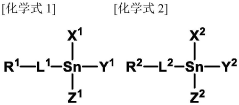
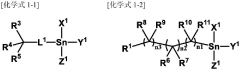
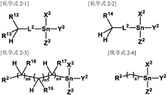
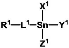
Semiconductor photoresist composition and method of forming pattern using the same
PatentPendingCN117492324A
Innovation
- Using a semiconductor photoresist composition composed of a specific organic metal compound, including a first organic metal compound and a second organic metal compound, by improving the sensitivity and storage stability of the photoresist, combined with a surfactant, a cross-linking agent, etc. Additives to form high performance photoresists.
EUV metallic resist performance enhancement via additives
PatentPendingUS20240377735A1
Innovation
- Incorporating additives such as high boiling point solvents, photo acid generators, photo base generators, quenchers, photo decomposed bases, thermal acid generators, and photo sensitivity cross-linkers into the metallic photoresist materials to enhance their shelf life and CD control, specifically targeting the instability and variability issues in metallic resists.
Environmental Impact of EUV Resist Materials
The environmental impact of EUV resist materials represents a critical consideration in the semiconductor industry's sustainability efforts. Chemically amplified EUV resists, while enabling cutting-edge lithography processes, contain compounds that pose significant environmental concerns throughout their lifecycle. These materials typically incorporate photoacid generators (PAGs), quenchers, and polymer matrices containing fluorinated compounds, which can persist in the environment and potentially bioaccumulate.
During manufacturing processes, the production of EUV resist materials requires hazardous chemicals including strong acids, organic solvents, and metal-containing compounds. The synthesis of these specialized polymers and additives generates substantial waste streams that require careful treatment and disposal. Estimates suggest that for each kilogram of resist produced, approximately 5-10 kilograms of chemical waste may be generated.
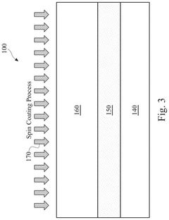
In semiconductor fabrication facilities, EUV resist application involves volatile organic compounds (VOCs) that contribute to air pollution and potential worker exposure. The spin-coating process typically wastes 95-98% of the applied resist material, creating significant disposal challenges. Additionally, the development and stripping processes utilize alkaline solutions and organic solvents that enter wastewater streams, requiring extensive treatment before release.
End-of-life considerations for semiconductor devices containing residual resist materials present further environmental challenges. The cross-linked nature of exposed resists makes them particularly resistant to environmental degradation, potentially persisting for decades. Studies have detected fluorinated compounds from semiconductor manufacturing in groundwater near production facilities, raising concerns about long-term environmental impacts.
Recent regulatory developments, including the European Union's REACH regulations and similar frameworks in Asia and North America, have begun restricting certain chemicals commonly used in resist formulations. This regulatory landscape is driving research into "greener" EUV resist alternatives that maintain performance while reducing environmental footprint. Several approaches show promise, including bio-based polymers, metal-oxide resists with reduced toxicity, and processes designed to minimize waste generation.
Industry initiatives like the Semiconductor Environmental Safety and Health Association (SESHA) have established guidelines for responsible management of resist materials. Leading semiconductor manufacturers have implemented closed-loop recycling systems for solvents and developers, significantly reducing waste volumes. Advanced treatment technologies, including supercritical CO2 cleaning and plasma-based processes, are being explored to minimize the environmental impact of resist processing steps.
During manufacturing processes, the production of EUV resist materials requires hazardous chemicals including strong acids, organic solvents, and metal-containing compounds. The synthesis of these specialized polymers and additives generates substantial waste streams that require careful treatment and disposal. Estimates suggest that for each kilogram of resist produced, approximately 5-10 kilograms of chemical waste may be generated.
In semiconductor fabrication facilities, EUV resist application involves volatile organic compounds (VOCs) that contribute to air pollution and potential worker exposure. The spin-coating process typically wastes 95-98% of the applied resist material, creating significant disposal challenges. Additionally, the development and stripping processes utilize alkaline solutions and organic solvents that enter wastewater streams, requiring extensive treatment before release.
End-of-life considerations for semiconductor devices containing residual resist materials present further environmental challenges. The cross-linked nature of exposed resists makes them particularly resistant to environmental degradation, potentially persisting for decades. Studies have detected fluorinated compounds from semiconductor manufacturing in groundwater near production facilities, raising concerns about long-term environmental impacts.
Recent regulatory developments, including the European Union's REACH regulations and similar frameworks in Asia and North America, have begun restricting certain chemicals commonly used in resist formulations. This regulatory landscape is driving research into "greener" EUV resist alternatives that maintain performance while reducing environmental footprint. Several approaches show promise, including bio-based polymers, metal-oxide resists with reduced toxicity, and processes designed to minimize waste generation.
Industry initiatives like the Semiconductor Environmental Safety and Health Association (SESHA) have established guidelines for responsible management of resist materials. Leading semiconductor manufacturers have implemented closed-loop recycling systems for solvents and developers, significantly reducing waste volumes. Advanced treatment technologies, including supercritical CO2 cleaning and plasma-based processes, are being explored to minimize the environmental impact of resist processing steps.
Integration with Semiconductor Manufacturing Processes
The integration of Chemically Amplified EUV Resists into semiconductor manufacturing processes represents a critical junction where theoretical research meets industrial application. Current semiconductor fabrication facilities must adapt their process flows to accommodate the unique cross-linking kinetics exhibited by these advanced resist materials. This adaptation requires careful consideration of thermal processing parameters, as the post-exposure bake (PEB) step significantly influences the acid diffusion and subsequent cross-linking reactions in EUV resists.
Manufacturing integration challenges primarily stem from the sensitivity of cross-linking kinetics to environmental conditions. Fabrication facilities must maintain exceptionally tight control over humidity, temperature, and airborne molecular contaminants (AMCs) to ensure consistent resist performance. Even minor variations in these parameters can dramatically alter acid diffusion rates, leading to inconsistent feature dimensions and reduced yield. Advanced environmental control systems with parts-per-billion precision have become essential infrastructure components for facilities utilizing chemically amplified EUV resists.
Process compatibility issues also emerge when integrating these resists into established manufacturing flows. The interaction between EUV resists and underlying anti-reflective coatings, hard masks, or previously deposited materials can influence cross-linking behavior at interfaces. This necessitates comprehensive material compatibility testing and often requires the development of specialized interface layers to maintain resist performance while preserving the integrity of underlying structures.
Metrology and inspection systems require significant recalibration when working with EUV resists due to their unique optical properties and cross-linking mechanisms. Traditional optical inspection tools may struggle to accurately measure partially cross-linked structures, necessitating the development of specialized metrology approaches. Advanced techniques such as scatterometry and critical dimension small-angle X-ray scatterometry (CD-SAXS) are increasingly being deployed to characterize these materials within production environments.
Equipment manufacturers have responded by developing specialized tools designed specifically for EUV resist processing. These include precision coating systems capable of achieving nanometer-level thickness uniformity, advanced PEB stations with sub-degree temperature control across 300mm wafers, and development systems optimized for the unique dissolution characteristics of cross-linked EUV resists. The capital investment required for these specialized tools represents a significant barrier to entry for semiconductor manufacturers considering EUV lithography adoption.
Time-to-market pressures further complicate integration efforts, as manufacturers must balance process optimization with production schedules. The complex interplay between resist chemistry, process conditions, and equipment parameters necessitates extensive characterization and qualification cycles. Leading semiconductor manufacturers have established dedicated process integration teams focused specifically on optimizing EUV resist performance within their unique manufacturing environments.
Unlock deeper insights with Patsnap Eureka Quick Research — get a full tech report to explore trends and direct your research. Try now!
Generate Your Research Report Instantly with AI Agent
Supercharge your innovation with Patsnap Eureka AI Agent Platform!