

Resist–Substrate Interface Adhesion Mechanisms
OCT 13, 20259 MIN READ
Generate Your Research Report Instantly with AI Agent
Patsnap Eureka helps you evaluate technical feasibility & market potential.
Resist-Substrate Adhesion Background and Objectives
Photoresist adhesion to substrates represents a fundamental aspect of semiconductor manufacturing, with its origins dating back to the early development of integrated circuits in the 1960s. The evolution of this technology has been driven by the continuous miniaturization of electronic components, following Moore's Law, which has pushed the boundaries of photolithography processes. Initially, adhesion mechanisms relied on simple physical interactions, but as feature sizes decreased below the micron scale, more sophisticated approaches became necessary to maintain pattern integrity.
The adhesion between photoresist and substrate materials involves complex physicochemical interactions that determine the success of subsequent processing steps. These interactions include van der Waals forces, hydrogen bonding, chemical bonding, and electrostatic forces, all of which contribute to the overall adhesion strength. Understanding these mechanisms has become increasingly critical as the semiconductor industry progresses toward sub-10nm nodes, where even minor adhesion failures can lead to catastrophic yield losses.
Recent technological advancements have introduced new materials and processes that present unique adhesion challenges. High-k dielectrics, III-V semiconductors, and various metal substrates each require tailored adhesion promotion strategies. Additionally, the introduction of extreme ultraviolet (EUV) lithography has further complicated adhesion requirements due to the higher energy radiation and thinner resist films involved.
The primary objective of this research is to develop a comprehensive understanding of the fundamental mechanisms governing resist-substrate adhesion across various material systems. This includes identifying the key parameters that influence adhesion strength, such as surface energy, roughness, chemical functionality, and environmental conditions. By elucidating these mechanisms, we aim to establish predictive models that can guide the development of next-generation adhesion promotion techniques.
Furthermore, this research seeks to address critical challenges in emerging applications, including flexible electronics, 3D integration, and nanoimprint lithography, where traditional adhesion approaches may prove inadequate. The goal is to develop universal principles that can be applied across diverse technological platforms while accommodating specific material requirements.
Another important objective is to investigate environmentally friendly alternatives to conventional adhesion promoters, many of which contain hazardous chemicals like hexamethyldisilazane (HMDS). As sustainability becomes increasingly important in semiconductor manufacturing, developing green adhesion promotion technologies represents a significant research direction with both environmental and economic benefits.
Market Analysis for Adhesion Enhancement Solutions
The global market for adhesion enhancement solutions in semiconductor manufacturing is experiencing robust growth, driven primarily by the increasing complexity of semiconductor devices and the continuous miniaturization of feature sizes. As of 2023, the market for specialty chemicals used in semiconductor adhesion applications is valued at approximately $3.2 billion, with a projected compound annual growth rate of 6.8% through 2028.
The demand for advanced adhesion promoters is particularly strong in regions with high semiconductor manufacturing activity, including East Asia (Taiwan, South Korea, Japan), North America, and Western Europe. Taiwan and South Korea together account for over 40% of the global market consumption, reflecting their dominance in advanced semiconductor fabrication.
Market segmentation reveals distinct categories within the adhesion enhancement solutions landscape. Traditional hexamethyldisilazane (HMDS) primers continue to hold the largest market share at 45%, though this percentage is gradually declining. Newer silane-based adhesion promoters are gaining traction, currently representing 30% of the market with the highest growth rate among all segments. Specialized polymer-based solutions and novel vapor-phase treatments constitute the remaining market share.
End-user analysis indicates that integrated device manufacturers (IDMs) and foundries are the primary consumers, accounting for 78% of total market demand. Research institutions and specialty semiconductor manufacturers make up the remainder, often serving as early adopters for innovative adhesion technologies.
The market is experiencing several notable trends that will shape its future trajectory. First, there is increasing demand for adhesion solutions compatible with extreme ultraviolet (EUV) lithography processes, as this technology becomes more prevalent in advanced node manufacturing. Second, environmentally friendly adhesion promoters with reduced volatile organic compound (VOC) content are gaining market share due to stricter regulatory requirements in major manufacturing regions.
Key market drivers include the growing adoption of 3D integration technologies, which create new interfaces requiring robust adhesion solutions, and the expansion of semiconductor applications in emerging fields such as quantum computing and bioelectronics. Additionally, the trend toward more complex multi-layer resist systems is creating demand for specialized interface engineering solutions.
Market challenges primarily revolve around cost pressures from semiconductor manufacturers seeking to optimize production expenses while maintaining performance, and the technical difficulties in developing adhesion solutions that work effectively across increasingly diverse material combinations used in advanced semiconductor devices.
Current Adhesion Mechanisms and Technical Barriers
The adhesion between photoresist and substrate surfaces represents a critical factor in semiconductor manufacturing processes. Currently, several mechanisms contribute to this interfacial adhesion. Chemical bonding serves as the primary mechanism, where covalent or hydrogen bonds form between functional groups in the resist and reactive sites on the substrate surface. Van der Waals forces and electrostatic interactions provide secondary adhesion mechanisms, particularly important when chemical bonding opportunities are limited.
Surface preparation techniques significantly influence adhesion quality. Industry standard approaches include vapor priming with hexamethyldisilazane (HMDS), which creates a hydrophobic surface through silylation reactions with hydroxyl groups on the substrate. This process effectively reduces water adsorption that would otherwise interfere with adhesion. Plasma treatment represents another widely adopted method, where oxygen or argon plasma activates the substrate surface by creating reactive sites and removing organic contaminants.
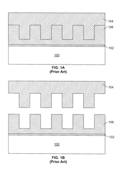
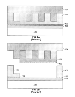
Despite these established mechanisms and techniques, several technical barriers persist in achieving optimal adhesion. Pattern collapse during development represents a major challenge, particularly as feature sizes continue to shrink below 10nm. The increasing aspect ratios of these features create capillary forces during the drying process that can overcome adhesion strength. This issue becomes more pronounced with EUV lithography implementation.
Material compatibility issues present another significant barrier. Advanced node processes often require complex substrate stacks with various materials (silicon, silicon dioxide, silicon nitride, metals, etc.), each exhibiting different surface energies and chemical properties. Developing universal adhesion promoters that work effectively across these diverse surfaces remains challenging.
Environmental sensitivity constitutes a persistent obstacle, as humidity and temperature fluctuations during processing can dramatically impact adhesion quality. Even minor variations in these parameters can lead to inconsistent results, particularly in high-volume manufacturing environments where tight process control is essential.
The increasing complexity of resist formulations introduces additional challenges. As resists incorporate more components to meet performance requirements (sensitivity enhancers, quenchers, etc.), their interaction with substrate surfaces becomes more unpredictable, requiring more sophisticated adhesion promotion strategies.
Finally, metrology limitations hinder progress in this field. Current techniques for quantifying adhesion strength at the nanoscale lack precision and reproducibility, making it difficult to systematically optimize adhesion mechanisms or compare different approaches objectively.
Surface preparation techniques significantly influence adhesion quality. Industry standard approaches include vapor priming with hexamethyldisilazane (HMDS), which creates a hydrophobic surface through silylation reactions with hydroxyl groups on the substrate. This process effectively reduces water adsorption that would otherwise interfere with adhesion. Plasma treatment represents another widely adopted method, where oxygen or argon plasma activates the substrate surface by creating reactive sites and removing organic contaminants.
Despite these established mechanisms and techniques, several technical barriers persist in achieving optimal adhesion. Pattern collapse during development represents a major challenge, particularly as feature sizes continue to shrink below 10nm. The increasing aspect ratios of these features create capillary forces during the drying process that can overcome adhesion strength. This issue becomes more pronounced with EUV lithography implementation.
Material compatibility issues present another significant barrier. Advanced node processes often require complex substrate stacks with various materials (silicon, silicon dioxide, silicon nitride, metals, etc.), each exhibiting different surface energies and chemical properties. Developing universal adhesion promoters that work effectively across these diverse surfaces remains challenging.
Environmental sensitivity constitutes a persistent obstacle, as humidity and temperature fluctuations during processing can dramatically impact adhesion quality. Even minor variations in these parameters can lead to inconsistent results, particularly in high-volume manufacturing environments where tight process control is essential.
The increasing complexity of resist formulations introduces additional challenges. As resists incorporate more components to meet performance requirements (sensitivity enhancers, quenchers, etc.), their interaction with substrate surfaces becomes more unpredictable, requiring more sophisticated adhesion promotion strategies.
Finally, metrology limitations hinder progress in this field. Current techniques for quantifying adhesion strength at the nanoscale lack precision and reproducibility, making it difficult to systematically optimize adhesion mechanisms or compare different approaches objectively.
Contemporary Adhesion Enhancement Methodologies
01 Adhesion promoters for resist-substrate interface
Adhesion promoters are used to enhance the bonding between photoresist materials and substrate surfaces. These compounds, such as hexamethyldisilazane (HMDS) and other silane coupling agents, create chemical bonds between the resist and substrate, significantly improving adhesion. The promoters are typically applied as a thin layer before the resist coating process, forming a molecular bridge that increases interface stability and prevents resist lifting or delamination during development and etching processes.- Adhesion promoters for resist-substrate interface: Adhesion promoters are compounds that enhance the bonding between photoresist and substrate surfaces. These materials typically contain functional groups that can form chemical bonds with both the substrate (often silicon-based) and the resist material. Common adhesion promoters include silanes, titanates, and other coupling agents that create a molecular bridge between the different materials. The application of these promoters as a pre-treatment step significantly improves resist adhesion, reducing issues like delamination and pattern failure during subsequent processing steps.
- Surface treatment methods to enhance adhesion: Various surface treatment methods can be employed to improve the adhesion between resist and substrate. These include plasma treatment, UV-ozone cleaning, chemical etching, and thermal processing. Such treatments modify the surface energy, remove contaminants, create reactive sites, or alter the surface morphology of the substrate. These modifications promote stronger mechanical and chemical bonding with the subsequently applied resist layer, resulting in improved adhesion characteristics and more reliable pattern transfer during lithographic processes.
- Resist formulation for improved substrate adhesion: The composition of the resist material itself can be modified to enhance adhesion to various substrate materials. By incorporating specific functional groups, polymers, or additives into the resist formulation, the interfacial interactions with the substrate can be strengthened. These modifications may include adding polar groups to increase hydrogen bonding, incorporating cross-linking agents, or adjusting the molecular weight distribution of the polymers. Such formulation strategies improve adhesion without requiring additional processing steps or adhesion promoters.
- Multilayer resist systems for adhesion improvement: Multilayer resist systems utilize intermediate layers between the substrate and the imaging resist to enhance adhesion and improve overall lithographic performance. These systems may include bottom anti-reflective coatings (BARCs), underlayers, or specialized adhesion layers that are specifically designed to bond well with both the substrate and the imaging resist. The intermediate layers can be tailored to specific substrate materials and process conditions, providing enhanced adhesion while also offering additional benefits such as reflection control and planarization.
- Substrate surface modification techniques: Permanent or semi-permanent modifications to the substrate surface can significantly improve resist adhesion. These techniques include deposition of thin adhesion layers, surface roughening, chemical functionalization, or the creation of specific surface morphologies. Such modifications alter the physical and chemical properties of the substrate surface to create stronger bonds with resist materials. These approaches are particularly valuable for challenging substrates or when conventional adhesion promotion methods are insufficient for the required process conditions.
02 Surface treatment methods to enhance adhesion
Various surface treatment methods can be employed to improve resist-substrate adhesion. These include plasma treatment, UV-ozone cleaning, and chemical etching processes that modify the substrate surface properties. Such treatments remove contaminants, increase surface energy, create micro-roughness, or generate reactive sites on the substrate surface. These modifications promote stronger mechanical and chemical bonding with the resist layer, resulting in improved adhesion characteristics and reduced defects in subsequent processing steps.Expand Specific Solutions03 Resist formulation modifications for improved adhesion
Modifications to photoresist formulations can significantly enhance adhesion to various substrate materials. These modifications include incorporating adhesion-promoting functional groups, adjusting polymer molecular weight, and optimizing solvent systems. Additives such as cross-linking agents and reactive monomers can be included to create stronger bonds with the substrate surface. The balance of hydrophilic and hydrophobic components in the resist formulation also plays a crucial role in determining interface adhesion properties.Expand Specific Solutions04 Substrate material selection and preparation
The choice and preparation of substrate materials significantly impact resist adhesion. Different substrate materials (silicon, glass, metals, polymers) require specific preparation techniques to achieve optimal adhesion. Cleaning protocols to remove organic contaminants, native oxides, and moisture are essential. Surface roughness control, thermal treatments, and chemical conditioning of the substrate prior to resist application can dramatically improve interface adhesion and reduce defects in the patterning process.Expand Specific Solutions05 Process parameters affecting resist-substrate adhesion
Various process parameters significantly influence the adhesion between resist and substrate. These include coating conditions (spin speed, acceleration, temperature), baking parameters (temperature, time, ramp rate), humidity control during processing, and development conditions. Optimizing these parameters can enhance the wetting behavior of the resist on the substrate, promote solvent evaporation patterns that favor adhesion, and control stress at the interface. Advanced techniques such as vacuum contact during coating or specialized baking profiles can further improve adhesion in challenging applications.Expand Specific Solutions
Leading Organizations in Adhesion Research
The resist-substrate interface adhesion mechanisms research is currently in a growth phase, with increasing market demand driven by semiconductor miniaturization challenges. The technology maturity varies across key players, with established leaders like TSMC, IBM, and Tokyo Ohka Kogyo demonstrating advanced capabilities in photoresist adhesion technologies. Academic institutions including Carnegie Mellon University and Lanzhou Institute of Chemical Physics contribute fundamental research, while companies like Corning and RESONAC focus on specialized material solutions. The competitive landscape features collaboration between research institutions and industry manufacturers, with semiconductor giants like SMIC and BOE Technology integrating these adhesion technologies into their manufacturing processes to address critical yield and reliability challenges in next-generation semiconductor devices.
Taiwan Semiconductor Manufacturing Co., Ltd.
Technical Solution: TSMC has developed proprietary surface modification technologies for resist-substrate adhesion focusing on advanced node semiconductor manufacturing. Their approach combines chemical vapor deposition of specialized adhesion promoters with plasma treatment processes that create optimal surface energy conditions at the interface. TSMC's research includes multi-layer adhesion promotion systems where different molecular components address specific aspects of the adhesion mechanism, including mechanical interlocking, chemical bonding, and van der Waals interactions. They've implemented in-line metrology systems that quantitatively measure adhesion strength during production, enabling real-time process adjustments. TSMC has also pioneered temperature-controlled adhesion promotion processes that optimize molecular orientation at the interface, particularly important for high-aspect-ratio features in advanced nodes below 5nm.
Strengths: Highly optimized for advanced semiconductor manufacturing processes; integrated with production metrology; proven at scale in high-volume manufacturing. Weaknesses: Technologies likely specialized for silicon-based substrates; potentially less applicable to emerging substrate materials or non-semiconductor applications.
TOKYO OHKA KOGYO CO., LTD.
Technical Solution: TOK has developed specialized adhesion promotion systems focusing on chemical compatibility between resist formulations and various substrate materials. Their approach centers on tailored adhesion promoter molecules with specific functional groups designed to form strong chemical bonds with both the substrate and resist materials. TOK's research includes development of novel organosilicon compounds that provide superior adhesion performance compared to traditional HMDS, particularly for challenging substrate materials like silicon nitride and metal surfaces. They've created bottom anti-reflective coatings (BARCs) with dual functionality - reducing reflection while simultaneously enhancing adhesion through specialized interface chemistry. TOK has also pioneered water-soluble adhesion promoters that reduce environmental impact while maintaining performance comparable to solvent-based systems, addressing growing sustainability concerns in semiconductor manufacturing.
Strengths: Specialized expertise in resist chemistry and formulation; solutions tailored for specific substrate-resist combinations; strong focus on environmental sustainability. Weaknesses: May require integration with other process steps from different vendors; potentially less vertical integration compared to IDMs.
Critical Patents and Literature on Interface Mechanisms
Resist coated metal- or semiconductor-substrate having a stable resist-substrate adhesion
PatentInactiveEP0592972A3
Innovation
- A monomolecular layer of bifunctional organic molecules with selectively reactive functional groups is applied to the substrate, which reacts with the substrate surface to form a self-organizing monolayer, allowing for chemical bonding with the resist material during polymerization, ensuring strong adhesion without surface roughening and maintaining radiation sensitivity by localized adhesion promotion.
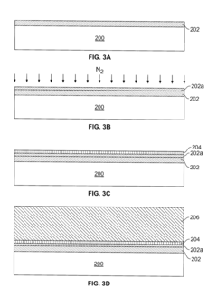
Resist adhension to carbon overcoats for nanoimprint lithography
PatentInactiveUS20110195276A1
Innovation
- Introducing nitrogen into the upper surface region of the COC layer to increase its surface energy and reactivity, allowing for covalent bonding with adhesion layers and improving resist adhesion.
Materials Compatibility and Surface Chemistry Considerations
The compatibility between resist materials and substrate surfaces plays a crucial role in determining adhesion strength at their interface. Different resist formulations exhibit varying degrees of compatibility with specific substrate materials, necessitating careful selection based on chemical composition and surface properties. For instance, novolac-based photoresists demonstrate excellent adhesion to silicon and silicon dioxide surfaces due to favorable hydrogen bonding interactions, while they may perform poorly on metallic surfaces without proper adhesion promoters.
Surface chemistry considerations are fundamental to understanding and optimizing resist-substrate adhesion. The presence of hydroxyl groups on silicon-based substrates facilitates strong chemical bonding with resist materials containing complementary functional groups. Conversely, hydrophobic surfaces often require specialized adhesion promotion techniques to achieve reliable resist adhesion. The surface energy mismatch between resist and substrate materials can significantly impact wetting behavior and subsequent adhesion quality, with optimal adhesion typically occurring when the surface energies are well-matched.
Chemical pretreatments significantly influence interface adhesion by modifying surface properties. Hexamethyldisilazane (HMDS) treatment, widely used in semiconductor manufacturing, replaces surface hydroxyl groups with trimethylsilyl groups, creating a hydrophobic surface that improves resist adhesion by reducing moisture interference. Similarly, oxygen plasma treatments increase surface energy and create reactive sites that enhance chemical bonding with resist materials.
Environmental factors, particularly humidity and temperature, dramatically affect surface chemistry at the resist-substrate interface. High humidity environments can lead to water molecule adsorption on substrate surfaces, forming a thin moisture layer that interferes with adhesion promoters and resist bonding. Temperature fluctuations during processing can alter surface energy characteristics and chemical reaction rates at the interface, potentially compromising adhesion integrity.
Metal substrates present unique compatibility challenges due to their distinct surface chemistry. Aluminum, copper, and titanium surfaces often develop native oxide layers with varying thicknesses and compositions, creating inconsistent adhesion profiles. These substrates frequently require specialized adhesion promoters containing metal-specific binding groups to achieve reliable resist adhesion. Additionally, the potential for galvanic interactions between certain metals and resist components necessitates careful material selection to prevent degradation of either component during processing.
Emerging substrate materials, including various polymers, ceramics, and compound semiconductors, introduce new compatibility considerations that require tailored approaches to surface chemistry modification. The development of universal adhesion promotion systems remains challenging due to the diverse chemical nature of these advanced materials, driving research toward more adaptable interface engineering solutions.
Environmental Impact of Adhesion Promotion Techniques
The environmental impact of adhesion promotion techniques in resist-substrate interfaces represents a critical consideration in modern semiconductor manufacturing processes. Traditional adhesion promoters, particularly those containing hexamethyldisilazane (HMDS), have raised significant environmental concerns due to their volatile organic compound (VOC) emissions. These compounds contribute to air pollution and pose potential health risks to workers in fabrication facilities. Studies have shown that HMDS vapor treatments can release substantial amounts of VOCs during processing, with measurements indicating concentrations that may exceed regulatory thresholds in some manufacturing environments.
Water consumption presents another environmental challenge, as many adhesion promotion processes require extensive rinsing and cleaning steps. The semiconductor industry's water footprint is already substantial, with estimates suggesting that producing a single 300mm wafer may require up to 2,000 gallons of ultra-pure water. Adhesion promotion techniques that minimize water usage therefore represent an important area for environmental improvement.
Chemical waste generation from adhesion promotion processes creates additional environmental burdens. The disposal of spent adhesion promoters, cleaning solutions, and associated materials often involves hazardous waste management protocols. This waste stream contains potentially harmful substances including silanes, organic solvents, and various metal contaminants that require specialized treatment before disposal.
Energy consumption constitutes a further environmental consideration. Thermal processing methods for adhesion promotion, such as dehydration baking and vapor priming, demand significant energy inputs. These processes typically operate at elevated temperatures (80-200°C) for extended periods, contributing to the overall carbon footprint of semiconductor manufacturing operations.
Recent regulatory developments have accelerated the transition toward more environmentally sustainable adhesion promotion techniques. The European Union's REACH regulations and similar frameworks in other regions have placed restrictions on certain chemicals commonly used in adhesion promotion, driving innovation toward greener alternatives. This regulatory landscape has catalyzed research into water-based adhesion promoters, solvent-free application methods, and plasma treatment technologies with reduced environmental impacts.
Life cycle assessment (LCA) studies comparing different adhesion promotion techniques have emerged as valuable tools for quantifying environmental impacts. These analyses typically evaluate factors including global warming potential, acidification potential, and resource depletion across the entire process chain. Recent LCA research indicates that plasma-based adhesion promotion may offer significant environmental advantages over traditional chemical methods when considering the complete environmental footprint.
Unlock deeper insights with Patsnap Eureka Quick Research — get a full tech report to explore trends and direct your research. Try now!
Generate Your Research Report Instantly with AI Agent
Supercharge your innovation with Patsnap Eureka AI Agent Platform!