Nanoparticle-Based EUV Resist Materials for Sub-5 nm Nodes
OCT 13, 20259 MIN READ
Generate Your Research Report Instantly with AI Agent
Patsnap Eureka helps you evaluate technical feasibility & market potential.
EUV Lithography Evolution and Objectives
Extreme Ultraviolet (EUV) lithography represents a revolutionary advancement in semiconductor manufacturing technology, marking a significant departure from traditional optical lithography methods. The evolution of EUV lithography began in the early 1990s when semiconductor industry leaders recognized the limitations of deep ultraviolet (DUV) lithography in achieving smaller feature sizes. The transition from 193nm immersion lithography to 13.5nm EUV wavelength has been one of the most challenging technological shifts in semiconductor history.
The development trajectory of EUV lithography has been characterized by persistent engineering challenges, including source power limitations, mask defectivity, and resist performance. Early EUV research focused primarily on light source development, with significant breakthroughs occurring around 2010 when laser-produced plasma sources achieved sufficient power levels for potential commercial viability. By 2017, ASML delivered the first production-ready EUV lithography systems, enabling the 7nm technology node.
The current state of EUV lithography has enabled commercial production at the 5nm node, with leading manufacturers implementing this technology in high-volume manufacturing. However, as the industry pushes toward sub-5nm nodes, conventional chemically amplified resists (CARs) face fundamental limitations in resolution, sensitivity, and line edge roughness—the so-called "RLS trade-off triangle."
The primary objective of nanoparticle-based EUV resist materials research is to overcome these inherent limitations by developing novel materials capable of achieving higher resolution while maintaining acceptable sensitivity and reduced line edge roughness. Specifically, the industry aims to enable reliable patterning at dimensions below 5nm with minimal defectivity and maximum throughput.
Technical goals include developing resist materials with enhanced absorption cross-sections at the 13.5nm wavelength, reduced blur effects through controlled electron diffusion, and improved mechanical stability to prevent pattern collapse at extreme dimensions. Additionally, these materials must be compatible with existing manufacturing infrastructure to facilitate industry adoption.
The evolution toward nanoparticle-based resists represents a paradigm shift from traditional polymer-based approaches, leveraging unique quantum and surface properties of nanoscale materials to achieve unprecedented performance. Metal oxide nanoparticles, particularly those containing hafnium, zirconium, and tin, have emerged as promising candidates due to their high EUV absorption coefficients and potential for controlled electron generation.
Looking forward, the roadmap for EUV lithography includes the development of high-NA (numerical aperture) EUV systems, which will further extend resolution capabilities but will also demand even more advanced resist materials with superior performance characteristics.
Market Demand for Sub-5nm Semiconductor Nodes
The semiconductor industry's relentless pursuit of Moore's Law has driven demand for sub-5nm node technologies, creating a substantial market for advanced EUV resist materials. According to SEMI's market analysis, the global semiconductor industry is projected to reach $1 trillion by 2030, with advanced nodes below 7nm representing the fastest-growing segment. This growth is primarily fueled by increasing computational demands from artificial intelligence, high-performance computing, and data centers.
The transition to sub-5nm nodes represents a critical inflection point in semiconductor manufacturing, with major foundries including TSMC, Samsung, and Intel investing heavily in this technology. TSMC alone has allocated over $100 billion for advanced node development between 2021 and 2023, highlighting the significant market commitment to these technologies. Industry reports indicate that high-NA EUV lithography equipment sales are expected to grow at a CAGR of 15% through 2026.
Market research from TechInsights reveals that devices manufactured at sub-5nm nodes command premium pricing, with up to 35% higher margins compared to previous generation nodes. This economic incentive drives foundries to accelerate their roadmaps despite the increasing technical challenges and capital requirements. The total addressable market for materials specifically designed for sub-5nm processes is estimated to exceed $3.5 billion by 2025.
Consumer electronics, particularly smartphones and high-performance computing devices, currently represent the primary demand drivers for sub-5nm chips. Apple's adoption of TSMC's 5nm process for its A14 Bionic chip signaled the beginning of commercial viability for these advanced nodes. Industry analysts project that by 2024, over 60% of flagship smartphones will incorporate chips manufactured at 5nm or smaller nodes.
Beyond consumer electronics, emerging applications in automotive (particularly for autonomous driving systems), industrial IoT, and edge computing are creating new market segments for sub-5nm technologies. The automotive semiconductor market is projected to grow at 12% annually through 2028, with advanced node components representing an increasing share.
Geopolitical factors have also significantly impacted market dynamics, with various nations implementing policies to secure domestic semiconductor manufacturing capabilities. The CHIPS Act in the United States, the European Chips Act, and similar initiatives in South Korea, Japan, and China collectively represent over $250 billion in government incentives specifically targeting advanced semiconductor manufacturing, including sub-5nm technologies.
The specialized nature of nanoparticle-based EUV resist materials creates a high-margin opportunity for materials suppliers who can meet the stringent requirements of sub-5nm manufacturing. Industry consortia like IMEC report that materials innovation represents approximately 30% of the total cost reduction potential in advanced node manufacturing, underscoring the critical market importance of novel resist technologies.
Nanoparticle Resist Technical Challenges
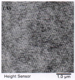
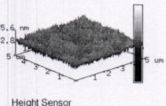
Nanoparticle-based EUV resist materials represent a promising approach for achieving sub-5 nm semiconductor nodes, yet they face significant technical challenges that must be overcome before widespread industrial implementation. The primary obstacle lies in achieving consistent nanoparticle size distribution and morphology control. Current synthesis methods struggle to produce uniform particles below 3 nm with the narrow size distribution required for high-resolution patterning, resulting in line edge roughness that compromises device performance.
Material stability presents another critical challenge, as nanoparticles tend to agglomerate during storage and processing, leading to inconsistent lithographic performance. The surface chemistry of these particles must be precisely engineered to maintain dispersion stability while preserving sensitivity to EUV radiation, creating a complex optimization problem that has not been fully resolved.
Integration of nanoparticle resists into existing semiconductor manufacturing workflows introduces additional complications. The viscosity and flow characteristics of nanoparticle suspensions differ significantly from traditional polymer resists, requiring modifications to coating equipment and processes. Furthermore, the interaction between nanoparticles and substrate surfaces can lead to non-uniform film formation and adhesion issues that impact pattern fidelity.
The radiation chemistry of nanoparticle resists presents unique challenges compared to conventional molecular or polymer systems. The mechanisms of radiation-induced chemical reactions at nanoparticle interfaces are not fully understood, making it difficult to predict and optimize sensitivity, contrast, and resolution. Additionally, secondary electron generation and scattering effects in nanoparticle systems contribute to proximity effects that limit achievable resolution.
Pattern collapse has emerged as a significant issue as feature sizes approach sub-5 nm dimensions. The high aspect ratio structures created during development experience strong capillary forces that can cause mechanical failure. Nanoparticle resists must therefore balance mechanical strength with sensitivity and resolution requirements, a trade-off that becomes increasingly difficult at smaller dimensions.
Environmental and safety considerations also pose challenges, as many high-performance nanoparticles contain heavy metals or toxic elements that raise concerns about worker exposure and environmental contamination. Developing "green" nanoparticle resist formulations that maintain performance while reducing toxicity remains an active area of research but has yet to yield commercially viable solutions.
Finally, metrology and characterization of nanoparticle resist performance present technical difficulties. Conventional techniques for measuring resist properties may not accurately capture the unique behavior of nanoparticle systems, necessitating the development of new analytical methods specifically tailored to these materials.
Current Nanoparticle-Based EUV Resist Solutions
01 Metal oxide nanoparticles for EUV resist materials
Metal oxide nanoparticles, such as hafnium oxide, zirconium oxide, and titanium oxide, are incorporated into EUV resist formulations to enhance sensitivity and resolution. These nanoparticles can absorb EUV radiation efficiently and generate secondary electrons, which increases the efficiency of the photochemical reactions in the resist. The high refractive index of metal oxide nanoparticles also contributes to improved resolution by reducing pattern collapse and enhancing contrast.- Metal oxide nanoparticles for EUV resist materials: Metal oxide nanoparticles, such as hafnium oxide, zirconium oxide, and titanium oxide, are incorporated into EUV resist formulations to enhance sensitivity and resolution. These nanoparticles can absorb EUV radiation efficiently and generate secondary electrons, improving pattern transfer. The metal oxide nanoparticles can be surface-modified to improve dispersion in the resist matrix and prevent aggregation, resulting in smoother line edges and better resolution for advanced semiconductor manufacturing.
- Hybrid organic-inorganic nanoparticle resist systems: Hybrid resist systems combine organic polymers with inorganic nanoparticles to achieve superior EUV lithographic performance. These systems leverage the high absorption cross-section of inorganic components while maintaining the processability of organic materials. The organic components typically include acid-labile groups that undergo catalytic deprotection upon exposure, while the inorganic nanoparticles enhance sensitivity and etch resistance. This combination enables high-resolution patterning with reduced line edge roughness and improved pattern fidelity at sub-10nm feature sizes.
- Core-shell nanostructures for enhanced resolution: Core-shell nanostructures feature a central core material surrounded by a shell of different composition, designed specifically for EUV lithography applications. The core typically consists of high-Z elements for enhanced EUV absorption, while the shell provides compatibility with the resist matrix and can be functionalized for specific chemical interactions. These structures enable precise control over acid generation and diffusion in chemically amplified resist systems, resulting in sharper pattern definition and higher resolution capability for next-generation semiconductor devices.
- Nanoparticle size and distribution control for resolution enhancement: The size and distribution of nanoparticles in EUV resist materials significantly impact resolution capabilities. Precisely controlled nanoparticle synthesis methods produce uniform particles with narrow size distributions, typically in the 2-10nm range, which is critical for achieving high-resolution patterns. Advanced dispersion techniques prevent agglomeration and ensure homogeneous distribution throughout the resist matrix. This control over nanoparticle characteristics enables smoother line edges, reduced roughness, and improved contrast, ultimately allowing for the patterning of smaller feature sizes in semiconductor manufacturing.
- Metal-containing nanoparticles with sensitizer compounds: Metal-containing nanoparticles combined with photosensitizer compounds create highly efficient EUV resist materials. The metal components (such as tin, antimony, or bismuth) provide strong EUV absorption, while sensitizer molecules enhance the generation and amplification of secondary reactions. This combination improves quantum efficiency in the resist system, reducing the required exposure dose while maintaining high resolution. The sensitizer compounds can be chemically bound to the nanoparticle surface or incorporated into the surrounding matrix, creating a synergistic effect that enables patterning of features below 10nm with high fidelity.
02 Hybrid organic-inorganic nanoparticle resists
Hybrid organic-inorganic nanoparticle resists combine the advantages of organic polymers and inorganic materials. The organic components provide processability and film-forming properties, while the inorganic nanoparticles enhance EUV absorption and pattern resolution. These hybrid materials often feature metal oxide cores with organic ligands or polymer shells that improve dispersion and compatibility with the resist matrix. This approach enables high-resolution patterning with reduced line edge roughness and improved etch resistance.Expand Specific Solutions03 Surface modification of nanoparticles for EUV resist integration
Surface modification of nanoparticles is crucial for their successful integration into EUV resist materials. By attaching specific functional groups to the nanoparticle surface, their dispersion in the resist matrix can be improved, preventing aggregation that would otherwise reduce resolution. Surface-modified nanoparticles can be designed to participate in acid-catalyzed reactions during the exposure and development process, enhancing sensitivity and contrast. This approach enables the creation of homogeneous resist films with controlled nanoparticle distribution.Expand Specific Solutions04 Metal-containing nanoparticles for pattern transfer enhancement
Metal-containing nanoparticles incorporated into EUV resist formulations can significantly enhance pattern transfer processes. These nanoparticles provide increased etch resistance, allowing for higher aspect ratio features and improved pattern fidelity during subsequent processing steps. The presence of metals like tin, antimony, or platinum in the nanoparticles can also enhance EUV absorption, leading to higher sensitivity and better resolution. Additionally, these materials can facilitate selective area deposition or etching processes for advanced patterning schemes.Expand Specific Solutions05 Size-controlled nanoparticles for ultra-high resolution
Precisely size-controlled nanoparticles are essential for achieving ultra-high resolution in EUV lithography. Nanoparticles with uniform size distribution below 5 nm can enable patterning of features approaching the theoretical resolution limits of EUV lithography. The small size ensures minimal impact on line edge roughness while maintaining the benefits of nanoparticle incorporation. Advanced synthesis methods allow for precise control over nanoparticle dimensions, composition, and surface chemistry, which directly impacts the achievable resolution in the final patterned structures.Expand Specific Solutions
Key Industry Players in EUV Materials
The EUV resist materials market for sub-5 nm nodes is in a growth phase, with increasing demand driven by semiconductor miniaturization trends. The competitive landscape features established chemical companies like Shin-Etsu Chemical, JSR Corp, and TOKYO OHKA KOGYO leading commercial development, while equipment manufacturers ASML and Lam Research provide complementary technologies. Academic institutions including Tsinghua University and Cornell University contribute fundamental research. The market is characterized by moderate technological maturity, with nanoparticle-based approaches showing promise but requiring further refinement for mass production. Collaboration between industry leaders and research institutions is accelerating development, with companies like FUJIFILM and IBM pursuing innovative formulations to overcome resolution and sensitivity challenges in next-generation lithography.
Shin-Etsu Chemical Co., Ltd.
Technical Solution: Shin-Etsu has developed innovative metal oxide nanoparticle-based EUV resist materials specifically designed for sub-5 nm node semiconductor manufacturing. Their approach incorporates hafnium and zirconium oxide nanoparticles (2-5 nm diameter) into hybrid organic-inorganic matrices, creating high-sensitivity resists with resolution capabilities below 5 nm. The company's proprietary surface modification technology prevents nanoparticle aggregation while maintaining uniform dispersion throughout the resist film. Their metal oxide nanoparticles demonstrate 3-4x higher EUV absorption efficiency compared to conventional chemically amplified resists (CARs), significantly reducing the required exposure dose. Shin-Etsu's formulations also incorporate novel quencher compounds that control acid diffusion, enhancing pattern fidelity and reducing line edge roughness to below 2 nm. Recent advancements include the integration of secondary electron controlling additives that minimize proximity effects in dense patterns.
Strengths: Superior EUV absorption efficiency reduces exposure dose requirements, enabling higher throughput in manufacturing. Excellent pattern fidelity with minimal line edge roughness. Weaknesses: Higher material costs compared to traditional resists. May require specialized processing equipment for optimal performance.
JSR Corp.
Technical Solution: JSR Corporation has pioneered metal-based nanoparticle EUV resist technology through their "hybrid multi-trigger resist" platform specifically targeting sub-5 nm node applications. Their approach combines metal oxide nanoparticles (primarily tin-based) with specialized polymer matrices to achieve exceptional sensitivity and resolution. JSR's proprietary nanoparticle synthesis method produces uniform 3-4 nm particles with precisely controlled size distribution, crucial for pattern uniformity at extreme dimensions. The company's resist formulations incorporate chemical amplification mechanisms alongside direct photon absorption, creating a dual-action system that improves sensitivity by approximately 30% compared to conventional single-mechanism resists. JSR has also developed specialized surface ligands for their nanoparticles that enhance compatibility with existing semiconductor processing workflows while maintaining stability during storage. Recent innovations include the incorporation of secondary reaction quenchers that significantly reduce pattern collapse in high-aspect-ratio features, enabling line patterns with widths below 8 nm and pitch below 16 nm.
Strengths: Dual-action mechanism provides excellent sensitivity while maintaining resolution. Compatible with existing semiconductor manufacturing infrastructure. Weaknesses: Potential for metal contamination requires additional process controls. Pattern collapse remains challenging at extreme dimensions despite improvements.
Critical Patents in Metal-Oxide Nanoparticle Resists
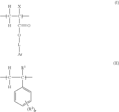
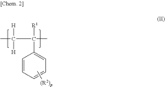
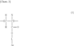
Positive resist composition for extreme ultraviolet lithography and resist pattern formation kit for extreme ultraviolet lithography
PatentPendingUS20230324797A1
Innovation
- A positive resist composition for EUV lithography is developed, comprising a copolymer with specific monomer units (A) and (B) and a weight-average molecular weight greater than 100,000, optimized to include a 1-phenyl-1-trifluoromethyl-2,2,2-trifluoroethyl α-chloroacrylate unit and α-methylstyrene unit, with a molecular weight distribution and monomer proportion that enhances sensitivity and resolution.

A new class of non-chemically amplified molecular photoresists for next generation integrated circuits (ICS) technology
PatentActiveIN201611044190A
Innovation
- Development of novel non-chemically amplified molecular resists (n-CAR) using sulfonium triflates, which are sensitive to various lithography techniques and can pattern nanostructures without the need for external photochemical entities, incorporating metal oxide nanoparticles for enhanced sensitivity and resolution.
Environmental Impact of Nanoparticle Resist Processing
The environmental impact of nanoparticle-based EUV resist processing represents a critical consideration as semiconductor manufacturing advances toward sub-5 nm nodes. These novel materials, while offering superior lithographic performance, introduce unique environmental challenges throughout their lifecycle that must be thoroughly assessed and mitigated.
Water consumption in nanoparticle resist processing significantly exceeds that of traditional resists, with estimates suggesting 30-40% higher usage primarily due to additional purification and development steps. This increased demand places strain on local water resources, particularly in semiconductor manufacturing hubs already facing water scarcity issues.
Chemical waste generation presents another substantial concern. Nanoparticle resists typically contain heavy metals such as hafnium, zirconium, or tin, which can persist in the environment if improperly managed. Studies indicate that effluent from facilities utilizing these materials may contain nanoparticle concentrations ranging from 0.5-2.0 mg/L, necessitating specialized treatment protocols beyond conventional wastewater management systems.
Energy consumption throughout the nanoparticle resist lifecycle exceeds conventional alternatives by approximately 25%, according to recent industry analyses. This increased energy footprint stems from energy-intensive synthesis processes, specialized handling requirements, and more complex post-exposure development procedures.
Air quality impacts arise primarily during nanoparticle synthesis and application processes. Potential airborne nanoparticle emissions require sophisticated filtration systems capable of capturing particles below 10 nm in diameter, representing a significant engineering challenge for fabrication facilities.
Regulatory frameworks governing nanoparticle materials remain inconsistent globally, creating compliance challenges for international semiconductor manufacturers. The European Union's REACH regulations and similar initiatives in Japan and South Korea have begun addressing nanomaterial-specific environmental concerns, while other regions lag in developing comprehensive guidelines.
Industry response has focused on developing closed-loop processing systems that recover and recycle nanoparticles from waste streams. Leading manufacturers report recovery rates approaching 70-80% for certain metal oxide nanoparticles, substantially reducing environmental discharge. Additionally, water recycling technologies specifically designed for nanoparticle contamination have demonstrated efficiency improvements of 15-20% over the past five years.
Future sustainability efforts must prioritize green chemistry approaches to nanoparticle synthesis, utilizing less toxic precursors and environmentally benign solvents. Research into biodegradable capping agents and ligands shows promise for reducing the environmental persistence of nanoparticles that escape containment systems.
Supply Chain Security for Critical EUV Materials
The security of the EUV resist materials supply chain represents a critical concern for semiconductor manufacturing, particularly for advanced nodes below 5 nm where nanoparticle-based EUV resist materials are essential. The geopolitical concentration of critical raw materials presents significant vulnerabilities that could disrupt global semiconductor production.
Currently, key materials for nanoparticle-based EUV resists, including metal oxide nanoparticles, organometallic compounds, and specialized polymers, are sourced from a limited number of countries. Japan, the United States, and Germany dominate the high-purity chemical production, while rare earth elements often originate from China. This geographic concentration creates potential single points of failure in the supply chain.
Recent disruptions, including the COVID-19 pandemic and trade tensions between major economies, have highlighted the fragility of these supply chains. Several semiconductor manufacturers experienced delays in EUV resist delivery, resulting in production slowdowns at advanced nodes. The specialized nature of these materials, with their stringent purity requirements exceeding 99.999%, further complicates alternative sourcing options.
Industry leaders have begun implementing multi-faceted strategies to enhance supply chain resilience. These include geographical diversification of suppliers, development of alternative material formulations, and increased inventory management. TSMC and Samsung have established partnerships with multiple resist suppliers across different regions, while Intel has invested in domestic production capabilities for critical materials.
Regulatory frameworks are evolving to address these vulnerabilities. The CHIPS Act in the United States and similar initiatives in Europe and Asia aim to strengthen domestic semiconductor ecosystems, including materials production. These programs provide funding for research into alternative materials that could reduce dependence on geographically concentrated resources.
Looking forward, the industry must balance just-in-time manufacturing efficiencies with supply chain security. Emerging approaches include the development of circular economy models for rare materials recovery and recycling from semiconductor manufacturing waste. Additionally, research into bio-based alternatives for certain EUV resist components shows promise for reducing dependence on traditional chemical supply chains.
The establishment of industry consortia focused specifically on EUV materials security represents another positive development. Organizations like SEMI and IMEC have created working groups dedicated to supply chain risk assessment and mitigation strategies, fostering collaboration between material suppliers, equipment manufacturers, and semiconductor companies to ensure continued innovation without compromising security.
Unlock deeper insights with Patsnap Eureka Quick Research — get a full tech report to explore trends and direct your research. Try now!
Generate Your Research Report Instantly with AI Agent
Supercharge your innovation with Patsnap Eureka AI Agent Platform!