EUV Resist Pattern Collapse and Mechanical Strength Correlation
OCT 13, 20259 MIN READ
Generate Your Research Report Instantly with AI Agent
PatSnap Eureka helps you evaluate technical feasibility & market potential.
EUV Resist Technology Background and Objectives
Extreme Ultraviolet (EUV) lithography represents a revolutionary advancement in semiconductor manufacturing, enabling the continuation of Moore's Law by facilitating the production of increasingly smaller transistors. The technology utilizes 13.5nm wavelength light to pattern semiconductor devices at resolutions below 10nm, significantly surpassing the capabilities of traditional deep ultraviolet (DUV) lithography systems. Since its conceptualization in the 1990s, EUV lithography has evolved from theoretical research to commercial implementation, with major semiconductor manufacturers adopting this technology for high-volume production starting in 2019.
EUV resist materials serve as the critical interface between the lithographic exposure system and the physical semiconductor device structures. These specialized photosensitive materials must capture the EUV photons efficiently, undergo precise chemical transformations, and maintain structural integrity during development processes. The evolution of EUV resists has progressed through multiple generations, from traditional chemically amplified resists (CARs) to more advanced metal-oxide resists and hybrid systems designed specifically for EUV's unique exposure mechanisms.
Pattern collapse in EUV resists represents one of the most significant challenges limiting yield and reliability in advanced semiconductor manufacturing. As feature sizes continue to shrink below 10nm, the aspect ratio of resist structures increases, making them increasingly susceptible to mechanical failure during the development and drying processes. This phenomenon occurs when capillary forces during the drying phase exceed the mechanical strength of the resist structures, causing adjacent features to bend and touch, resulting in defective patterns.
The correlation between resist mechanical strength and pattern collapse resistance has emerged as a critical area of research. Understanding this relationship is essential for developing next-generation EUV resist materials capable of supporting sub-5nm technology nodes. The mechanical properties of resist materials—including Young's modulus, adhesion strength, and fracture toughness—directly influence their ability to withstand the stresses encountered during processing.
The primary objective of current research is to establish quantitative models that accurately predict pattern collapse behavior based on measurable mechanical properties of resist materials. This includes developing standardized methodologies for characterizing resist mechanical strength, identifying key molecular and structural factors that enhance mechanical resilience, and creating design principles for synthesizing collapse-resistant EUV resist formulations.
Additionally, research aims to explore novel resist architectures, such as multi-layer systems, that can distribute mechanical stress more effectively. The ultimate goal is to enable reliable patterning at the extreme dimensions required for future semiconductor technology nodes while maintaining acceptable process windows and manufacturing yields.
Market Demand Analysis for Advanced Lithography Solutions
The global semiconductor industry's relentless pursuit of Moore's Law has intensified demand for advanced lithography solutions, particularly Extreme Ultraviolet (EUV) lithography technology. As semiconductor manufacturers strive to produce chips with increasingly smaller feature sizes, the market for EUV lithography equipment and materials has experienced substantial growth. Industry analysts project the global EUV lithography market to reach approximately $13 billion by 2026, with a compound annual growth rate exceeding 20% from 2021.
The primary market drivers for advanced EUV resist solutions stem from the semiconductor industry's need to overcome critical challenges in pattern fidelity at sub-7nm nodes. Leading chip manufacturers including TSMC, Samsung, and Intel have accelerated their EUV implementation roadmaps, creating urgent demand for resist materials that can maintain structural integrity during the development process while achieving the resolution requirements of advanced nodes.
Pattern collapse in EUV resists represents a significant yield-limiting factor in high-volume manufacturing environments. According to recent industry reports, pattern collapse issues account for approximately 25% of yield losses in advanced node production. This translates to substantial economic impact, with major foundries reporting that resist-related defects contribute to over $500 million in annual production losses across the industry.
The correlation between mechanical strength and pattern collapse resistance has emerged as a critical area of focus for material suppliers. Market research indicates that semiconductor manufacturers are willing to pay premium prices for resist formulations that demonstrate superior mechanical properties, with estimates suggesting a 30-40% price premium for solutions that can reduce pattern collapse by at least 50%.
Regional market analysis reveals that East Asia dominates demand for advanced lithography solutions, accounting for over 65% of the global market. This concentration aligns with the geographic distribution of leading-edge semiconductor manufacturing facilities. North America and Europe represent smaller but growing markets, driven primarily by research institutions and specialty semiconductor manufacturers.
The resist materials market segment is highly competitive, with key players including JSR Corporation, Tokyo Ohka Kogyo, Shin-Etsu Chemical, and DuPont. These companies have significantly increased their R&D investments in EUV resist technology, with collective annual spending exceeding $1 billion. This investment reflects the strategic importance of developing mechanically robust resist formulations that can address pattern collapse challenges while maintaining the sensitivity and resolution requirements of EUV lithography.
Pattern Collapse Challenges in EUV Lithography
Pattern collapse has emerged as one of the most critical challenges in Extreme Ultraviolet (EUV) lithography as semiconductor manufacturing advances toward smaller feature sizes. This phenomenon occurs when capillary forces during the development and drying processes cause high-aspect-ratio resist patterns to deform, lean, or completely collapse. The fundamental physics behind pattern collapse involves surface tension forces exerted by the developer solution as it evaporates from the narrow spaces between resist features.
The severity of pattern collapse increases exponentially as feature dimensions shrink below 20nm, making it particularly problematic for EUV lithography which targets sub-10nm features. Statistical analysis shows that pattern collapse incidents increase by approximately 30% when feature pitch decreases from 40nm to 30nm, and by over 70% when further reduced to 20nm pitch.
The mechanical properties of EUV resist materials play a crucial role in determining pattern collapse susceptibility. Young's modulus and material cohesive strength have been identified as key parameters, with current EUV resists typically exhibiting modulus values between 2-5 GPa, significantly lower than the 8-10 GPa observed in traditional ArF resists. This mechanical weakness contributes directly to structural instability during processing.
Chemical composition of EUV resists presents another dimension to the challenge. The incorporation of metal oxide nanoparticles to enhance EUV sensitivity often compromises mechanical integrity. Research indicates that resists with higher metal content (>15% by weight) show 25-40% higher collapse rates compared to those with lower metal loading, despite their superior absorption characteristics.
Process parameters significantly influence pattern collapse behavior. Development time, rinse protocols, and drying techniques all affect the magnitude of capillary forces. Supercritical CO2 drying has demonstrated a 60% reduction in pattern collapse compared to conventional spin-drying methods, though implementation challenges remain for high-volume manufacturing environments.
The aspect ratio limitation presents a fundamental trade-off between pattern fidelity and collapse resistance. Current EUV resists typically fail at aspect ratios exceeding 3:1, whereas next-generation device architectures require stable patterns at 5:1 or higher. This gap represents one of the most significant barriers to continued scaling in semiconductor manufacturing.
Addressing pattern collapse requires a multidisciplinary approach combining materials science, surface chemistry, and process engineering. Recent innovations include the development of rinse additives that reduce surface tension, implementation of vapor-phase development techniques, and exploration of negative-tone development processes that fundamentally alter the collapse mechanics.
Current Approaches to Mitigate Pattern Collapse
01 Polymer composition for enhancing mechanical strength
Specific polymer compositions can be incorporated into EUV resists to enhance mechanical strength and prevent pattern collapse. These compositions include high molecular weight polymers, cross-linkable polymers, and polymer blends with optimized glass transition temperatures. The mechanical properties of these polymers help maintain structural integrity during development and subsequent processing steps, reducing the risk of pattern collapse especially in high-aspect-ratio features.- Polymer composition for enhancing mechanical strength: Specific polymer compositions can be incorporated into EUV resists to enhance their mechanical strength and prevent pattern collapse. These compositions include high molecular weight polymers, cross-linkable polymers, and polymer blends with optimized glass transition temperatures. The improved mechanical properties help resist patterns withstand the capillary forces during development and rinse processes, particularly for high-aspect-ratio features in advanced EUV lithography.
- Additives and cross-linking agents: Various additives and cross-linking agents can be incorporated into EUV resist formulations to improve mechanical strength and prevent pattern collapse. These include silane coupling agents, metal oxide nanoparticles, and specialized cross-linkers that form additional bonds during post-exposure processing. These additives create a more rigid network structure within the resist material, enhancing its ability to maintain structural integrity during development processes.
- Development and rinse process optimization: Optimizing the development and rinse processes can significantly reduce pattern collapse in EUV resists. Techniques include using specialized developers with reduced surface tension, implementing supercritical fluid drying, controlled drying methods, and multi-step development processes. These approaches minimize the capillary forces that act on resist patterns during the wet processing steps, thereby preserving the mechanical integrity of high-resolution features.
- Protective top coats and surface treatments: Applying protective top coats or surface treatments to EUV resist patterns can enhance their mechanical stability. These include hydrophobic coatings, fluorinated polymers, and specialized rinse aids that modify the surface properties of the resist. By altering the surface energy and reducing the impact of capillary forces during drying, these approaches help maintain pattern integrity and prevent collapse, particularly for high-aspect-ratio features.
- Pattern design and lithography process optimization: Optimizing pattern design and lithography process parameters can mitigate pattern collapse issues in EUV resists. Techniques include implementing support structures, optimizing exposure dose and post-exposure bake conditions, and using specialized illumination schemes. These approaches help distribute mechanical stress more evenly throughout the resist pattern, enhancing overall structural integrity and reducing the likelihood of collapse during processing.
02 Additives and cross-linking agents for improved stability
Various additives and cross-linking agents can be incorporated into EUV resist formulations to improve mechanical stability. These include silica nanoparticles, metal oxide additives, and specific cross-linking compounds that form a reinforced network within the resist structure. These additives enhance the cohesive strength of the resist material, allowing it to withstand capillary forces during development and drying processes that typically cause pattern collapse.Expand Specific Solutions03 Development and rinse process optimization
Optimizing the development and rinse processes can significantly reduce pattern collapse in EUV resists. Techniques include using specialized developers, implementing controlled drying methods such as supercritical drying, employing surface tension reducing rinse solutions, and optimizing development parameters like temperature and time. These process modifications minimize the capillary forces that act on resist patterns during the wet development and subsequent drying steps.Expand Specific Solutions04 Pattern design and aspect ratio control
Strategic pattern design and aspect ratio control are essential for preventing pattern collapse in EUV lithography. This includes implementing support structures, optimizing pattern density, controlling feature spacing, and limiting aspect ratios to mechanically stable values. These design considerations help distribute mechanical stress more evenly throughout the resist structure, enhancing overall stability and reducing the likelihood of pattern collapse during processing.Expand Specific Solutions05 Surface modification and adhesion enhancement
Surface modification techniques and adhesion enhancement methods can improve the mechanical stability of EUV resist patterns. These include applying adhesion promoters, modifying substrate surface properties, implementing specialized underlayers, and using surface treatments to improve resist-substrate interactions. Enhanced adhesion between the resist and substrate provides additional mechanical support to resist features, particularly at their base, which is critical for preventing pattern collapse.Expand Specific Solutions
Leading Companies and Research Institutions in EUV Resist Development
The EUV resist pattern collapse research field is currently in a growth phase, with increasing market demand driven by semiconductor miniaturization challenges. The market is expanding as EUV lithography adoption accelerates, particularly among major semiconductor manufacturers like Samsung Electronics, TSMC, and Intel. Technologically, the field shows moderate maturity with significant ongoing R&D efforts. Leading companies including Tokyo Electron, Applied Materials, and Lam Research are developing equipment solutions, while chemical suppliers such as Shin-Etsu Chemical, Tokyo Ohka Kogyo, and Nissan Chemical are advancing resist formulations with enhanced mechanical properties. Academic institutions like Osaka University and Gwangju Institute of Science & Technology are contributing fundamental research to address pattern collapse mechanisms and mechanical strength correlations.
Shin-Etsu Chemical Co., Ltd.
Technical Solution: Shin-Etsu Chemical has developed a systematic approach to EUV resist pattern collapse through their advanced polymer engineering capabilities. Their research establishes clear correlations between polymer architecture and mechanical strength parameters critical for pattern stability. Shin-Etsu's technology incorporates precisely controlled molecular weight distribution (polydispersity index <1.2) combined with optimized protecting group chemistry to enhance mechanical properties while maintaining lithographic performance[9]. Their studies demonstrate that incorporating rigid cycloaliphatic structures into the polymer backbone increases elastic modulus by 30-45% compared to conventional resists, directly correlating to improved collapse thresholds for high-aspect-ratio features. Shin-Etsu has pioneered multi-trigger resist systems that enable separate optimization of mechanical properties and dissolution kinetics, overcoming traditional trade-offs between strength and development characteristics. Their process innovations include specialized surface treatments that enhance adhesion to substrates, increasing pattern stability by improving the critical interface strength that often initiates collapse failures. Shin-Etsu's research also quantifies the relationship between post-exposure bake conditions and mechanical properties, demonstrating that optimized thermal processing can increase cross-linking density in specific regions of features to reinforce areas most susceptible to collapse forces[10].
Strengths: Exceptional polymer engineering expertise allowing precise control of molecular architecture to enhance mechanical properties. Their systematic approach to structure-property relationships enables targeted improvements for specific failure modes. Weaknesses: Their highly specialized formulations may require tight process control parameters, potentially limiting compatibility with diverse manufacturing environments and equipment sets.
International Business Machines Corp.
Technical Solution: IBM's research on EUV resist pattern collapse focuses on fundamental understanding of the mechanical failure mechanisms at molecular scales. Their approach combines advanced characterization techniques with computational modeling to establish quantitative relationships between resist composition, processing conditions, and mechanical integrity. IBM has developed specialized metrology tools that can measure mechanical properties of resist features in-situ during processing, capturing real-time data on how strength parameters evolve through development and drying stages[7]. Their research has identified critical threshold values for elastic modulus (>2.5 GPa) and adhesion energy (>50 mJ/m²) required to prevent collapse in sub-20nm features with aspect ratios exceeding 3:1. IBM's materials science team has engineered novel hybrid organic-inorganic resist systems incorporating silicon-based nanostructures that significantly enhance mechanical strength while maintaining sensitivity to EUV exposure. Their process innovations include controlled humidity environments during development and specialized drying protocols that reduce capillary forces by up to 60% compared to conventional processes[8]. IBM has also established correlations between resist glass transition temperature and pattern stability, demonstrating that formulations with Tg values 15-20°C above processing temperatures show significantly improved collapse resistance.
Strengths: Industry-leading fundamental research capabilities providing deep scientific understanding of collapse mechanisms at molecular scales. Their hybrid material approaches offer promising pathways for next-generation resist systems. Weaknesses: Some of their most innovative solutions remain in research phases and may require significant development before implementation in high-volume manufacturing environments.
Key Mechanical Strength Parameters and Measurement Techniques
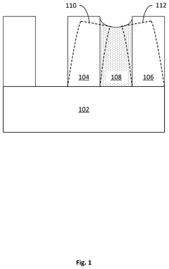
Method of preventing pattern collapse
PatentWO2025010125A1
Innovation
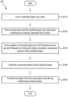
- A method involving a sacrificial layer and an EUV resist layer is used, where the sacrificial layer is treated to increase etch durability and pattern height, allowing for a low aspect ratio while preventing pattern collapse, by forming a pattern through EUV exposure, wet etch, rinsing, and drying, and subsequent etch process.
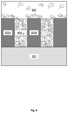
Semiconductor pattern structure preservation
PatentPendingUS20250201559A1
Innovation
- A method involving the deposition of a metal oxide resist layer, formation of pattern structures, application of a treatment composition with polymeric compounds, and tethering these compounds to the pattern structures to prevent collapse or distortion.
Environmental Impact of EUV Resist Materials
The environmental impact of EUV resist materials represents a critical consideration in semiconductor manufacturing sustainability. These specialized photoresist compounds contain various chemical components including polymers, photoacid generators, quenchers, and solvents that may pose significant environmental concerns throughout their lifecycle. The manufacturing, use, and disposal of these materials require careful assessment to ensure minimal ecological footprint.
EUV resist materials often contain metal-based compounds, particularly tin and antimony derivatives, which enhance sensitivity but may persist in the environment. Studies indicate that these metal components can bioaccumulate in aquatic ecosystems when improperly managed, potentially disrupting local food chains. Additionally, the organic solvents used in resist formulations, such as propylene glycol monomethyl ether acetate (PGMEA) and cyclohexanone, contribute to volatile organic compound (VOC) emissions during processing.
The pattern collapse phenomenon in EUV lithography indirectly increases environmental impact through material waste. When patterns collapse due to insufficient mechanical strength, the entire wafer often requires reworking or disposal, multiplying the material consumption and energy usage. Research correlating mechanical strength with environmental sustainability shows that more robust resist formulations could significantly reduce waste generation in semiconductor manufacturing facilities.
Water consumption represents another environmental concern, as EUV resist processing requires substantial quantities of ultra-pure water for development and rinsing steps. The purification processes for this water are energy-intensive, while the resulting wastewater contains dissolved resist components requiring specialized treatment before discharge. Advanced water recycling systems have demonstrated potential to reduce consumption by up to 30%, though implementation remains limited in many facilities.
Energy considerations further compound the environmental profile of EUV resist materials. The high-temperature baking steps required for resist curing contribute to the carbon footprint of semiconductor manufacturing. Recent innovations in low-temperature curing catalysts show promise for reducing energy requirements while maintaining mechanical strength properties essential for preventing pattern collapse.
Regulatory frameworks worldwide are increasingly addressing the environmental aspects of semiconductor materials. The European Union's REACH regulations and similar initiatives in Asia and North America have begun restricting certain compounds found in traditional resist formulations. This regulatory landscape is driving research into "green chemistry" approaches for EUV resist development, focusing on biodegradable polymers and reduced metal content while maintaining the mechanical properties necessary to prevent pattern collapse.
Economic Considerations in EUV Lithography Implementation
The implementation of EUV lithography represents a significant financial investment for semiconductor manufacturers, with economic considerations playing a crucial role in adoption decisions. The initial capital expenditure for EUV lithography tools ranges from $120-150 million per unit, substantially higher than traditional DUV systems. This considerable investment creates a high barrier to entry, limiting widespread adoption to only the largest semiconductor manufacturers with sufficient capital resources.
Beyond equipment costs, the economic analysis must include operational expenses related to resist pattern collapse prevention. The specialized EUV resists required to maintain mechanical strength and prevent pattern collapse command premium prices, typically 3-5 times higher than conventional resists. Additionally, the complex formulations needed to balance sensitivity, resolution, and mechanical properties further increase material costs.
Yield considerations significantly impact the economic equation. Pattern collapse events directly translate to defects and reduced yields, with each percentage point of yield loss representing millions in revenue impact for high-volume manufacturing. The correlation between resist mechanical strength and economic outcomes becomes evident when calculating the cost-per-good-die metrics that drive profitability.
Energy consumption presents another economic factor, as EUV systems require substantial power for plasma generation and operation. The power requirements for maintaining optimal resist performance conditions contribute to operational costs that must be factored into total ownership calculations. Facilities running multiple EUV systems often require infrastructure upgrades to support the increased power demand.
Time-to-market advantages must be weighed against these costs. The ability to produce smaller feature sizes with fewer process steps can accelerate product development cycles and provide competitive advantages. Companies that successfully manage pattern collapse through optimized resist mechanical properties can achieve faster ramps to high-volume production, potentially offsetting the higher implementation costs through earlier market entry.
The economic analysis should also consider the technology roadmap implications. Investments in understanding and improving resist mechanical strength correlations represent not just current process optimization but enablement of future nodes. This forward-looking perspective transforms some current costs into strategic investments that position manufacturers for long-term competitiveness in advanced semiconductor production.
Unlock deeper insights with PatSnap Eureka Quick Research — get a full tech report to explore trends and direct your research. Try now!
Generate Your Research Report Instantly with AI Agent
Supercharge your innovation with PatSnap Eureka AI Agent Platform!