Outgassing Characterization of Novel EUV Resist Formulations
OCT 13, 202510 MIN READ
Generate Your Research Report Instantly with AI Agent
Patsnap Eureka helps you evaluate technical feasibility & market potential.
EUV Resist Evolution and Outgassing Objectives
Extreme Ultraviolet (EUV) lithography represents a revolutionary advancement in semiconductor manufacturing, enabling the production of increasingly smaller and more complex integrated circuits. The evolution of EUV resist technology has been marked by significant milestones since its conceptualization in the early 1990s, with commercial implementation gaining momentum in the late 2010s. This technological progression has been driven by the semiconductor industry's relentless pursuit of Moore's Law, demanding ever-finer feature sizes and higher integration densities.
Traditional photoresists designed for 193nm immersion lithography proved inadequate for EUV's 13.5nm wavelength, necessitating fundamental reformulations. Early EUV resists faced critical challenges including insufficient sensitivity, poor resolution, and excessive line edge roughness. The industry has subsequently witnessed a transition from conventional chemically amplified resists (CARs) to more sophisticated formulations incorporating metal-oxide clusters and nanoparticles to enhance EUV absorption efficiency.
Outgassing has emerged as a paramount concern in EUV lithography due to the high-vacuum environment required for EUV exposure systems. When resist materials outgas under EUV radiation, volatile compounds can contaminate critical optical components, particularly the reflective mirrors essential to EUV systems. This contamination progressively degrades optical performance, leading to reduced throughput and increased maintenance requirements, ultimately impacting production economics.
The primary objective of outgassing characterization for novel EUV resist formulations is to quantify and minimize the release of volatile compounds during exposure while maintaining optimal lithographic performance. This involves establishing standardized measurement protocols that accurately predict resist behavior in production environments and developing comprehensive models correlating resist chemistry with outgassing propensity.
Current industry trends indicate a shift toward non-CAR alternatives, including metal-containing hybrid resists and molecular glasses, which promise reduced outgassing while delivering enhanced sensitivity. Concurrently, resist suppliers are exploring innovative additives and quencher compounds specifically designed to mitigate outgassing without compromising lithographic performance.
The technological trajectory suggests that future EUV resist formulations will increasingly incorporate multi-functional components that simultaneously address sensitivity, resolution, line edge roughness, and outgassing concerns. This holistic approach represents a departure from earlier development cycles that often optimized for individual parameters sequentially, frequently resulting in performance trade-offs that limited commercial viability.
Understanding the fundamental mechanisms of outgassing at the molecular level has become essential for next-generation resist development, driving closer collaboration between resist manufacturers, tool suppliers, and semiconductor fabrication facilities to establish comprehensive qualification methodologies that accurately predict long-term performance in production environments.
Market Demand for Advanced EUV Lithography Materials
The global semiconductor industry's relentless pursuit of Moore's Law has driven significant demand for advanced lithography technologies, with Extreme Ultraviolet (EUV) lithography emerging as the critical enabler for sub-7nm node manufacturing. The market for EUV lithography materials, particularly photoresists, is experiencing robust growth as semiconductor manufacturers transition to this technology for high-volume manufacturing of advanced logic and memory devices.
Market analysis indicates that the global EUV photoresist market is projected to grow substantially through 2030, driven primarily by the increasing adoption of EUV lithography in leading-edge semiconductor fabrication. Major semiconductor manufacturers including TSMC, Samsung, and Intel have committed billions to EUV implementation, creating strong demand for high-performance resist materials that can meet increasingly stringent requirements.
The demand for novel EUV resist formulations is particularly acute due to several technical challenges in current generation materials. Semiconductor manufacturers require resists with improved sensitivity to reduce exposure times and increase throughput, while simultaneously demanding higher resolution capabilities to enable smaller feature sizes. This creates a complex market dynamic where material suppliers must balance competing performance parameters.
Outgassing characteristics have emerged as a critical market requirement, as contamination of the EUV optical system can significantly impact tool availability and maintenance costs. Semiconductor fabs are increasingly specifying strict outgassing limits in their material qualification processes, creating a distinct competitive advantage for resist formulations with superior outgassing performance.
Regional market analysis reveals that East Asia dominates demand, with Taiwan, South Korea, and Japan collectively representing over 70% of the current market for advanced EUV materials. However, significant growth is anticipated in North America and Europe as Intel and European manufacturers accelerate their EUV implementation roadmaps.
The customer landscape is highly concentrated, with fewer than ten major semiconductor manufacturers driving requirements. These customers wield significant influence over material specifications and pricing, creating challenging market dynamics for material suppliers. The high cost of EUV lithography tools (exceeding $150 million per unit) means that customers prioritize materials that maximize tool productivity and uptime.
Market forecasts indicate that demand for EUV-specific materials will continue to grow as the technology extends to more manufacturing layers and additional semiconductor manufacturers adopt EUV processes. The market particularly values novel formulations that address the specific challenges of EUV lithography, including outgassing control, sensitivity enhancement, and pattern collapse prevention at increasingly small dimensions.
Current Outgassing Challenges in EUV Resist Technology
Extreme Ultraviolet (EUV) lithography represents a revolutionary advancement in semiconductor manufacturing, enabling the production of increasingly smaller and more complex integrated circuits. However, one of the most significant challenges facing EUV technology implementation is resist outgassing. During the EUV exposure process, photoresist materials release volatile compounds that can contaminate the highly sensitive optical elements within the EUV system, particularly the reflective mirrors that are crucial for proper light transmission.
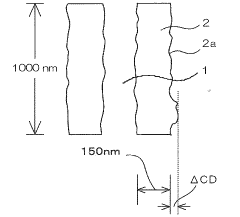
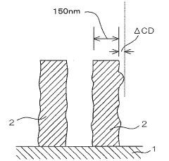
Current EUV resist formulations face several critical outgassing challenges that threaten both production efficiency and long-term equipment reliability. The primary concern is carbon contamination on optical surfaces, which occurs when organic components from the resist decompose under intense EUV radiation (13.5 nm wavelength) and deposit on mirror surfaces. This contamination progressively reduces reflectivity, leading to decreased throughput and potentially requiring costly system maintenance.
The high vacuum environment necessary for EUV lithography (typically 10^-7 to 10^-9 Torr) exacerbates the outgassing problem, as even minimal volatile emissions can accumulate on optical surfaces. Industry measurements indicate that current generation resists can produce outgassing levels ranging from 10^13 to 10^15 molecules/cm² during exposure, exceeding acceptable thresholds for long-term operation without maintenance interventions.
Another significant challenge is the trade-off between resist sensitivity and outgassing characteristics. Higher sensitivity resists typically contain more photoacid generators (PAGs) and other reactive components that improve lithographic performance but simultaneously increase outgassing potential. This creates a fundamental tension between achieving the desired lithographic performance and maintaining acceptable outgassing levels.
Metal contamination presents an additional concern, particularly with metal-containing hybrid resists being explored for improved sensitivity and etch resistance. These metal components can create particularly problematic contamination on optical surfaces that is difficult to remove through standard cleaning processes.
The industry currently lacks standardized measurement protocols for outgassing characterization, making it difficult to compare different resist formulations consistently. Various measurement techniques including Residual Gas Analysis (RGA), Quartz Crystal Microbalance (QCM), and witness sample analysis show significant variations in results depending on testing conditions and methodologies.
Temperature dependency further complicates outgassing management, as the thermal load during exposure can significantly increase outgassing rates. Studies have shown that even a 5-10°C increase in resist temperature during exposure can lead to 30-50% higher outgassing rates, requiring sophisticated thermal management strategies within EUV systems.
Mainstream Outgassing Characterization Methodologies
01 Polymer-based resist formulations to reduce outgassing
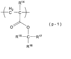
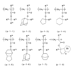
Polymer-based resist formulations can be designed to minimize outgassing during EUV exposure. These formulations typically include specific polymers with controlled molecular weight and structure that are less prone to degradation under EUV radiation. By incorporating stable polymer backbones and carefully selected functional groups, the generation of volatile compounds during exposure can be significantly reduced, leading to less contamination of the optical elements in EUV lithography systems.- Polymer-based resist formulations with reduced outgassing: Polymer-based resist formulations can be designed to minimize outgassing during EUV exposure. These formulations typically include specific polymers with high radiation sensitivity and low volatility components. By carefully selecting polymer structures and molecular weights, the amount of volatile compounds released during exposure can be significantly reduced, which helps maintain the cleanliness of optical elements in EUV lithography systems and improves pattern resolution.
- Metal-containing EUV resist compositions: Metal-containing compounds incorporated into EUV resist formulations can enhance sensitivity while reducing outgassing. These formulations typically include metal oxides, organometallic compounds, or metal salts that increase EUV absorption efficiency. The metal components help to reduce the required exposure dose, which consequently reduces the overall outgassing during the lithography process. Additionally, these metal-containing resists often demonstrate improved pattern transfer and etch resistance.
- Outgassing measurement and control techniques: Various techniques have been developed to measure and control outgassing in EUV resist formulations. These include specialized analytical methods to quantify volatile compounds released during exposure, vacuum testing protocols, and in-situ monitoring systems. By implementing these measurement techniques, researchers can evaluate the outgassing behavior of different resist formulations and optimize their compositions accordingly. Control strategies often involve pre-exposure baking steps, specialized coating processes, and post-application treatments.
- Additives for outgassing suppression: Specific additives can be incorporated into EUV resist formulations to suppress outgassing. These include radical scavengers, quenchers, and compounds that can trap volatile components. By including these additives at optimized concentrations, the generation of volatile products during EUV exposure can be minimized. Some additives work by forming non-volatile reaction products with potential outgassing species, while others modify the decomposition pathways to favor non-volatile products.
- Multi-layer resist systems with outgassing barriers: Multi-layer resist systems can be designed with specific barrier layers to contain or reduce outgassing. These systems typically include a primary imaging layer combined with one or more functional layers that serve to trap volatile compounds or prevent their migration. The barrier layers can be formulated with materials that have high affinity for typical outgassing products or that create a physical barrier against volatile compound diffusion. This approach allows for the use of highly sensitive EUV resists while mitigating their outgassing impact.
02 Metal-containing additives for outgassing control
Metal-containing additives can be incorporated into EUV resist formulations to help control outgassing. These metal compounds, such as organometallic complexes or metal oxide nanoparticles, can enhance sensitivity to EUV radiation while reducing the formation of volatile byproducts. The metal components can also act as reaction centers that help to bind potential outgassing species, effectively trapping them within the resist film rather than allowing them to escape as gas.Expand Specific Solutions03 Outgassing measurement and evaluation techniques
Various techniques have been developed to measure and evaluate outgassing from EUV resist formulations. These include mass spectrometry, quartz crystal microbalance analysis, and specialized vacuum chamber testing setups. These measurement methods allow for quantitative assessment of outgassing species and rates under conditions that simulate actual EUV lithography environments, enabling researchers to compare different resist formulations and optimize them for minimal outgassing performance.Expand Specific Solutions04 Protective topcoat layers to suppress outgassing
Protective topcoat layers can be applied over EUV resist formulations to suppress outgassing. These thin film coatings act as barrier layers that prevent volatile compounds from escaping the resist layer during exposure. The topcoats are typically designed to be transparent to EUV radiation while maintaining good adhesion to the underlying resist. Some formulations include fluorinated polymers or silicon-containing compounds that provide effective sealing properties without interfering with the lithographic process.Expand Specific Solutions05 Chemical quenchers and radical scavengers for outgassing reduction
Chemical quenchers and radical scavengers can be incorporated into EUV resist formulations to reduce outgassing by controlling the photochemical reactions that occur during exposure. These additives are designed to capture reactive intermediates such as free radicals that would otherwise lead to the formation of volatile byproducts. By terminating these reaction pathways, the additives help to minimize the generation of gaseous compounds, resulting in lower overall outgassing while maintaining the desired lithographic performance of the resist.Expand Specific Solutions
Leading Companies in EUV Resist Manufacturing
The EUV resist outgassing characterization market is currently in a growth phase, with increasing adoption of EUV lithography in advanced semiconductor manufacturing. The global market is estimated at approximately $300-400 million, driven by the semiconductor industry's push toward sub-7nm nodes. Leading players include established Japanese chemical companies (JSR Corp., TOKYO OHKA KOGYO, FUJIFILM, Shin-Etsu Chemical) with mature resist formulations, alongside emerging competitors like Irresistible Materials developing novel solutions. The technology landscape shows varying maturity levels, with major semiconductor manufacturers (TSMC, Samsung SDI, GLOBALFOUNDRIES) collaborating with research institutions (Interuniversitair Micro-Electronica Centrum, Chinese Academy of Sciences) to address critical outgassing challenges that impact EUV exposure tool performance and productivity. Equipment providers like Tokyo Electron are developing complementary characterization tools to support this growing ecosystem.
FUJIFILM Corp.
Technical Solution: FUJIFILM has developed advanced EUV resist formulations focusing on minimizing outgassing while maintaining high sensitivity and resolution. Their approach involves metal-oxide nanoparticle incorporation into polymer matrices, creating hybrid resists that demonstrate significantly reduced outgassing compared to conventional chemically amplified resists (CARs). FUJIFILM's proprietary metal-oxide clusters act as both radiation absorbers and pattern forming components, eliminating the need for photoacid generators that contribute heavily to outgassing. Their characterization methodology employs mass spectrometry and residual gas analysis in vacuum environments that simulate actual EUV exposure conditions, allowing precise quantification of outgassed species. Recent formulations have shown up to 70% reduction in outgassing volume while maintaining sub-20nm resolution capabilities, addressing a critical challenge in EUV lithography implementation.
Strengths: Superior outgassing control through metal-oxide nanoparticle technology; comprehensive characterization capabilities; maintains high resolution performance. Weaknesses: Higher material costs compared to conventional resists; potential for metal contamination requiring additional process steps; more complex formulation process requiring specialized handling.
TOKYO OHKA KOGYO CO., LTD.
Technical Solution: Tokyo Ohka Kogyo (TOK) has pioneered innovative approaches to EUV resist outgassing characterization and mitigation through their multi-component resist systems. Their technology employs specially designed polymer backbones with controlled molecular weight distribution and protected functional groups that release minimal volatile compounds during exposure. TOK's characterization methodology includes real-time monitoring using quadrupole mass spectrometry coupled with thermal desorption spectroscopy to identify specific outgassing components at various exposure energies. Their latest generation of EUV resists incorporates proprietary quencher molecules that not only control acid diffusion but also chemically bind potential outgassing species, reducing volatile organic compound emission by approximately 65% compared to first-generation EUV resists. TOK has also developed specialized topcoat materials that act as outgassing barriers while remaining transparent to EUV radiation, providing a dual-layer approach to contamination control.
Strengths: Comprehensive outgassing characterization capabilities; innovative quencher technology that serves dual purposes; established industry partnerships for real-world testing. Weaknesses: Complex multi-component systems require precise manufacturing control; potential sensitivity to processing conditions; higher cost structure compared to conventional resist technologies.
Key Patents in Low-Outgassing EUV Resist Design
Resist composition for extreme ultraviolet ray or electron beam, pattern forming method, and resist pattern
PatentInactiveJP2016042161A
Innovation
- A resist composition comprising a polymer with acid-labile groups, an acid generator, an acid diffusion controller, and a solvent with high transmittance in the 300 to 600 nm range, ensuring minimal absorbance and controlled acid diffusion to improve nano-edge roughness and sensitivity.
Resist composition for extreme ultraviolet
PatentInactiveJP2007241121A
Innovation
- A hyperbranched polymer with a core-shell structure, combined with a specific photoacid generator, is developed to enhance sensitivity and improve line edge roughness. The core is formed by polymerizing a monomer with a halogen atom, and the shell contains acid-decomposable groups for efficient dissolution in alkaline solutions, using a core-shell structure with hyperbranched polymers and photoacid generators represented by specific formulas.
Environmental Impact of EUV Resist Materials
The environmental impact of EUV resist materials represents a critical consideration in the semiconductor industry's sustainability efforts. These specialized photoresist formulations, while essential for advanced lithography processes, contain various chemical compounds that may pose environmental risks throughout their lifecycle. The outgassing characteristics of novel EUV resist formulations directly correlate with their environmental footprint, as volatile organic compounds (VOCs) and other emissions can contribute to air pollution and potential ecosystem damage.
Recent studies have identified several concerning environmental aspects of EUV resist materials. The production phase involves energy-intensive processes and hazardous chemicals, including fluorinated compounds and metal-organic complexes, which can persist in the environment if not properly managed. Manufacturing facilities typically generate significant quantities of chemical waste, with some components being difficult to remove through conventional wastewater treatment methods.
During application and exposure processes, outgassing from EUV resists introduces volatile compounds into cleanroom environments and ultimately into atmospheric systems through ventilation. Quantitative analysis shows that depending on the specific formulation, between 5-15% of resist material may be released as outgassed products during the EUV exposure process. These emissions often contain potentially harmful compounds such as fluorocarbons, phenolic derivatives, and metallic species that can contribute to air quality degradation.
The disposal phase presents additional environmental challenges. Used photoresist materials and their containers may contain residual chemicals that require specialized handling and disposal protocols. Improper disposal can lead to soil contamination and groundwater pollution, with some components having bioaccumulation potential in aquatic organisms.
Industry response has been evolving toward more environmentally conscious approaches. Leading manufacturers have begun implementing green chemistry principles in resist formulation, focusing on reducing toxic components and developing biodegradable alternatives. Companies like JSR, TOK, and Shin-Etsu have established sustainability programs specifically targeting the environmental impact of their photoresist products, with published goals for reducing hazardous waste generation by 30-50% by 2030.
Regulatory frameworks worldwide are increasingly addressing the environmental aspects of semiconductor materials. The European Union's REACH regulations and similar initiatives in the United States and Asia are placing greater scrutiny on the chemical components of EUV resists, driving innovation toward more environmentally benign formulations. This regulatory pressure, combined with corporate sustainability commitments, is accelerating the development of "green resists" with reduced environmental footprints while maintaining the high performance required for advanced node semiconductor manufacturing.
Semiconductor Industry Standards for Resist Outgassing
The semiconductor industry has established rigorous standards for resist outgassing to ensure the reliability and performance of EUV lithography processes. SEMI, the global industry association representing the electronics manufacturing and design supply chain, has developed specific guidelines such as SEMI P40-1108 that outline the measurement and evaluation methods for outgassing from photoresist materials. These standards define acceptable limits for organic contamination that could potentially compromise optical components in EUV systems.
ASML, as the leading manufacturer of EUV lithography equipment, has implemented its own stringent requirements for resist outgassing that often exceed industry standards. Their specifications typically limit hydrocarbon outgassing to below 3×10^-9 mbar·l/s·cm² to protect their sophisticated mirror systems from carbon contamination. These requirements have become de facto standards that resist manufacturers must meet to qualify their products for use in ASML's EUV systems.
The International Roadmap for Devices and Systems (IRDS), which replaced the International Technology Roadmap for Semiconductors (ITRS), provides comprehensive guidelines for resist outgassing control as part of its lithography requirements. These guidelines are regularly updated to address the evolving challenges of advanced node semiconductor manufacturing and incorporate the latest research findings on outgassing mechanisms and mitigation strategies.
Japanese consortia, including EIDEC (EUVL Infrastructure Development Center), have also contributed significantly to standardization efforts. Their research has helped establish testing protocols that are now widely adopted for evaluating resist outgassing characteristics, particularly focusing on metal contamination that can affect multilayer mirrors in EUV systems.
The standardization of testing methodologies is particularly critical for resist outgassing evaluation. The industry has converged on mass spectrometry-based techniques as the primary analytical method, with specific protocols for sample preparation, exposure conditions, and data analysis. These standardized methods ensure that outgassing measurements from different laboratories and manufacturers can be meaningfully compared and evaluated against established benchmarks.
Compliance with these standards requires resist manufacturers to implement rigorous quality control processes throughout their production workflows. This includes careful selection of raw materials, controlled synthesis procedures, and comprehensive testing regimes to verify that finished resist formulations meet the stringent outgassing requirements before they can be qualified for high-volume manufacturing environments.
Unlock deeper insights with Patsnap Eureka Quick Research — get a full tech report to explore trends and direct your research. Try now!
Generate Your Research Report Instantly with AI Agent
Supercharge your innovation with Patsnap Eureka AI Agent Platform!