

EUV Resist Material Design for Next-Generation Logic Nodes
OCT 13, 20259 MIN READ
Generate Your Research Report Instantly with AI Agent
Patsnap Eureka helps you evaluate technical feasibility & market potential.
EUV Lithography Evolution and Objectives
Extreme Ultraviolet (EUV) lithography represents a revolutionary advancement in semiconductor manufacturing, enabling the continuation of Moore's Law beyond the limitations of traditional optical lithography. The evolution of EUV technology spans over three decades, beginning in the 1980s with initial research into short-wavelength lithography techniques. By utilizing 13.5nm wavelength light, EUV lithography offers significantly improved resolution compared to the 193nm ArF immersion lithography that dominated previous generations.
The development trajectory of EUV lithography has been marked by several critical milestones. In the early 2000s, researchers demonstrated the first EUV prototype systems, though with insufficient power for commercial viability. The period from 2010 to 2015 saw intensive efforts to overcome technical barriers, particularly in source power and mask infrastructure. By 2018, ASML delivered the first production-ready EUV lithography systems (NXE:3400B), capable of supporting 7nm node manufacturing, marking the transition from research to industrial implementation.
The primary objective of EUV resist material design is to enable high-resolution patterning while maintaining acceptable sensitivity and line edge roughness—the classic "triangle of death" trade-off in resist performance. For next-generation logic nodes (3nm and below), resist materials must achieve sub-10nm half-pitch resolution with minimal line edge roughness (<2nm 3σ) and reasonable sensitivity (<30mJ/cm²) to support economically viable throughput.
Current technical objectives focus on overcoming several persistent challenges. Stochastic effects, resulting from the limited number of photons and chemical reactions in ultra-small feature sizes, create significant variability in pattern formation. This manifests as increased line edge roughness, pattern collapse, and random defects that compromise yield. Resist materials must therefore be engineered to maximize quantum efficiency while maintaining structural integrity at atomic scales.
Another critical objective is reducing out-of-band radiation effects. EUV sources produce not only the desired 13.5nm radiation but also significant out-of-band radiation that can degrade pattern fidelity. Next-generation resist materials must incorporate mechanisms to mitigate these effects through improved absorption characteristics and reduced secondary electron spread.
Looking forward, the industry aims to extend EUV lithography to enable high-volume manufacturing at the 2nm node and beyond. This requires resist materials capable of supporting high-NA (numerical aperture) EUV systems currently under development, which will further reduce the theoretical resolution limit. The ultimate goal is to develop resist platforms that can be iteratively optimized for successive technology nodes while maintaining compatibility with existing manufacturing infrastructure and processes.
Market Demand for Advanced Logic Node Solutions
The semiconductor industry's relentless pursuit of Moore's Law has driven demand for increasingly advanced logic nodes, with EUV lithography emerging as the critical enabler for sub-7nm technology. Market analysis indicates that the global semiconductor industry is projected to reach $1 trillion by 2030, with advanced logic nodes representing a significant growth segment. This expansion is fueled by escalating computational requirements across multiple sectors including artificial intelligence, high-performance computing, autonomous vehicles, and 5G/6G telecommunications.
Corporate investment in advanced node technology has seen unprecedented growth, with major foundries like TSMC, Samsung, and Intel collectively allocating over $300 billion for capacity expansion through 2025. This substantial capital commitment underscores the strategic importance of next-generation logic nodes to maintain competitive positioning in the global semiconductor landscape.
The transition to 3nm and beyond has created specific market demands for specialized EUV resist materials that can deliver enhanced resolution, sensitivity, and line edge roughness performance. Industry reports highlight that the EUV photoresist market is growing at approximately 15% annually, significantly outpacing the broader semiconductor materials sector. This accelerated growth reflects the critical role these materials play in enabling technological advancement.
Customer requirements for advanced logic nodes have become increasingly stringent, with specifications demanding sub-10nm feature sizes, reduced defectivity levels below 10 defects/cm², and improved pattern fidelity. These technical requirements directly translate to market demand for novel resist formulations capable of meeting these challenging parameters while maintaining economic viability in high-volume manufacturing environments.
Regional market analysis reveals that East Asia continues to dominate demand for advanced node solutions, accounting for over 70% of global consumption, followed by North America at approximately 20%. This geographic concentration aligns with the distribution of leading-edge semiconductor manufacturing facilities and reflects the strategic importance of semiconductor technology in national economic policies.
End-user industries driving demand include mobile device manufacturers seeking greater performance in smaller form factors, data center operators requiring enhanced computational efficiency, and automotive companies integrating advanced driver assistance systems. Each vertical market segment presents unique requirements that influence resist material specifications, creating diversified market opportunities for material innovation.
Market forecasts indicate that demand for EUV resist materials will continue to accelerate as the industry progresses toward 2nm and 1nm nodes, with particular emphasis on materials that can enable high-NA EUV lithography implementation. This technological progression represents both a market opportunity and imperative for companies positioned within the advanced materials ecosystem.
EUV Resist Challenges and Technical Barriers
Extreme Ultraviolet (EUV) lithography represents a critical advancement in semiconductor manufacturing, enabling the continued scaling of logic nodes below 7nm. However, the implementation of EUV technology faces significant challenges, particularly in resist material design. The high-energy 13.5nm wavelength photons in EUV lithography create unique demands on resist materials that conventional chemically amplified resists (CARs) struggle to meet.
The primary technical barrier for EUV resists is achieving the optimal balance between sensitivity, resolution, and line edge roughness (LER) - commonly known as the "RLS trade-off." As logic nodes advance toward 3nm and beyond, this triangle of constraints becomes increasingly difficult to satisfy simultaneously. Current EUV resists typically excel in one or two aspects but sacrifice performance in others, creating a fundamental limitation for next-generation manufacturing.
Sensitivity challenges are particularly acute due to the limited power output of current EUV light sources. While ASML's latest EUV scanners have improved source power to approximately 250W, this remains insufficient for high-volume manufacturing with conventional resist sensitivities. The resist must efficiently capture the limited EUV photons and convert them into chemical changes that enable pattern formation.
Resolution limitations present another significant barrier. As feature sizes approach sub-10nm dimensions, molecular size effects become increasingly problematic. The inherent size of polymer molecules in traditional resists creates statistical variations that limit achievable resolution. Additionally, acid diffusion in chemically amplified resists, while necessary for sensitivity, contributes to pattern blur and resolution degradation.
Line edge roughness represents perhaps the most persistent challenge. At advanced nodes, LER specifications have tightened to below 2nm (3σ), a level that approaches the molecular dimensions of the resist materials themselves. This fundamental physical limit necessitates entirely new approaches to resist chemistry and pattern formation mechanisms.
Material stability under vacuum conditions presents additional complications. EUV exposure occurs in high-vacuum environments, causing outgassing of resist components that can contaminate expensive EUV optics. This requires careful engineering of resist formulations to minimize volatile components while maintaining performance characteristics.
Pattern collapse has emerged as a critical barrier as aspect ratios increase. The mechanical strength of resist structures becomes insufficient to withstand capillary forces during development, particularly for high-aspect-ratio features. This necessitates innovations in both resist mechanical properties and development processes.
Stochastic effects represent perhaps the most fundamental challenge for EUV resist design. The limited number of photons and secondary electrons involved in pattern formation at the nanoscale introduces statistical variations that manifest as missing contacts, bridging defects, and irregular features. Overcoming these quantum-level limitations requires revolutionary approaches to resist design and exposure strategies.
Current EUV Resist Material Solutions
01 Metal-containing EUV resist materials
Metal-containing resist materials have emerged as promising candidates for EUV lithography due to their high absorption of EUV radiation. These materials typically incorporate metal atoms such as tin, hafnium, or zirconium into the resist structure, which significantly enhances sensitivity and pattern resolution. The metal components increase the absorption cross-section for EUV photons, leading to improved lithographic performance with lower exposure doses. These resists can achieve high-resolution patterning with reduced line edge roughness compared to traditional organic resists.- Metal-containing EUV resist materials: Metal-containing compounds are incorporated into EUV resist materials to enhance absorption of EUV radiation and improve sensitivity. These materials typically contain metals such as tin, antimony, or hafnium that have high EUV absorption cross-sections. The metal components can be integrated into the polymer backbone or added as separate additives, resulting in improved pattern resolution and reduced line edge roughness compared to traditional organic resists.
- Chemical amplification mechanisms in EUV resists: Chemical amplification mechanisms are crucial for EUV resist performance, where a single photon event triggers multiple chemical reactions through acid generation and catalytic processes. These resists contain photoacid generators that, upon EUV exposure, release acids that catalyze deprotection reactions in the polymer matrix. This amplification process enhances sensitivity while maintaining high resolution, enabling efficient pattern transfer at lower exposure doses.
- Non-chemically amplified EUV resist systems: Non-chemically amplified resist systems for EUV lithography offer advantages in terms of reduced pattern blur and improved resolution. These materials rely on direct structural changes upon radiation exposure rather than catalytic reactions, resulting in sharper pattern edges. They typically incorporate radiation-sensitive functional groups that undergo direct chain scission, crosslinking, or polarity changes when exposed to EUV radiation, enabling high-resolution patterning without post-exposure diffusion issues.
- Outgassing control and contamination prevention in EUV resists: Controlling outgassing and preventing contamination are critical aspects of EUV resist performance. Specialized formulations minimize the release of volatile compounds during exposure that could contaminate expensive EUV optics. These resists incorporate low-outgassing components, binding agents that trap potential contaminants, and optimized post-application baking processes to reduce volatile content before exposure, thereby extending equipment lifetime and maintaining consistent imaging performance.
- Sensitivity and resolution enhancement techniques: Various techniques are employed to enhance the sensitivity and resolution of EUV resist materials. These include incorporating sensitizer molecules that improve photon absorption efficiency, using nanoparticle additives to enhance acid generation, implementing multi-layer resist approaches, and developing specialized post-exposure processing methods. Advanced polymer architectures with precisely controlled molecular weight distributions and functional group placement further contribute to achieving the optimal balance between sensitivity and resolution for next-generation semiconductor manufacturing.
02 Chemically amplified resist systems for EUV
Chemically amplified resist (CAR) systems have been adapted for EUV lithography applications. These systems typically consist of a polymer matrix, photoacid generators, and quenchers that work together to create a catalytic reaction upon exposure to EUV radiation. The acid generated during exposure catalyzes multiple chemical reactions, amplifying the initial photochemical event and increasing sensitivity. Advanced CAR formulations for EUV include specialized components to control acid diffusion, reduce pattern collapse, and improve resolution limits while maintaining acceptable line edge roughness and sensitivity.Expand Specific Solutions03 Non-chemically amplified EUV resist materials
Non-chemically amplified resist materials offer advantages for EUV lithography by eliminating issues related to acid diffusion that limit resolution in traditional chemically amplified systems. These materials undergo direct chemical changes upon EUV exposure without requiring an amplification mechanism. They typically feature molecular glass structures, nanoparticles, or specialized polymers that change solubility directly upon radiation. These materials can achieve high-resolution patterning with improved line edge roughness and reduced pattern collapse, though they generally require higher exposure doses compared to chemically amplified systems.Expand Specific Solutions04 EUV resist outgassing control and mitigation
Controlling outgassing in EUV resist materials is critical for maintaining optical system cleanliness and performance. Advanced EUV resist formulations incorporate components that minimize volatile byproduct generation during exposure. Techniques include using larger molecular weight components that are less prone to volatilization, incorporating outgassing suppressants, and developing specialized polymer architectures that maintain structural integrity during the exposure process. These approaches help prevent contamination of the expensive EUV optical systems while maintaining the resist's lithographic performance characteristics.Expand Specific Solutions05 Hybrid and multi-layer resist approaches
Hybrid and multi-layer resist systems combine different materials to optimize EUV lithographic performance. These approaches typically involve stacking different resist layers with complementary properties or incorporating inorganic components into organic matrices. Examples include metal oxide hardmask layers combined with organic imaging layers, or silicon-containing top coats that enhance etch resistance. These systems can achieve improved pattern transfer fidelity, better etch selectivity, and reduced pattern collapse while maintaining high resolution. The multi-layer approach allows engineers to optimize different aspects of the lithographic process independently.Expand Specific Solutions
Leading Companies in EUV Resist Technology
The EUV resist material market for next-generation logic nodes is in a growth phase, with increasing adoption as semiconductor manufacturers transition to sub-7nm processes. The market is projected to expand significantly as EUV lithography becomes essential for advanced chip production. Technologically, the field is characterized by intense competition among established chemical suppliers like Shin-Etsu Chemical, JSR Corporation, and Tokyo Ohka Kogyo (TOK), who lead with mature resist formulations. Emerging players including PiBond Oy and Irresistible Materials are introducing innovative approaches to address sensitivity and resolution challenges. The ecosystem is further shaped by equipment manufacturers (ASML, represented by Carl Zeiss SMT) and semiconductor giants (TSMC, Samsung Electronics) who collaborate closely with material suppliers to optimize resist performance for increasingly demanding technical specifications required at advanced nodes.
Shin-Etsu Chemical Co., Ltd.
Technical Solution: Shin-Etsu Chemical has developed advanced EUV resist materials based on their proprietary polymer platform technology. Their approach focuses on silicon-containing resist materials that provide enhanced etch resistance and improved pattern transfer capabilities for next-generation logic nodes. Shin-Etsu's EUV resist formulations utilize specially designed silicon-based polymers with optimized protecting groups that balance deprotection efficiency and pattern resolution. Their materials achieve sensitivity in the range of 25-30 mJ/cm² while enabling feature sizes down to 13nm half-pitch with controlled line edge roughness below 3nm. Shin-Etsu has also developed specialized developer solutions that enhance contrast and reduce pattern collapse in high-aspect-ratio features. Their resist platform incorporates proprietary additives that mitigate outgassing issues during EUV exposure, addressing a critical concern for EUV scanner maintenance. The company has established manufacturing capabilities that ensure consistent quality and supply chain reliability for high-volume semiconductor production.
Strengths: Exceptional etch selectivity due to silicon incorporation; excellent pattern transfer fidelity; robust manufacturing infrastructure ensuring consistent quality. Weaknesses: Slightly lower sensitivity compared to metal-based alternatives requiring higher exposure doses; more complex synthesis procedures for silicon-containing polymers; potential for silicon contamination in process equipment.
JSR Corp.
Technical Solution: JSR Corporation has developed advanced EUV resist materials specifically designed for next-generation logic nodes below 5nm. Their technology focuses on metal-oxide nanoparticle resists that combine high sensitivity with low line edge roughness (LER). JSR's platform utilizes hybrid organic-inorganic materials where metal oxide clusters are incorporated into polymer matrices to enhance EUV absorption efficiency. Their latest generation materials achieve sensitivity values of <20 mJ/cm² while maintaining resolution capabilities for 13nm half-pitch patterns. JSR has also pioneered development of novel rinse materials and post-exposure bake optimization techniques that significantly reduce pattern collapse issues in high-aspect-ratio features. The company has established partnerships with major semiconductor manufacturers to accelerate material qualification processes and ensure compatibility with existing lithography equipment.
Strengths: Superior sensitivity-resolution balance compared to conventional chemically amplified resists; excellent etch resistance due to metal oxide components; established supply chain and manufacturing infrastructure. Weaknesses: Higher material costs compared to traditional resists; potential for metal contamination requiring additional process steps; more complex formulation requiring specialized handling.
Key Patents and Innovations in EUV Resist Chemistry
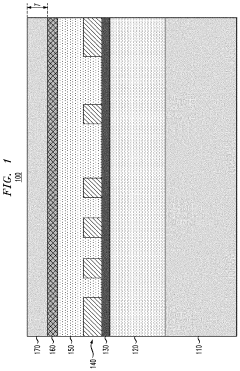
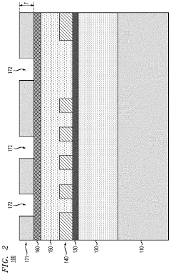
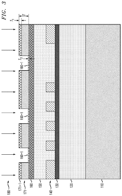
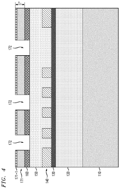
Extreme ultraviolet (EUV) lithography patterning methods utilizing EUV resist hardening
PatentInactiveUS10901317B2
Innovation
- Implementing a surface-hardened EUV resist mask with an etch-resistant layer formed by a neutral atom beam process that implants metallic or chemical species into the upper surface of the EUV resist mask to enhance etch resistance, allowing for patterning of sub-36 nm pitch features without significant mask thickness reduction.
Environmental Impact of EUV Resist Materials
The environmental impact of EUV resist materials represents a critical consideration in the semiconductor industry's sustainability efforts. These specialized photoresist compounds, essential for extreme ultraviolet lithography in next-generation logic nodes, contain various chemical components that pose significant environmental challenges throughout their lifecycle.
Metal-containing resists, particularly those incorporating tin, antimony, or other heavy metals, present substantial environmental concerns. These metals can persist in ecosystems, potentially bioaccumulating in food chains and causing long-term ecological damage if improperly managed. The manufacturing processes for these materials involve energy-intensive steps and hazardous precursors, contributing to their overall environmental footprint.
Waste management represents another major environmental challenge. During the lithography process, approximately 80-90% of applied resist becomes waste, requiring specialized treatment and disposal protocols. The semiconductor industry generates significant volumes of resist waste annually, with projections indicating this will increase as EUV adoption expands across more manufacturing facilities globally.
Water consumption and contamination also present environmental concerns. The development and rinsing processes for EUV resists require ultra-pure water in substantial quantities. Post-process wastewater contains resist residues, developers, and other chemicals that require advanced treatment before release. Some facilities report using up to 5,000 liters of water per wafer processed, highlighting the water intensity of these operations.
Regulatory frameworks addressing these environmental impacts continue to evolve globally. The European Union's REACH regulations and RoHS directives increasingly scrutinize semiconductor materials, while similar regulatory trends emerge in Asia and North America. These regulations are driving industry innovation toward greener alternatives and more sustainable manufacturing practices.
The semiconductor industry has responded with several sustainability initiatives. Leading companies have established resist recycling programs, recovering valuable components and reducing waste volumes by up to 30% in some cases. Research into bio-based resist platforms shows promise, with early prototypes demonstrating comparable performance while reducing environmental impact.
Advanced effluent treatment technologies specifically designed for semiconductor manufacturing are being deployed, capable of removing over 99% of resist compounds from wastewater. Additionally, industry consortia are developing standardized environmental impact assessment methodologies specifically for lithography materials to enable meaningful comparisons between different resist formulations.
Integration Challenges with Semiconductor Manufacturing Processes
The integration of EUV resist materials into next-generation logic node manufacturing processes presents significant challenges that require careful consideration and innovative solutions. The extreme ultraviolet lithography process operates at a wavelength of 13.5nm, which introduces unique integration complexities compared to traditional lithography methods.
Material compatibility issues arise when incorporating new EUV resist formulations with existing semiconductor manufacturing processes. These novel resists must maintain stability and performance while interacting with various process chemicals, including developers, rinse solutions, and etching agents. The chemical interactions between resist materials and underlying substrate layers can lead to pattern collapse, adhesion failures, or contamination issues that compromise device yield.
Process window optimization represents another critical integration challenge. EUV resists must deliver consistent performance across varying exposure doses, focus conditions, and process temperatures. The narrow process windows characteristic of advanced nodes leave minimal margin for error, requiring precise control of resist thickness, post-exposure bake conditions, and development parameters to achieve target critical dimensions.
Defectivity control becomes increasingly difficult as feature sizes shrink below 10nm. Particle contamination, resist residues, and pattern bridging defects can significantly impact device functionality. The integration of EUV resists demands enhanced filtration systems, cleanroom protocols, and defect inspection methodologies to identify and mitigate potential yield-limiting factors.
Line edge roughness (LER) and line width roughness (LWR) management presents persistent integration challenges. While inherent to the resist chemistry and exposure mechanisms, these roughness factors must be minimized through process optimization. Post-lithography treatments, including plasma smoothing techniques and specialized rinse processes, must be carefully integrated without compromising pattern fidelity.
Metrology integration poses additional challenges as traditional optical measurement techniques reach their resolution limits. New metrology approaches, including CD-SEM, scatterometry, and hybrid metrology solutions, must be calibrated specifically for EUV resist materials to provide accurate feedback for process control.
The transition from development to high-volume manufacturing requires addressing etch resistance properties of EUV resists. Pattern transfer fidelity depends on the resist's ability to withstand increasingly complex etch chemistries while maintaining critical dimensions. Integration of hardmask layers and etch process optimization becomes essential to compensate for potential limitations in resist etch selectivity.
Unlock deeper insights with Patsnap Eureka Quick Research — get a full tech report to explore trends and direct your research. Try now!
Generate Your Research Report Instantly with AI Agent
Supercharge your innovation with Patsnap Eureka AI Agent Platform!