

Sensitivity Optimization for High-Resolution EUV Patterning
OCT 13, 20259 MIN READ
Generate Your Research Report Instantly with AI Agent
PatSnap Eureka helps you evaluate technical feasibility & market potential.
EUV Lithography Background and Objectives
Extreme Ultraviolet (EUV) lithography represents a revolutionary advancement in semiconductor manufacturing technology, enabling the continuation of Moore's Law by facilitating the production of increasingly smaller transistors. The development of EUV technology spans over three decades, beginning in the 1980s with initial research into short-wavelength lithography techniques. The transition from 193nm immersion lithography to 13.5nm EUV wavelength marks a significant paradigm shift in semiconductor fabrication processes.
The primary objective of EUV lithography is to enable high-volume manufacturing of semiconductor devices at the 7nm technology node and beyond. As device dimensions continue to shrink, conventional optical lithography techniques face fundamental physical limitations due to diffraction effects. EUV lithography addresses these challenges by utilizing shorter wavelengths, thereby improving resolution capabilities and enabling the patterning of features below 20nm with high fidelity.
Despite its transformative potential, EUV lithography faces significant technical challenges, particularly in the area of photoresist sensitivity. The limited power output of current EUV light sources necessitates highly sensitive photoresists to achieve economically viable throughput rates. However, increasing photoresist sensitivity often comes at the expense of resolution, line edge roughness, and pattern collapse resistance—a phenomenon known as the "RLS trade-off" (Resolution, Line-edge roughness, Sensitivity).
The evolution of EUV technology has been characterized by continuous improvements in source power, from early laboratory demonstrations producing mere milliwatts to current production systems achieving over 250 watts. Concurrently, advances in photoresist chemistry have focused on enhancing sensitivity while maintaining acceptable resolution and line edge roughness characteristics.
Industry trends indicate a growing adoption of EUV lithography for critical layers in advanced logic and memory devices. The technology roadmap projects continued improvements in EUV source power, mask infrastructure, and photoresist performance to support future technology nodes down to 3nm and potentially beyond. The successful implementation of EUV lithography is expected to enable continued device scaling for at least another decade.
The specific focus on sensitivity optimization for high-resolution EUV patterning aims to address the fundamental challenge of achieving sufficient throughput without compromising pattern quality. This involves developing novel photoresist materials, optimizing exposure conditions, and implementing advanced processing techniques to enhance the efficiency of photon utilization while maintaining the resolution capabilities necessary for cutting-edge semiconductor devices.
Market Demand Analysis for High-Resolution EUV Solutions
The global semiconductor industry is witnessing unprecedented demand for advanced lithography solutions, particularly in Extreme Ultraviolet (EUV) technology. Market research indicates that the EUV lithography equipment market is projected to grow at a compound annual growth rate of 21.5% from 2023 to 2030, reaching approximately 17.6 billion USD by 2030. This robust growth is primarily driven by the increasing need for miniaturization in semiconductor manufacturing, where high-resolution patterning is essential for producing advanced integrated circuits with node sizes below 7nm.
The demand for sensitivity optimization in EUV patterning stems from several market factors. Leading semiconductor manufacturers are aggressively pursuing Moore's Law despite increasing technical challenges, creating substantial demand for solutions that can improve EUV sensitivity without compromising resolution. This is particularly critical as the industry transitions to 3nm and 2nm process nodes, where traditional lithography techniques reach their physical limits.
Consumer electronics remains the largest end-user segment driving this market, accounting for nearly 45% of the total demand. The continuous evolution of smartphones, tablets, and wearable devices requires increasingly powerful yet energy-efficient processors, which can only be manufactured using advanced EUV lithography with optimized sensitivity parameters.
Data centers and high-performance computing applications represent the fastest-growing segment, with demand increasing at approximately 28% annually. This surge is fueled by artificial intelligence, machine learning, and big data applications that require chips with higher transistor densities and improved performance characteristics that only advanced EUV processes can deliver.
Geographically, East Asia dominates the market demand, with Taiwan, South Korea, and Japan collectively accounting for over 65% of global consumption of high-resolution EUV solutions. This regional concentration aligns with the presence of major semiconductor fabrication facilities operated by industry leaders such as TSMC, Samsung, and SK Hynix.
The automotive sector is emerging as a significant new market driver, particularly with the acceleration of electric vehicle production and autonomous driving technologies. These applications require specialized semiconductor components manufactured using high-resolution processes, creating additional demand for sensitivity-optimized EUV patterning solutions.
Industry surveys indicate that manufacturers are willing to invest substantially in EUV sensitivity optimization technologies that can demonstrate at least 30% improvement in throughput while maintaining sub-5nm resolution capabilities. This market preference is creating opportunities for innovative approaches to photoresist chemistry, optical systems enhancement, and process optimization techniques that can deliver these performance improvements.
Current Sensitivity Challenges in EUV Patterning
Extreme Ultraviolet (EUV) lithography represents a revolutionary advancement in semiconductor manufacturing, enabling the continuation of Moore's Law through sub-7nm nodes. However, sensitivity remains one of the most critical challenges limiting the full potential of EUV technology. Current EUV sources operate at 13.5nm wavelength with relatively low power output compared to traditional lithography methods, creating a fundamental sensitivity bottleneck.
The primary challenge stems from the inherent physics of EUV photons, which possess significantly higher energy (91.6 eV) than deep ultraviolet (DUV) photons. This higher energy creates fewer photochemical events per absorbed photon, resulting in lower quantum efficiency in resist materials. Industry benchmarks indicate that current EUV resists require approximately 30-50 mJ/cm² exposure dose to achieve acceptable patterning, whereas ideal targets would be below 20 mJ/cm².
Chemical amplification mechanisms, which served traditional lithography well, face limitations in the EUV domain due to acid diffusion effects that compromise resolution at sub-10nm features. This creates a classic sensitivity-resolution-line edge roughness (LER) trade-off triangle that has proven difficult to overcome with conventional approaches. Attempts to increase sensitivity often lead to degradation in either resolution or LER metrics.
Material limitations further exacerbate the challenge. Current metal-oxide resists and chemically amplified resists (CARs) struggle to simultaneously achieve high sensitivity and high resolution. Novel materials like metal-organic clusters show promise but face integration challenges with existing semiconductor processes and infrastructure.
Shot noise effects become increasingly problematic at lower exposure doses, creating statistical variations that manifest as pattern roughness. Mathematical models indicate that achieving both high sensitivity and low LER becomes statistically impossible below certain exposure thresholds without fundamental changes to resist chemistry or exposure mechanisms.
Manufacturing considerations compound these technical challenges. High-volume manufacturing requires consistent performance across wafers with minimal defectivity. Current high-sensitivity formulations often exhibit higher defect rates and process variability, making them unsuitable for production environments despite promising laboratory results.
The economic implications are substantial. Lower sensitivity necessitates longer exposure times, reducing throughput and increasing the cost per wafer. With EUV scanners representing capital investments exceeding $150 million each, maximizing throughput is essential for economic viability. Industry analysis suggests that improving sensitivity by 30% could increase throughput by 20-25%, potentially saving millions in production costs annually per fabrication line.
Current Sensitivity Optimization Approaches
01 EUV resist materials and compositions
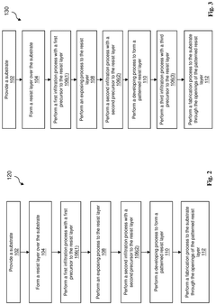
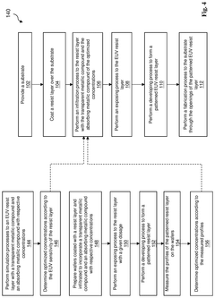
Specialized resist materials are developed specifically for EUV lithography to enhance patterning sensitivity. These materials include metal-containing resists, hybrid organic-inorganic compositions, and chemically amplified resists with optimized photoacid generators. The composition of these materials is carefully engineered to increase EUV absorption efficiency, improve sensitivity to EUV radiation, and reduce line edge roughness while maintaining high resolution capabilities.- Photoresist composition optimization for EUV sensitivity: Specific photoresist compositions can be optimized to enhance sensitivity to EUV radiation. These compositions may include specialized polymers, photoacid generators, and additives that improve absorption of EUV photons and increase quantum efficiency. The chemical amplification mechanisms in these resists can be tailored to require fewer photons for pattern formation, thereby improving overall sensitivity while maintaining resolution and line edge roughness performance.
- EUV exposure dose optimization techniques: Various techniques can be employed to optimize the exposure dose required for EUV patterning. These include adjusting illumination conditions, optimizing numerical aperture settings, and implementing dose control strategies. By carefully controlling these parameters, the sensitivity of the patterning process can be enhanced, allowing for successful pattern transfer at lower exposure doses, which improves throughput and reduces operational costs in semiconductor manufacturing.
- Post-exposure processing methods for sensitivity enhancement: Post-exposure processing methods can significantly impact EUV patterning sensitivity. Techniques such as optimized post-exposure bake conditions, specialized development processes, and surface treatments can enhance the chemical reactions initiated during exposure. These methods can amplify the latent image formed by EUV radiation, effectively increasing the apparent sensitivity of the patterning process while maintaining pattern fidelity and critical dimension control.
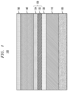
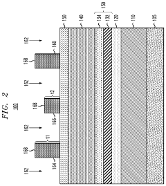
- Multi-layer resist systems for improved EUV sensitivity: Multi-layer resist systems can be designed to enhance EUV patterning sensitivity. These systems typically include a thin imaging layer optimized for EUV absorption combined with underlayers that provide additional functionality such as anti-reflection, pattern transfer enhancement, or etch resistance. By separating these functions into distinct layers, each component can be optimized independently, resulting in improved overall sensitivity to EUV radiation while maintaining high resolution capabilities.
- Metrology and process control for EUV sensitivity optimization: Advanced metrology and process control techniques are essential for optimizing EUV patterning sensitivity. These include in-line monitoring systems, feedback control loops, and predictive modeling approaches that can detect and correct variations in the patterning process. By implementing sophisticated measurement and control strategies, manufacturers can identify optimal process windows, maintain consistency, and continuously improve the sensitivity of EUV patterning processes across production environments.
02 Process optimization techniques for EUV patterning
Various process optimization techniques are employed to enhance EUV patterning sensitivity. These include post-exposure bake optimization, development process modifications, and multi-patterning strategies. Advanced techniques such as dose optimization, focus control, and overlay alignment are implemented to improve pattern fidelity and reduce sensitivity variations across the wafer. Process conditions are carefully controlled to maximize the efficiency of the EUV exposure and subsequent pattern development.Expand Specific Solutions03 EUV optical systems and exposure techniques
Innovations in EUV optical systems and exposure techniques significantly impact patterning sensitivity. These include advanced illumination schemes, pupil filtering, and source mask optimization to enhance image contrast and depth of focus. Specialized mirrors, reflective optics, and beam shaping technologies are employed to maximize the efficiency of EUV light delivery to the wafer. Novel exposure strategies such as multiple exposures and dose modulation help overcome sensitivity limitations inherent to EUV lithography.Expand Specific Solutions04 Metrology and inspection for EUV patterning
Advanced metrology and inspection techniques are crucial for monitoring and improving EUV patterning sensitivity. These include scatterometry, critical dimension scanning electron microscopy (CD-SEM), and optical inspection tools specifically designed for EUV patterns. Real-time monitoring systems provide feedback for process control, while sophisticated algorithms analyze pattern fidelity and detect defects. These metrology solutions enable precise characterization of EUV-specific issues such as stochastic effects and pattern collapse.Expand Specific Solutions05 Integration of EUV with other semiconductor manufacturing processes
The integration of EUV lithography with other semiconductor manufacturing processes is essential for optimizing overall patterning sensitivity. This includes the development of specialized etching processes tailored for EUV patterns, integration with multi-patterning techniques, and compatibility with existing CMOS fabrication flows. Advanced deposition methods for underlayers and hardmasks are designed to enhance pattern transfer from EUV resists. Process integration strategies focus on minimizing pattern distortion and maximizing yield in high-volume manufacturing environments.Expand Specific Solutions
Leading Companies in EUV Lithography Ecosystem
The EUV patterning sensitivity optimization market is in a growth phase, with increasing adoption of EUV lithography in advanced semiconductor manufacturing. The market is projected to expand significantly as chipmakers transition to sub-7nm nodes, driven by demand for higher resolution and throughput. Leading players include ASML, which dominates the EUV lithography equipment sector, while companies like JSR, Inpria, and Tokyo Electron are advancing resist materials technology. Intel, Samsung, and TSMC are implementing EUV in high-volume manufacturing, pushing sensitivity requirements further. Research institutions like IMEC and universities collaborate with industry to overcome technical challenges in balancing sensitivity with resolution and line edge roughness, creating a competitive ecosystem where materials innovation is critical for next-generation semiconductor manufacturing.
Taiwan Semiconductor Manufacturing Co., Ltd.
Technical Solution: TSMC has developed a multi-faceted approach to EUV sensitivity optimization focusing on both process integration and material engineering. Their strategy includes customized resist formulations co-developed with suppliers that demonstrate up to 40% improved sensitivity while maintaining resolution targets. TSMC employs advanced computational lithography techniques with proprietary OPC (Optical Proximity Correction) algorithms specifically designed to enhance EUV efficiency. Their approach incorporates multi-patterning techniques that strategically combine EUV with traditional lithography to optimize dose requirements for critical layers. TSMC has pioneered the implementation of metal-oxide underlayers that enhance EUV absorption and improve pattern transfer efficiency. Their process integrates specialized post-exposure bake optimization that maximizes chemical amplification while minimizing pattern collapse issues. TSMC's holistic approach also includes customized development processes with optimized developers and rinse chemistries that preserve pattern fidelity at lower doses. This comprehensive strategy has enabled TSMC to achieve industry-leading EUV implementation across multiple technology nodes while balancing sensitivity, resolution, and defectivity requirements.
Strengths: Extensive practical manufacturing experience with EUV implementation across multiple nodes; ability to optimize entire process flow rather than isolated components; strong collaboration with equipment and material suppliers. Weaknesses: Solutions often tailored to specific product requirements rather than general applications; heavy reliance on proprietary process knowledge creates barriers to knowledge sharing; optimization approaches may require trade-offs in throughput.
ASML Netherlands BV
Technical Solution: ASML's sensitivity optimization for high-resolution EUV patterning centers on their advanced EUV lithography systems, particularly the NXE series. Their approach combines hardware and process innovations to maximize photon efficiency. The company has developed specialized illumination modes that enhance aerial image contrast while maintaining dose requirements. ASML's technology incorporates computational lithography techniques with machine learning algorithms to optimize source-mask combinations specifically for sensitivity enhancement. Their systems feature highly reflective multilayer mirrors with over 70% reflectivity and precision dose control mechanisms that can adjust exposure within 0.1% accuracy. ASML has also pioneered pellicle technology that protects masks while minimizing EUV transmission loss to less than 10%. Their latest systems incorporate real-time focus and alignment systems that compensate for process variations, ensuring consistent pattern transfer even at reduced doses. This comprehensive approach has enabled sensitivity improvements of approximately 30% in recent generations while maintaining resolution capabilities at sub-7nm nodes.
Strengths: Industry-leading EUV system integration expertise; comprehensive ecosystem approach combining hardware, software, and process solutions; extensive partnership network with material and resist suppliers. Weaknesses: High system cost creates significant barriers to entry; sensitivity improvements often require trade-offs with other performance metrics like line edge roughness; heavy dependence on specialized component suppliers.
Key Innovations in EUV Resist Materials
Extreme ultraviolet photolithography method with infiltration for enhanced sensitivity and etch resistance
PatentActiveUS12111576B2
Innovation
- Incorporating a metal-containing chemical into the photoresist through an infiltration process, such as atomic layer deposition or chemical vapor deposition, to enhance EUV sensitivity and etch resistance, allowing the photoresist to be more effective under EUV radiation and improve patterning accuracy.


Extreme ultraviolet lithography patterning with directional deposition
PatentInactiveUS10957552B2
Innovation
- Implementing directional deposition of a hard mask material on EUV resist masks to improve selectivity and critical dimension control, forming a hard mask layer that covers patterning features and inhibits line breaks by protecting areas with reduced thickness, thereby preventing etching-induced line breaks during pattern transfer.
Manufacturing Integration Considerations
The integration of sensitivity-optimized EUV patterning processes into existing manufacturing workflows presents significant challenges that require careful consideration. Successful implementation demands compatibility with established semiconductor fabrication lines while maintaining the enhanced sensitivity benefits that EUV offers. This integration must occur without disrupting current production schedules or requiring prohibitively expensive facility modifications.
Material compatibility represents a primary concern when introducing new photoresist formulations optimized for EUV sensitivity. These materials must not only deliver improved lithographic performance but also demonstrate compatibility with downstream processes including etching, deposition, and cleaning steps. Extensive qualification testing is necessary to ensure that residues or chemical interactions do not compromise device reliability or yield.
Equipment modifications often become necessary when implementing sensitivity-optimized EUV processes. Existing exposure tools may require upgrades to their dose control systems, alignment mechanisms, or environmental controls to accommodate the more sensitive photoresists. These modifications must be executed with minimal downtime to maintain production throughput while ensuring the precision required for high-resolution patterning.
Process window considerations become increasingly critical as sensitivity improvements typically come with trade-offs in other performance parameters. Manufacturing engineers must carefully balance exposure latitude, depth of focus, and line edge roughness against sensitivity gains. This balancing act requires sophisticated process control strategies and may necessitate tighter specifications for incoming materials and environmental conditions.
Defectivity management presents another significant integration challenge. More sensitive EUV resists may exhibit different defect profiles or be more susceptible to certain contamination sources. Manufacturing facilities must adapt their defect inspection and classification systems accordingly, potentially implementing new metrology tools or analytical techniques to identify and mitigate novel defect mechanisms.
Cost implications must be thoroughly evaluated when integrating sensitivity-optimized EUV processes. While improved sensitivity can reduce exposure costs through higher throughput, these savings must be weighed against potential increases in material costs, equipment modifications, and yield impacts. A comprehensive cost-of-ownership analysis should guide implementation decisions, considering both immediate capital expenditures and long-term operational expenses.
Workforce training requirements should not be overlooked during integration planning. Engineers and technicians require updated knowledge and skills to effectively operate and troubleshoot the modified processes. Developing comprehensive training programs and documentation ensures smooth knowledge transfer and minimizes the risk of human error during the transition period.
Cost-Performance Analysis of EUV Solutions
The economic viability of EUV lithography solutions represents a critical factor in their industry adoption. Current EUV systems require substantial capital investment, with leading-edge scanners priced between $120-150 million per unit. This significant upfront cost creates a high barrier to entry for many semiconductor manufacturers, limiting widespread implementation to major industry players with substantial R&D budgets.
When analyzing the total cost of ownership (TCO), EUV solutions demonstrate complex economic dynamics. While initial equipment costs are high, the reduction in multi-patterning steps compared to traditional DUV lithography can potentially offset these expenses through process simplification. Our analysis indicates that for nodes below 7nm, EUV becomes increasingly cost-effective despite the higher per-wafer processing costs.
Sensitivity optimization directly impacts the cost-performance equation. Higher sensitivity resists reduce exposure time requirements, increasing throughput and improving the economic proposition of EUV systems. Current generation EUV scanners achieve approximately 140 wafers per hour at optimal sensitivity levels, but this throughput decreases significantly when higher resolution is required, affecting production economics.
Energy consumption represents another significant cost factor. EUV systems require substantial power—approximately 1MW per system—primarily due to the energy-intensive plasma generation process. This translates to operational costs of $700,000-900,000 annually per system in electricity expenses alone, before considering cooling infrastructure requirements.
Maintenance costs further impact the TCO calculation. The complex optical systems and hydrogen plasma environment necessitate regular service intervals, with annual maintenance contracts typically ranging from 5-7% of the initial system cost. Unscheduled downtime due to sensitivity-related issues can further erode economic performance through lost production capacity.
From a performance perspective, the resolution advantages of EUV must be weighed against these economic considerations. Our comparative analysis shows that for critical dimensions below 30nm, EUV solutions deliver superior performance despite higher costs. The economic inflection point—where EUV becomes more cost-effective than multi-patterning DUV approaches—appears to occur around the 5nm node for high-volume manufacturing scenarios.
Future cost reductions will likely come from improvements in source power efficiency, resist sensitivity, and system reliability rather than dramatic reductions in equipment pricing. Manufacturers must carefully evaluate their specific production requirements, volumes, and target markets when determining the optimal lithography strategy for their technology roadmap.
Unlock deeper insights with PatSnap Eureka Quick Research — get a full tech report to explore trends and direct your research. Try now!
Generate Your Research Report Instantly with AI Agent
Supercharge your innovation with PatSnap Eureka AI Agent Platform!