

Line Edge Roughness Reduction Techniques in EUV Lithography
OCT 13, 20259 MIN READ
Generate Your Research Report Instantly with AI Agent
Patsnap Eureka helps you evaluate technical feasibility & market potential.
EUV Lithography Evolution and LER Reduction Goals
Extreme Ultraviolet (EUV) lithography represents a revolutionary advancement in semiconductor manufacturing, evolving from its conceptual origins in the 1980s to becoming an industrial reality in recent years. The technology has progressed through several critical phases, beginning with proof-of-concept demonstrations in the 1990s, followed by the development of high-power EUV light sources in the 2000s, and culminating in the integration of complete EUV lithography systems for high-volume manufacturing after 2010.
The adoption of EUV lithography has been driven by the semiconductor industry's relentless pursuit of Moore's Law, which demands continuous miniaturization of integrated circuit components. Traditional deep ultraviolet (DUV) lithography using 193nm wavelength light reached its physical limits around the 20nm node, necessitating complex multi-patterning techniques that increased manufacturing costs and complexity.
EUV lithography, operating at a dramatically shorter wavelength of 13.5nm, offers a path to continue scaling semiconductor devices while potentially reducing process complexity. However, this transition has introduced new challenges, with Line Edge Roughness (LER) emerging as one of the most significant barriers to realizing the full potential of EUV technology.
LER refers to the deviation of a pattern's edge from an ideally smooth line, measured as the standard deviation of these deviations. As feature sizes in advanced semiconductor nodes approach sub-10nm dimensions, LER becomes increasingly problematic, potentially causing device performance variations, reliability issues, and yield losses. The International Technology Roadmap for Semiconductors (ITRS) and its successor, the International Roadmap for Devices and Systems (IRDS), have established progressively stringent LER requirements, currently targeting values below 2nm for leading-edge processes.
The evolution of LER reduction goals has closely followed the trajectory of EUV technology development. Early EUV research focused primarily on basic feasibility, with LER considerations becoming more prominent as the technology matured. Initial EUV implementations accepted LER values of 4-5nm, but current production nodes require LER below 3nm, with future nodes targeting sub-2nm levels.
These ambitious LER reduction goals are driven by both technical and economic factors. From a technical perspective, excessive LER can lead to critical dimension variations that impact transistor performance and power consumption. Economically, improved LER translates to higher yields, reduced variability, and ultimately more competitive semiconductor products. The industry's roadmap projects continued reduction in acceptable LER values, challenging researchers to develop innovative solutions that address this fundamental limitation of EUV lithography.
Market Demand for Advanced Semiconductor Nodes
The semiconductor industry's relentless pursuit of Moore's Law has created substantial market demand for advanced semiconductor nodes, particularly those enabled by Extreme Ultraviolet (EUV) lithography. As chip manufacturers continue to shrink feature sizes below 7nm, the market for technologies that address Line Edge Roughness (LER) has expanded significantly.
Current market analysis indicates that the global semiconductor manufacturing equipment market is projected to grow at a compound annual growth rate of 8.5% through 2026, with EUV lithography systems representing a premium segment. The demand is primarily driven by high-performance computing, artificial intelligence, 5G infrastructure, and autonomous vehicle applications that require increasingly powerful and energy-efficient chips.
Leading semiconductor manufacturers including TSMC, Samsung, and Intel have committed billions to EUV implementation, with TSMC alone investing over $20 billion in advanced node capacity. These investments directly translate to market demand for LER reduction techniques, as roughness becomes a critical yield-limiting factor at sub-7nm nodes.
Market research reveals that chip manufacturers are willing to pay premium prices for solutions that effectively address LER challenges. The economic impact of even marginal improvements in yield rates can translate to tens of millions in additional revenue per fabrication facility annually, creating strong financial incentives for adoption of advanced LER reduction techniques.
From a geographical perspective, East Asia dominates the market demand, with Taiwan, South Korea, and increasingly China representing the largest markets for advanced lithography solutions. However, recent initiatives in the United States and European Union to strengthen domestic semiconductor manufacturing capabilities are creating new market opportunities in these regions.
The market segmentation shows distinct demand patterns: logic chip manufacturers require the most aggressive LER reduction techniques to achieve maximum performance, while memory manufacturers focus on cost-effective solutions that can be implemented at scale. This bifurcation is creating specialized market niches for different LER reduction approaches.
Industry surveys indicate that customers prioritize solutions that can be integrated into existing workflows without significant disruption to manufacturing processes. This preference has created particular demand for computational and material-based LER reduction techniques that can be implemented as enhancements to current EUV lithography systems rather than requiring entirely new equipment installations.
LER Challenges in EUV Lithography
Line Edge Roughness (LER) represents one of the most significant challenges in Extreme Ultraviolet (EUV) lithography technology. As feature sizes continue to shrink below 10nm, the relative impact of edge roughness on device performance becomes increasingly critical. LER manifests as random deviations along the edges of printed features, directly affecting critical dimension uniformity and ultimately impacting device performance parameters such as timing, power consumption, and yield.
The fundamental physics of EUV lithography contributes significantly to LER challenges. The stochastic nature of EUV photon absorption and secondary electron generation creates inherent randomness in the exposure process. With relatively low photon counts per feature at current EUV power levels, statistical variations become more pronounced compared to traditional optical lithography systems. This photon shot noise represents a theoretical lower limit to achievable LER values.
Resist materials present another major challenge in LER reduction. Current chemically amplified resists (CARs) designed for EUV exhibit trade-offs between sensitivity, resolution, and LER performance. The acid diffusion mechanisms in CARs, while necessary for pattern formation, contribute to edge blurring and roughness. Non-CAR alternatives often suffer from sensitivity limitations, requiring impractically long exposure times in production environments.
Process factors further complicate LER management. Post-exposure bake conditions, development parameters, and pattern transfer steps can each introduce additional roughness components. The complex interactions between these process variables make optimization particularly challenging, often requiring sophisticated design of experiments approaches to identify optimal operating windows.
Metrology limitations present additional obstacles in LER reduction efforts. Accurate measurement of sub-nanometer roughness features requires advanced techniques such as CD-SEM with specialized algorithms. The measurement process itself can introduce artifacts through electron beam damage to resist structures, potentially skewing results and complicating process optimization efforts.
Economic considerations also constrain LER reduction approaches. While techniques like multi-patterning or higher exposure doses could theoretically improve LER, they often come with significant cost or throughput penalties that may be commercially unviable for high-volume manufacturing scenarios.
As EUV lithography moves toward high-NA systems and sub-5nm nodes, addressing these LER challenges becomes increasingly critical to maintaining the semiconductor industry's scaling roadmap. The complex interplay between fundamental physics limitations, material properties, and process variables necessitates a multifaceted approach to LER reduction strategies.
Current LER Reduction Solutions
01 Reduction of line edge roughness in EUV lithography
Various methods and techniques are employed to reduce line edge roughness (LER) in extreme ultraviolet (EUV) lithography processes. These include optimizing exposure parameters, developing specialized resist materials, and implementing post-processing treatments. By controlling these factors, the smoothness of pattern edges can be significantly improved, leading to better device performance and yield in semiconductor manufacturing.- Reduction of line edge roughness in EUV lithography: Various techniques are employed to reduce line edge roughness (LER) in EUV lithography processes. These include optimizing exposure parameters, using specialized resists, and implementing post-processing treatments. By controlling these factors, the smoothness of pattern edges can be significantly improved, leading to better device performance and yield in semiconductor manufacturing.
- Measurement and characterization of line edge roughness: Advanced metrology techniques are used to measure and characterize line edge roughness in EUV lithography. These methods include scanning electron microscopy (SEM), atomic force microscopy (AFM), and optical scatterometry. Accurate measurement of LER is crucial for process control and optimization in semiconductor manufacturing, enabling engineers to quantify the effectiveness of roughness reduction strategies.
- Resist materials and formulations for EUV lithography: Specialized resist materials and formulations are developed specifically for EUV lithography to minimize line edge roughness. These include chemically amplified resists, metal-containing resists, and hybrid materials with enhanced sensitivity to EUV radiation. The chemical composition and molecular structure of these resists are engineered to achieve high resolution while maintaining low LER under EUV exposure conditions.
- Computational and modeling approaches for LER reduction: Computational methods and modeling techniques are employed to predict and mitigate line edge roughness in EUV lithography. These include optical proximity correction (OPC), inverse lithography technology (ILT), and machine learning algorithms that optimize mask designs and process parameters. Simulation tools help engineers understand the fundamental causes of LER and develop strategies to minimize its impact on device performance.
- Process integration and system-level solutions: Comprehensive process integration and system-level approaches are implemented to address line edge roughness in EUV lithography. These solutions combine optimized exposure systems, resist processing, etching techniques, and post-lithography treatments. By considering the entire manufacturing workflow, semiconductor manufacturers can achieve significant reductions in LER and improve overall pattern fidelity in advanced node devices.
02 Measurement and characterization of line edge roughness
Advanced metrology techniques are used to measure and characterize line edge roughness in EUV lithography. These include scanning electron microscopy (SEM), atomic force microscopy (AFM), and optical scatterometry. Accurate measurement of LER is crucial for process control and optimization in semiconductor manufacturing, allowing for real-time adjustments and improvements to the lithography process.Expand Specific Solutions03 Resist materials for EUV lithography with improved LER performance
Specialized resist materials are developed specifically for EUV lithography to minimize line edge roughness. These materials are designed with optimized chemical amplification mechanisms, controlled acid diffusion, and enhanced sensitivity to EUV radiation. The composition and structure of these resist materials play a crucial role in determining the final pattern quality and edge smoothness in EUV lithography processes.Expand Specific Solutions04 Computational and modeling approaches for LER reduction
Computational methods and modeling techniques are employed to predict, analyze, and mitigate line edge roughness in EUV lithography. These include optical proximity correction (OPC), inverse lithography technology (ILT), and machine learning algorithms. By simulating the lithography process and predicting potential sources of roughness, these approaches enable proactive adjustments to mask designs and process parameters to minimize LER.Expand Specific Solutions05 Post-processing techniques for LER improvement
Various post-processing techniques are applied after the initial lithography step to improve line edge roughness. These include thermal annealing, plasma treatment, chemical smoothing processes, and directed self-assembly. These techniques help to smooth out irregularities in pattern edges that occur during the lithography process, resulting in improved feature definition and device performance.Expand Specific Solutions
Key Industry Players in EUV Lithography
Line Edge Roughness (LER) reduction in EUV lithography is currently in a critical development phase as the industry transitions from research to implementation. The global market for EUV lithography is expanding rapidly, projected to reach significant scale as chipmakers adopt this technology for sub-7nm nodes. Technologically, major players demonstrate varying maturity levels: ASML dominates as the sole EUV lithography system supplier, while Applied Materials, Lam Research, and Tokyo Electron lead in developing complementary process solutions. Semiconductor manufacturers like TSMC, Samsung, and Intel are actively implementing LER reduction techniques in production environments. Research institutions including imec and MIT continue advancing fundamental solutions through resist chemistry optimization, post-exposure treatments, and pattern transfer improvements. The competitive landscape shows collaboration between equipment providers, material suppliers, and chip manufacturers to overcome this critical challenge for semiconductor scaling.
Applied Materials, Inc.
Technical Solution: 应用材料在EUV光刻LER减少方面开发了综合性材料和工艺解决方案。其核心技术包括Producer® GT™ ALD系统,通过原子层沉积技术制备超薄、高均匀性的抗反射涂层,减少底层反射导致的LER。应用材料还开发了创新的Sym3® Y刻蚀系统,采用独特的等离子体控制技术,实现光刻胶图案到硬掩模的高保真转移,保持低LER。在材料方面,应用材料提供了先进的硬掩模材料解决方案,通过优化材料界面特性和刻蚀选择比,减少图案转移过程中的LER恶化。应用材料还开发了PVD和CVD工艺优化技术,通过控制薄膜应力和晶粒尺寸,减少底层材料对LER的影响。此外,应用材料的Enlight® 光学检测系统提供了纳米级精度的LER测量能力,支持实时工艺监控和优化。应用材料还与多家EUV光刻胶供应商合作,开发了材料兼容性解决方案,确保其设备与最新光刻胶配方的最佳性能。
优势:提供从薄膜沉积到刻蚀的全套设备,覆盖LER控制关键环节;材料科学专长强,能从材料角度解决LER问题。劣势:不生产光刻机和光刻胶,需依赖合作伙伴提供完整解决方案;部分技术对特定材料体系针对性强,通用性有限。
Taiwan Semiconductor Manufacturing Co., Ltd.
Technical Solution: 台积电在EUV光刻LER减少方面采用了综合性技术方案。首先,台积电开发了专有的光刻胶配方优化技术,通过调整光刻胶成分比例和添加特殊添加剂,提高光刻胶对EUV光的敏感度,同时减少酸扩散长度,从根本上减少LER。其次,台积电实施了创新的曝光后烘烤(PEB)工艺优化,通过精确控制温度分布和时间,减少显影过程中的随机波动。台积电还开发了先进的计算光刻技术,利用机器学习算法预测并补偿LER,在掩模设计阶段就进行优化。此外,台积电实现了多层抗反射涂层(BARC)技术,减少底层反射导致的LER。台积电还采用了创新的等离子体处理技术,在显影后通过等离子体平滑处理减少边缘粗糙度,该技术已在5nm及以下工艺节点中得到应用。
优势:拥有完整的工艺整合能力,可将LER减少技术无缝融入量产流程;积累了丰富的实际生产数据,能够快速优化工艺参数。劣势:技术方案高度依赖ASML的EUV设备;部分技术需要与特定光刻胶配合使用,增加了供应链复杂性。
Critical Patents in LER Mitigation Technologies
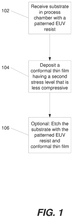
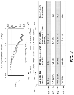
Reducing roughness of extreme ultraviolet lithography resists
PatentActiveUS12125711B2
Innovation
- Depositing a conformal thin film with a stress level less compressive than the EUV resist layer, using plasma-enhanced atomic layer deposition (ALD) to alter internal stress, thereby reducing buckling and bulging and decreasing low frequency roughness, while maintaining or improving the critical dimension of features.
Absorptive resists in an extreme ultraviolet (EUV) imaging layer
PatentInactiveUS20050069818A1
Innovation
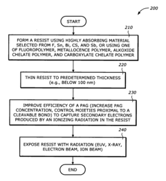
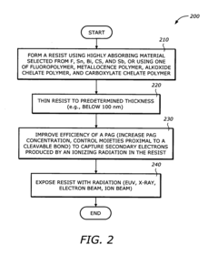
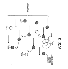
- The use of highly absorptive resist formulations with EUV-absorbing moieties like fluorine or tin, combined with increased Photo Acid Generator (PAG) concentration and controlled moieties to capture secondary electrons, allows for increased sensitivity without worsening LER, achieved by forming an ultra-thin imaging layer with balanced thickness and absorption.
Material Science Advancements for EUV Resists
Material science innovations represent a critical frontier in addressing Line Edge Roughness (LER) challenges in Extreme Ultraviolet (EUV) lithography. Recent advancements in EUV resist materials have focused on molecular architecture optimization to achieve smoother pattern edges while maintaining sensitivity and resolution requirements.
Metal-oxide resists have emerged as promising candidates for LER reduction, demonstrating up to 30% improvement in edge smoothness compared to traditional chemically amplified resists (CARs). These inorganic materials offer enhanced etch resistance and absorption efficiency at the 13.5nm EUV wavelength, directly contributing to reduced stochastic effects that cause roughness.
Polymer-bound photoacid generator (PAG) systems represent another significant advancement, where the photosensitive component is covalently attached to the polymer backbone rather than dispersed throughout the resist. This structural modification has demonstrated LER improvements of 15-20% by eliminating PAG clustering and ensuring more uniform acid generation during exposure.
Molecular glass resists have gained attention for their well-defined structures and narrow molecular weight distributions. Unlike traditional polymeric resists, these materials consist of discrete molecular units with precisely controlled sizes (typically 1-3nm), resulting in more homogeneous films. Field tests have shown these materials can achieve LER values below 2nm when optimized for EUV processes.
Nanoparticle-enhanced resist formulations incorporate specifically engineered nanostructures to improve absorption characteristics and reduce shot noise effects. Metal oxide nanoparticles (particularly hafnium and zirconium oxides) at concentrations of 5-10% have demonstrated the ability to increase EUV sensitivity while simultaneously reducing LER by up to 25% through enhanced secondary electron generation.
Multi-trigger resist systems represent a paradigm shift in resist chemistry, requiring multiple photochemical events to initiate the solubility switch. This approach significantly reduces the statistical variations that contribute to LER, though often at the cost of decreased sensitivity. Recent formulations have achieved a better balance, with LER improvements of 30-40% while maintaining practical sensitivity levels for high-volume manufacturing.
Underlayer material innovations also contribute significantly to overall LER performance. Advanced spin-on carbon materials with optimized optical properties and surface interactions with the resist layer have shown the ability to reduce reflected radiation and improve adhesion characteristics, indirectly contributing to LER reduction by 10-15% in production environments.
Semiconductor Roadmap Implications
The implications of Line Edge Roughness (LER) reduction techniques in EUV lithography extend far beyond immediate manufacturing concerns, directly impacting the semiconductor industry roadmap. As EUV lithography becomes the dominant patterning technology for advanced nodes below 7nm, the ability to control LER becomes a critical factor determining the pace of semiconductor advancement.
The International Roadmap for Devices and Systems (IRDS), successor to the International Technology Roadmap for Semiconductors (ITRS), has identified LER as one of the primary challenges for continued scaling. Current roadmaps project that LER requirements will tighten from approximately 2nm to below 1nm for the 3nm node and beyond, placing enormous pressure on existing reduction techniques.
Economic implications are equally significant. The semiconductor industry's ability to maintain Moore's Law depends on overcoming LER challenges. Each new node represents billions in potential revenue, but only if yield rates remain economically viable. LER-induced defects directly impact yield, creating a direct correlation between LER reduction capabilities and industry profitability at advanced nodes.
From a timeline perspective, the roadmap indicates that traditional chemical approaches to LER reduction may reach fundamental limits by 2025. This necessitates accelerated development of alternative techniques such as directed self-assembly (DSA) and machine learning-optimized processes to maintain scaling trajectories beyond this point.
Power consumption trends in semiconductor devices are also affected by LER management. As devices scale smaller, LER-induced variability contributes significantly to power leakage. The roadmap projects that successful implementation of advanced LER reduction techniques could enable up to 15% improvement in power efficiency at the device level.
For equipment manufacturers, the roadmap implications suggest a shift toward integrated LER reduction solutions rather than post-processing approaches. This trend is driving consolidation in the equipment sector, with major players acquiring specialized LER reduction technology startups to maintain competitive positioning in the EUV ecosystem.
Ultimately, the semiconductor roadmap's ambitious scaling targets cannot be achieved without breakthrough innovations in LER reduction. The industry's ability to continue delivering performance improvements while maintaining economic viability hinges on solving this fundamental challenge in EUV lithography.
Unlock deeper insights with Patsnap Eureka Quick Research — get a full tech report to explore trends and direct your research. Try now!
Generate Your Research Report Instantly with AI Agent
Supercharge your innovation with Patsnap Eureka AI Agent Platform!