Comparative Study of Metal-Oxide and Organic EUV Resists
OCT 13, 20259 MIN READ
Generate Your Research Report Instantly with AI Agent
Patsnap Eureka helps you evaluate technical feasibility & market potential.
EUV Resist Evolution and Objectives
Extreme Ultraviolet (EUV) lithography represents a revolutionary advancement in semiconductor manufacturing, enabling the continuation of Moore's Law by facilitating the production of increasingly smaller transistors. At the heart of this technology lies the EUV resist, a photosensitive material crucial for pattern transfer at the nanoscale. The evolution of EUV resists has been marked by significant technological milestones and persistent challenges that continue to drive innovation in this field.
Traditional photoresists, initially developed for 193nm lithography, proved inadequate for EUV applications due to fundamental differences in radiation interaction mechanisms. While 193nm lithography primarily relies on bond breaking through direct photon absorption, EUV lithography at 13.5nm wavelength involves complex secondary electron generation processes that necessitated entirely new resist chemistries and architectures.
The first generation of EUV resists emerged in the early 2000s, primarily based on chemically amplified resist (CAR) technology adapted from 193nm lithography. These organic-based materials offered familiar processing characteristics but struggled with sensitivity, resolution, and line edge roughness (LER) - the three critical parameters often referred to as the "triangle trade-off" in resist performance.
By the mid-2010s, the limitations of organic resists became increasingly apparent as semiconductor manufacturers pushed toward sub-10nm feature sizes. This prompted exploration of alternative materials, particularly metal-oxide based resists. These inorganic systems, incorporating elements such as hafnium, zirconium, and tin, demonstrated promising electron interaction properties and etch resistance characteristics that addressed some fundamental limitations of organic systems.
The objectives of current EUV resist development focus on simultaneously optimizing several critical parameters: sensitivity to reduce exposure time and increase throughput; resolution capability to enable smaller feature sizes; line edge roughness control to ensure device performance; and pattern collapse resistance to maintain structural integrity during development. Additionally, compatibility with existing manufacturing infrastructure remains essential for practical implementation.
Metal-oxide resists aim to achieve quantum leaps in performance by leveraging fundamentally different radiation interaction mechanisms compared to organic counterparts. Their development objectives include achieving sub-5nm resolution while maintaining practical sensitivity levels and addressing integration challenges such as defectivity and pattern transfer fidelity.
Meanwhile, organic resist development continues along evolutionary pathways, with objectives centered on incremental improvements through molecular engineering, novel amplification mechanisms, and advanced formulation strategies. Hybrid approaches combining elements of both technologies represent another promising direction, potentially offering the best attributes of each system.
The ultimate objective remains clear: developing resist materials capable of supporting semiconductor manufacturing at increasingly smaller nodes while maintaining economic viability and manufacturing reliability. This goal drives ongoing research across academic institutions, material suppliers, and semiconductor manufacturers worldwide.
Market Analysis for Advanced Lithography Materials
The Extreme Ultraviolet (EUV) lithography materials market is experiencing significant growth, driven by the semiconductor industry's push toward smaller node sizes and more complex chip architectures. Current market valuations place the global EUV resist materials sector at approximately $380 million in 2023, with projections indicating a compound annual growth rate of 15.8% through 2028, potentially reaching $790 million by that time.
Metal-oxide and organic EUV resists represent the two primary competing technologies in this space, with distinct market dynamics. Metal-oxide resists currently command about 35% of the market share, while traditional organic resists maintain dominance with roughly 60% share, with hybrid solutions accounting for the remainder.
Regional analysis reveals that East Asia continues to be the epicenter of demand, with South Korea, Taiwan, and Japan collectively accounting for over 70% of global consumption. This geographic concentration aligns with the presence of major semiconductor fabrication facilities in these regions. North America and Europe represent smaller but growing markets, particularly as these regions invest in semiconductor manufacturing sovereignty.
From an end-user perspective, the market is primarily driven by logic and memory chip manufacturers, with logic applications currently representing approximately 65% of EUV resist consumption. The increasing complexity of advanced logic nodes below 5nm has intensified demand for high-resolution, low-defect EUV resist materials.
Supply chain analysis indicates potential vulnerabilities, as production of high-purity precursors for both resist types remains concentrated among a limited number of specialty chemical suppliers. Recent geopolitical tensions and pandemic-related disruptions have highlighted these vulnerabilities, prompting increased investment in supply chain diversification.
Price sensitivity varies significantly between market segments. While cutting-edge semiconductor manufacturers prioritize performance over cost, the high price point of metal-oxide resists (typically 1.5-2x the cost of organic alternatives) remains a barrier to wider adoption in less demanding applications.
Market forecasts suggest that metal-oxide resists will gain market share over the next five years, potentially reaching 45-50% of the market by 2028, driven by their superior resolution capabilities and increasing process optimization. However, organic resists are expected to maintain significant market presence due to their established integration in manufacturing processes and ongoing innovations to improve sensitivity and line edge roughness performance.
Metal-Oxide vs Organic EUV Resists: Current Status
The current landscape of Extreme Ultraviolet (EUV) lithography resists presents a dichotomy between traditional organic materials and emerging metal-oxide alternatives. Organic resists, predominantly based on polymer or small molecule chemistries, have been the industry standard for decades. These materials typically utilize chemical amplification mechanisms where photoacids generated during exposure catalyze multiple chemical reactions, enhancing sensitivity. However, organic resists face significant challenges in the EUV regime, including limited absorption cross-sections at 13.5nm wavelength, pattern collapse at small feature sizes, and stochastic effects leading to line edge roughness.
Metal-oxide resists have emerged as promising alternatives, offering superior etch resistance and potentially better resolution capabilities. These inorganic materials, including hafnium, zirconium, and tin-based compounds, demonstrate higher EUV absorption coefficients due to the presence of heavy metal atoms. This enhanced absorption translates to improved sensitivity, a critical parameter for high-volume manufacturing where source power remains a limiting factor. Additionally, metal-oxide resists exhibit greater mechanical stability, mitigating pattern collapse issues that plague organic counterparts at sub-20nm feature sizes.
Current performance metrics reveal distinct trade-offs between these resist platforms. Organic resists generally offer better process integration compatibility with existing semiconductor manufacturing workflows and demonstrate superior line edge roughness characteristics in certain applications. However, they struggle to simultaneously meet the industry's stringent requirements for sensitivity, resolution, and line edge roughness—the so-called "triangle of death" in resist design.
Metal-oxide resists, while excelling in sensitivity and resolution aspects, face challenges in manufacturing scalability and process integration. The synthesis of these materials often involves complex sol-gel chemistry or nanoparticle formulations that can introduce variability in performance. Furthermore, their development processes differ significantly from established organic resist protocols, necessitating new equipment and process optimization.
Recent advancements have focused on hybrid approaches that combine the benefits of both platforms. These include metal-oxide nanoparticles dispersed in organic matrices or organometallic compounds that incorporate metal atoms into molecular structures. Such hybrid materials aim to leverage the high EUV absorption of metals while maintaining the processability of organic materials.
The geographical distribution of research efforts shows concentrated activities in East Asia, particularly Japan and South Korea, where major semiconductor manufacturers have established collaborations with material suppliers. North American research primarily stems from academic institutions and national laboratories, while European efforts are often coordinated through consortium approaches like IMEC.
Comparative Performance Analysis of EUV Resist Types
01 Metal-oxide based EUV resists
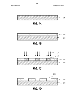
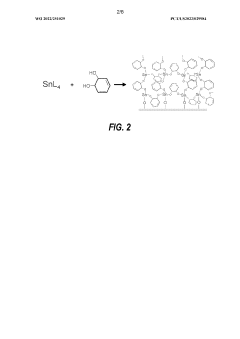
Metal-oxide based resists are emerging as promising materials for EUV lithography due to their high absorption cross-section for EUV radiation. These resists typically incorporate metal atoms such as hafnium, zirconium, or tin that strongly absorb EUV photons, leading to improved sensitivity. The metal-oxide components can be formulated as nanoparticles or molecular clusters embedded in a matrix, providing enhanced resolution and pattern fidelity compared to traditional organic resists. These materials often demonstrate reduced line edge roughness and better etch resistance, which are critical parameters for advanced semiconductor manufacturing.- Metal-oxide based EUV resists: Metal-oxide based resists are emerging as promising materials for EUV lithography due to their high absorption cross-section for EUV radiation. These resists typically incorporate metals such as hafnium, zirconium, or tin that strongly absorb EUV photons, leading to improved sensitivity. The metal-oxide nanoparticles are often dispersed in a matrix to form a hybrid resist system that combines the advantages of high EUV absorption with processability. These materials can achieve high resolution patterning with reduced line edge roughness compared to traditional organic resists.
- Organic EUV resist formulations: Organic EUV resists typically consist of polymer matrices with photoacid generators (PAGs) and various additives to enhance sensitivity and resolution. These resists rely on chemical amplification mechanisms where a single photon can trigger multiple chemical reactions through acid catalysis. Recent developments include the incorporation of fluorine-containing compounds to improve etch resistance and specialized quenchers to control acid diffusion. Organic resists offer advantages in terms of established processing methods and compatibility with existing semiconductor manufacturing infrastructure, though they generally have lower EUV absorption compared to metal-containing alternatives.
- Hybrid resist systems for EUV lithography: Hybrid resist systems combine organic matrices with inorganic components to leverage the benefits of both material types. These systems often incorporate metal clusters or nanoparticles into organic polymer frameworks to enhance EUV absorption while maintaining good processing characteristics. The organic components provide film-forming properties and established development processes, while the inorganic elements boost sensitivity to EUV radiation. These hybrid approaches aim to overcome the limitations of purely organic or purely inorganic systems, offering a balance of sensitivity, resolution, and manufacturing compatibility.
- EUV resist additives and performance enhancers: Various additives are incorporated into EUV resists to enhance their performance characteristics. These include sensitizers that improve photon absorption, quenchers that control acid diffusion to enhance resolution, and surfactants that improve coating uniformity. Other additives focus on reducing line edge roughness, improving adhesion to substrates, or enhancing etch resistance. Recent innovations include compounds that can reduce out-of-band radiation effects and materials that minimize pattern collapse during development. The careful selection and optimization of these additives is crucial for achieving the high resolution and sensitivity required for advanced semiconductor manufacturing.
- Processing techniques for EUV resists: Specialized processing techniques have been developed to optimize the performance of EUV resists. These include post-exposure bake optimization to control acid diffusion in chemical amplification resists, development processes tailored to specific resist chemistries, and thin film coating methods to ensure uniform resist layers. Advanced techniques such as track processing parameters, multi-patterning approaches, and specialized rinse solutions help to minimize pattern collapse and improve feature fidelity. Additionally, novel development methods including supercritical CO2 development and metal-specific developers have been introduced for metal-oxide resists to achieve higher resolution patterning.
02 Organic EUV resist formulations
Organic EUV resists continue to be developed with improved sensitivity and resolution capabilities. These formulations typically consist of polymer matrices with acid-labile protecting groups, photoacid generators, and various additives to enhance performance. Recent innovations focus on reducing outgassing during exposure, improving line edge roughness, and enhancing sensitivity to meet the demands of high-volume manufacturing. Chemical amplification mechanisms are often employed to increase sensitivity, while specialized polymer architectures help achieve the resolution requirements for advanced node semiconductor fabrication.Expand Specific Solutions03 Hybrid organic-inorganic EUV resist systems
Hybrid resist systems combine the advantages of both organic and inorganic materials to achieve optimal EUV lithography performance. These formulations typically incorporate metal-containing compounds into organic polymer matrices, creating materials with enhanced EUV absorption and improved pattern transfer characteristics. The organic components provide processability and film-forming properties, while the inorganic elements contribute to sensitivity and etch resistance. These hybrid approaches often demonstrate better resolution-sensitivity-line edge roughness trade-offs compared to purely organic or inorganic systems.Expand Specific Solutions04 EUV resist additives and performance enhancers
Various additives are incorporated into EUV resists to enhance specific performance characteristics. These include quenchers to control acid diffusion, sensitizers to improve quantum efficiency, surfactants for better coating properties, and plasticizers to modify mechanical properties. Recent developments focus on additives that can reduce pattern collapse, minimize line edge roughness, and improve adhesion to substrates. Specialized molecules that can capture secondary electrons or mitigate outgassing during exposure are also being developed to address EUV-specific challenges in high-volume manufacturing environments.Expand Specific Solutions05 Processing techniques for EUV resists
Advanced processing techniques are essential for optimizing the performance of EUV resists. These include specialized post-exposure bake conditions, development processes, and pattern transfer methods tailored to the unique characteristics of EUV lithography. Techniques such as thin film optimization, multi-layer resist approaches, and specialized underlayers help improve resolution and pattern fidelity. Recent innovations focus on reducing pattern collapse through controlled drying techniques, optimizing development conditions to enhance contrast, and implementing specialized rinse processes to improve line edge roughness and critical dimension uniformity.Expand Specific Solutions
Leading Manufacturers and Research Institutions
The EUV resist technology landscape is evolving rapidly, with competition between metal-oxide and organic approaches intensifying as the semiconductor industry transitions to advanced nodes. Currently in the growth phase, this market is expanding significantly due to increasing demand for high-resolution lithography in sub-7nm processes. While organic resists dominated historically, metal-oxide alternatives from companies like ASML, Tokyo Electron, and Samsung SDI are gaining traction due to superior resolution and sensitivity characteristics. Taiwan Semiconductor Manufacturing Co. and Intel are driving adoption as key end-users, while materials specialists including Shin-Etsu Chemical, Sumitomo Chemical, and Irresistible Materials are advancing both technologies through significant R&D investments. The ecosystem includes equipment providers like Applied Materials and Lam Research supporting integration challenges.
Taiwan Semiconductor Manufacturing Co., Ltd.
Technical Solution: TSMC has developed advanced metal-oxide EUV resist technologies optimized for high-volume manufacturing at 5nm and below nodes. Their metal-oxide resist platform incorporates hafnium-based inorganic materials with tailored ligand chemistry to achieve high sensitivity (15-20 mJ/cm²) while maintaining resolution below 13nm half-pitch [1]. TSMC's approach includes proprietary development processes that reduce pattern collapse through controlled dissolution kinetics. They've implemented multi-layer resist stacks with specialized underlayers that enhance pattern transfer fidelity and etch resistance. Recent innovations include metal-oxide nanoparticle formulations with surface modifications to improve dispersion stability and shelf-life beyond 6 months [3]. TSMC has also developed specialized post-exposure bake processes that optimize the acid diffusion in hybrid metal-oxide systems, resulting in improved line edge roughness (LER) values of approximately 2.2nm [5].
Strengths: Superior etch resistance compared to organic resists, enabling higher aspect ratio features; excellent thermal stability allowing for more aggressive post-processing; inherently lower outgassing during exposure. Weaknesses: Higher material costs; more complex processing requirements; potential for metal contamination in process tools requiring specialized cleaning protocols.
ASML Netherlands BV
Technical Solution: ASML has developed a comprehensive EUV resist evaluation platform that enables comparative analysis of both metal-oxide and organic resist technologies. Their approach integrates specialized metrology tools with their EUV lithography systems to provide real-time performance data. ASML's platform includes proprietary computational models that predict resist behavior under various exposure conditions, allowing for rapid optimization of process parameters [2]. Their metal-oxide resist characterization methodology incorporates stochastic effects modeling that accounts for photon shot noise and material quantum yield. For organic resists, ASML has developed specialized outgassing measurement techniques that quantify contamination risks to optical components. Their comparative framework evaluates resists across multiple metrics including sensitivity (dose-to-size), resolution, line edge roughness, and pattern collapse margin [4]. ASML's holistic approach also considers integration aspects such as etch selectivity, defectivity, and compatibility with existing semiconductor manufacturing infrastructure.
Strengths: Comprehensive evaluation methodology that considers both lithographic performance and integration requirements; ability to rapidly screen multiple resist formulations; deep understanding of EUV-specific challenges like stochastic effects. Weaknesses: As an equipment supplier rather than a materials developer, relies on partnerships for actual resist formulation; evaluation platform may favor certain resist characteristics based on tool architecture.
Key Patents and Scientific Breakthroughs
Methods for Extreme Ultraviolet (EUV) Resist Patterning Development
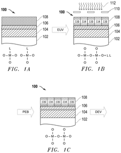
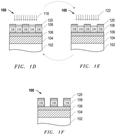
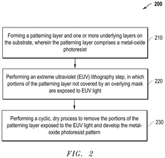
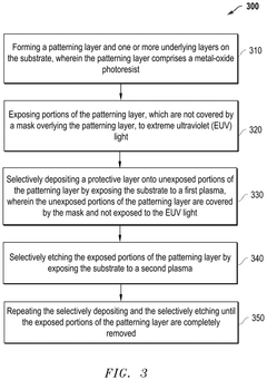
PatentPendingUS20250076771A1
Innovation
- A novel process flow and method for patterning metal-oxide photoresists using EUV or lower wavelength light, which involves forming a patterning layer, exposing it to EUV light to separate organic ligands from metal-oxide structures, followed by a bake process and a cyclic dry plasma process to develop the pattern.
Metalorganic films for extreme ultraviolet patterning
PatentWO2022251029A1
Innovation
- The development of metalorganic films containing tin, which are vapor-deposited on semiconductor substrates and patterned using EUV irradiation, offering higher EUV absorbance and etch resistance, and a more uniform chemical composition compared to conventional polymer-based chemically amplified resists, thereby mitigating secondary electron effects.
Environmental Impact and Sustainability Considerations
The environmental impact of EUV lithography materials represents a critical consideration in semiconductor manufacturing sustainability. Metal-oxide and organic EUV resists demonstrate significantly different ecological footprints throughout their lifecycle. Metal-oxide resists, particularly those containing heavy metals such as hafnium, zirconium, and tin, pose substantial environmental concerns related to mining, processing, and disposal. The extraction processes for these metals often involve energy-intensive operations and can result in habitat destruction, water pollution, and soil contamination in mining regions.
In contrast, organic EUV resists typically utilize carbon-based polymers and photoacid generators that generally require less environmentally damaging extraction processes. However, organic resists frequently incorporate fluorinated compounds and antimony-based components that present their own environmental challenges, including persistence in ecosystems and potential toxicity to aquatic organisms.
Manufacturing processes for both resist types consume substantial energy and chemicals. Metal-oxide resists often require higher temperature processing and specialized deposition techniques, resulting in greater energy consumption. Organic resists typically involve complex synthesis routes with multiple chemical reactions and purification steps that generate significant waste streams requiring specialized treatment.
Waste management represents another crucial environmental consideration. Metal-oxide resist waste contains heavy metal residues that may require classification as hazardous materials, necessitating specialized disposal protocols and increasing environmental liability. Organic resist waste, while potentially less toxic in some aspects, often contains persistent organic pollutants that resist conventional wastewater treatment methods.
Recent sustainability initiatives in the semiconductor industry have begun addressing these concerns through several approaches. Closed-loop recycling systems for metal-oxide materials are being developed to recover valuable metals from manufacturing waste. For organic resists, research focuses on biodegradable alternatives and reduced use of environmentally persistent compounds. Additionally, process optimization efforts aim to minimize chemical usage and waste generation for both resist types.
Regulatory frameworks worldwide are increasingly imposing stricter controls on hazardous materials in electronics manufacturing. The European Union's Restriction of Hazardous Substances (RoHS) directive and similar regulations in other regions may impact future resist formulations, potentially accelerating the transition toward more environmentally benign alternatives. This regulatory landscape creates both challenges and opportunities for resist manufacturers to develop more sustainable solutions while maintaining the high performance required for advanced semiconductor nodes.
Integration Challenges with Existing Semiconductor Processes
The integration of EUV resist technologies into existing semiconductor manufacturing processes presents significant challenges that require careful consideration. Metal-oxide and organic EUV resists each introduce unique integration hurdles that impact the overall semiconductor fabrication workflow.
Metal-oxide resists, while offering superior resolution and etch resistance, present considerable integration difficulties with conventional semiconductor processes. Their inorganic nature creates compatibility issues with standard development and stripping chemicals optimized for organic materials. The metal content in these resists can potentially contaminate process equipment and subsequent layers, necessitating specialized handling protocols and dedicated tools to prevent cross-contamination.
Organic EUV resists align more closely with traditional photoresist processing, allowing for smoother integration with existing lithography equipment and chemical processes. However, they introduce different challenges related to their limited etch resistance and pattern collapse at small feature sizes, requiring process modifications to maintain yield and reliability.
Both resist types demand significant adjustments to post-exposure processing steps. Metal-oxide resists typically require specialized developers and more aggressive stripping processes, while organic resists may need modified development conditions to optimize pattern fidelity. These differences necessitate careful process qualification and potentially separate processing lines, increasing manufacturing complexity.
The metrology and inspection systems must also adapt to accommodate the different optical and physical properties of these resist materials. Metal-oxide resists often exhibit different reflectivity and scattering behaviors compared to organic counterparts, requiring recalibration of optical inspection tools and potentially new metrology approaches.
From a supply chain perspective, the introduction of metal-oxide resists requires establishing new material sourcing channels and quality control protocols. The metals used in these formulations may be subject to different regulatory requirements and supply constraints compared to the organic compounds used in traditional resists.
The waste treatment processes must also be reconsidered, particularly for metal-oxide resists. The metal components may require specialized disposal methods to comply with environmental regulations, adding complexity to fab operations and potentially increasing operational costs.
Ultimately, the successful integration of either resist technology requires comprehensive evaluation of the entire process flow, from material handling through final inspection, with careful attention to compatibility with existing equipment, processes, and environmental systems.
Unlock deeper insights with Patsnap Eureka Quick Research — get a full tech report to explore trends and direct your research. Try now!
Generate Your Research Report Instantly with AI Agent
Supercharge your innovation with Patsnap Eureka AI Agent Platform!