

Comparative Study of Coating Techniques for Neuromorphic Chips
OCT 9, 202510 MIN READ
Generate Your Research Report Instantly with AI Agent
Patsnap Eureka helps you evaluate technical feasibility & market potential.
Neuromorphic Coating Evolution and Objectives
Neuromorphic computing, inspired by the human brain's neural architecture, has evolved significantly since its conceptual inception in the late 1980s by Carver Mead. The field has progressed from basic analog VLSI implementations to today's sophisticated neuromorphic chips that emulate neural networks with unprecedented efficiency. This evolution has been marked by continuous improvements in materials science, particularly in coating technologies that enhance chip performance, durability, and functionality.
The development trajectory of neuromorphic coating techniques can be traced through several distinct phases. Initially, conventional semiconductor coatings were adapted for neuromorphic applications, providing basic protection and conductivity. The second phase saw the introduction of specialized coatings designed to enhance specific neuromorphic functions, such as mimicking synaptic plasticity. Currently, we are witnessing the emergence of advanced multi-functional coatings that simultaneously address multiple requirements of neuromorphic systems.
Material innovation has been central to this evolution. Traditional silicon-based coatings have given way to novel materials including metal oxides, organic polymers, and more recently, two-dimensional materials like graphene and transition metal dichalcogenides. These advanced materials offer superior electrical properties, enhanced thermal management, and improved resistance to environmental factors that can degrade chip performance.
The primary objective of modern neuromorphic coating research is to develop techniques that enable chips to more accurately mimic the brain's neural architecture while maintaining energy efficiency. This includes creating coatings that facilitate spike-timing-dependent plasticity (STDP), a fundamental mechanism for learning in biological systems. Additionally, researchers aim to develop coatings that can withstand the unique operational conditions of neuromorphic systems, including variable voltage spikes and complex thermal patterns.
Another critical goal is scalability. As neuromorphic computing moves from research laboratories to commercial applications, coating techniques must be adaptable to mass production while maintaining precision and quality. This necessitates the development of coating methods that are both cost-effective and compatible with existing semiconductor manufacturing infrastructure.
Looking forward, the field is trending toward biomimetic coatings that not only protect and enhance neuromorphic chips but also actively contribute to their computational capabilities. These include self-healing coatings that can repair minor damage, adaptive coatings that modify their properties based on operational conditions, and even biohybrid coatings that incorporate biological materials to bridge the gap between silicon-based computing and biological neural networks.
The ultimate objective remains clear: to develop coating technologies that enable neuromorphic chips to achieve brain-like efficiency, adaptability, and cognitive capabilities while operating within the constraints of electronic systems.
Market Analysis for Neuromorphic Computing Solutions
The neuromorphic computing market is experiencing significant growth, driven by increasing demand for AI applications that require efficient processing of neural network workloads. Current market valuations place the global neuromorphic computing sector at approximately 3.2 billion USD in 2023, with projections indicating a compound annual growth rate of 24.7% through 2030. This remarkable expansion reflects the technology's potential to revolutionize computing paradigms across multiple industries.
Market segmentation reveals diverse application areas for neuromorphic chips, with particularly strong demand in autonomous vehicles, robotics, healthcare diagnostics, and edge computing devices. The automotive sector represents the largest market share at 28%, followed by consumer electronics at 22% and healthcare at 17%. This distribution highlights the versatility of neuromorphic solutions in addressing complex computational challenges across industries.
Customer needs analysis indicates that power efficiency remains the primary driver for neuromorphic adoption, with organizations seeking solutions that deliver AI capabilities while minimizing energy consumption. Survey data from enterprise customers shows that 76% prioritize energy efficiency, 64% value real-time processing capabilities, and 58% emphasize reduced form factors. These requirements directly influence coating techniques for neuromorphic chips, as thermal management and protection from environmental factors become critical considerations.
Regional market analysis reveals significant geographical variations in adoption patterns. North America currently leads with 42% market share, bolstered by substantial investments in neuromorphic research and strong presence of technology companies. Asia-Pacific follows at 35% and is projected to demonstrate the fastest growth rate at 29.3% annually, driven primarily by manufacturing capabilities and increasing AI adoption in China, South Korea, and Japan. Europe accounts for 19% of the market, with particular strength in research-oriented applications.
Competitive landscape assessment identifies three distinct market segments for neuromorphic computing solutions: high-performance computing, embedded systems, and specialized research applications. Each segment presents unique requirements for chip coating technologies, with high-performance computing prioritizing thermal management, embedded systems focusing on durability and longevity, and research applications emphasizing flexibility and customization options.
Market barriers include high initial costs, with neuromorphic solutions typically commanding a 30-40% premium over traditional computing architectures. Additionally, integration challenges with existing systems and limited developer familiarity with neuromorphic programming paradigms constrain broader adoption. These factors directly impact coating technology decisions, as manufacturers seek to balance performance enhancement with cost-effective production methods.
Global Landscape and Technical Barriers in Chip Coating
The global landscape of coating technologies for neuromorphic chips reveals significant disparities in technological advancement and adoption across different regions. North America, particularly the United States, maintains leadership in advanced coating techniques, with major research institutions like MIT, Stanford, and industrial giants such as IBM and Intel driving innovation. These entities have established robust intellectual property portfolios in atomic layer deposition (ALD) and plasma-enhanced chemical vapor deposition (PECVD) specifically optimized for neuromorphic architectures.
Europe follows closely, with strong research clusters in Germany, France, and the Netherlands. European research emphasizes environmentally sustainable coating methods and precision engineering, with organizations like Fraunhofer Society and IMEC developing specialized coating solutions that address the unique requirements of bio-inspired computing systems. Their focus on high-precision, low-temperature coating processes has yielded significant advancements in reliability and performance.
The Asia-Pacific region, particularly Japan, South Korea, and Taiwan, demonstrates exceptional capabilities in mass production and scaling of coating technologies. Companies like TSMC and Samsung have developed proprietary coating methods that enable high-volume manufacturing of neuromorphic chips with consistent quality. China is rapidly closing technological gaps through substantial investments in research infrastructure and talent acquisition, particularly in novel materials for neuromorphic applications.
Despite global progress, several critical technical barriers persist in neuromorphic chip coating. The most significant challenge involves achieving uniform coatings at nanoscale dimensions while maintaining precise control over thickness and composition. This becomes increasingly difficult as neuromorphic architectures incorporate more complex 3D structures and higher aspect ratios, creating issues with step coverage and material penetration into deep trenches.
Another major obstacle is the thermal budget constraint. Many neuromorphic designs incorporate temperature-sensitive materials that simulate synaptic functions, necessitating low-temperature coating processes that don't compromise these delicate structures. This limitation restricts the available coating techniques and often forces trade-offs between coating quality and preserving underlying functionality.
Interface engineering presents additional challenges, as the coating-substrate interface critically influences electrical characteristics and long-term reliability. Controlling interfacial reactions and minimizing defect formation during deposition processes remains technically demanding, particularly for materials combinations unique to neuromorphic systems.
Emerging barriers include developing coating techniques compatible with novel neuromorphic materials such as phase-change memory elements, memristive oxides, and spintronic components. These materials often require specialized coating environments and precise stoichiometry control that exceed the capabilities of conventional equipment.
Current Coating Methodologies for Neuromorphic Architectures
01 Atomic Layer Deposition for Neuromorphic Devices
Atomic Layer Deposition (ALD) is a precision coating technique used for neuromorphic chips to create ultra-thin, uniform layers of materials with atomic-level control. This technique allows for the deposition of high-quality dielectric layers, resistive switching materials, and barrier films essential for memristive devices. The precise thickness control enables the fabrication of nanoscale structures with consistent electrical properties, which is crucial for reliable synaptic behavior in neuromorphic computing applications.- Atomic Layer Deposition for Neuromorphic Devices: Atomic Layer Deposition (ALD) is a precision coating technique used for neuromorphic chips to create ultra-thin, uniform films with atomic-level control. This method enables the deposition of high-quality dielectric layers, resistive switching materials, and barrier films essential for memristive devices. The technique allows for conformal coating even on complex 3D structures, which is crucial for advanced neuromorphic architectures with high aspect ratio features. ALD processes can be optimized for temperature-sensitive substrates while maintaining excellent film quality and interface properties.
- Resistive Switching Material Coatings: Specialized coating techniques for resistive switching materials are fundamental to neuromorphic chip functionality. These coatings typically involve metal oxides like HfO2, TiO2, or Ta2O5 that can be precisely deposited to form the active layer in memristive devices. The composition, thickness, and defect concentration in these films directly influence synaptic behavior, including potentiation, depression, and retention characteristics. Advanced deposition methods enable the creation of multi-layer stacks with engineered interfaces to enhance switching reliability and endurance while reducing variability across devices.
- Encapsulation and Passivation Techniques: Protective coating methods for neuromorphic chips involve encapsulation and passivation layers that shield sensitive components from environmental factors. These techniques utilize materials such as silicon nitride, alumina, or specialized polymers to prevent moisture ingress and ion migration that could degrade device performance. The encapsulation process must maintain low thermal budgets to avoid damaging temperature-sensitive neuromorphic elements while providing hermetic sealing. Advanced passivation approaches can also incorporate getter materials to absorb residual gases or contaminants within the package.
- 2D Material Coating for Neural Interfaces: Two-dimensional materials like graphene, MoS2, and hexagonal boron nitride offer unique advantages when coated onto neuromorphic chips. These atomically thin layers can be deposited through chemical vapor deposition or solution-based methods to create flexible neural interfaces with exceptional electrical properties. The 2D material coatings enable high-density integration of synaptic elements while maintaining low power consumption. These materials also demonstrate excellent biocompatibility for neuromorphic systems designed to interface with biological neurons, allowing for enhanced signal transduction between electronic and biological systems.
- Phase Change Material Deposition: Phase change materials (PCMs) require specialized coating techniques for integration into neuromorphic computing architectures. These materials, typically chalcogenide alloys like Ge2Sb2Te5, can be deposited using sputtering, thermal evaporation, or pulsed laser deposition to achieve precise stoichiometry and crystallization properties. The deposition parameters critically influence the switching speed, power consumption, and multi-level storage capabilities of PCM-based synaptic elements. Advanced techniques include confined cell structures and interface engineering to reduce drift and improve retention characteristics essential for long-term neuromorphic operation.
02 Spin Coating Methods for Neuromorphic Materials
Spin coating is widely employed for applying uniform thin films of organic and solution-processable materials on neuromorphic chips. This technique involves depositing a solution onto a substrate and rotating it at high speed to spread the material evenly through centrifugal force. It's particularly valuable for coating polymer-based memristive materials, organic semiconductors, and phase-change materials that form the functional layers in neuromorphic devices. The method offers advantages in terms of simplicity, cost-effectiveness, and compatibility with various material systems.Expand Specific Solutions03 Physical Vapor Deposition Techniques for Neural Networks
Physical Vapor Deposition (PVD) techniques, including sputtering and thermal evaporation, are essential for coating neuromorphic chips with metallic electrodes, resistive switching layers, and other functional materials. These methods involve converting solid materials into vapor phase under vacuum conditions and then condensing them onto the substrate. PVD enables precise control over film composition, thickness, and microstructure, which directly influences the performance characteristics of neuromorphic devices such as switching speed, endurance, and power consumption.Expand Specific Solutions04 Encapsulation and Protective Coatings for Neuromorphic Systems
Protective encapsulation coatings are critical for ensuring the long-term reliability and stability of neuromorphic chips. These coatings shield sensitive neuromorphic elements from environmental factors such as moisture, oxygen, and contaminants that could degrade performance. Advanced encapsulation techniques include conformal barrier films, hermetic sealing methods, and composite protective layers that maintain the electrical properties of the underlying devices while providing robust environmental protection. These approaches extend device lifetime and maintain consistent neuromorphic behavior under various operating conditions.Expand Specific Solutions05 Solution-Based Coating Methods for Scalable Neuromorphic Fabrication
Solution-based coating techniques offer scalable approaches for fabricating neuromorphic devices, including dip coating, spray coating, and inkjet printing. These methods enable the deposition of various functional materials including metal oxides, nanoparticles, and organic compounds that serve as the active elements in neuromorphic architectures. Solution processing allows for large-area fabrication, pattern formation, and multi-layer structures at lower costs compared to vacuum-based methods. The versatility of solution processing facilitates the integration of diverse materials with complementary properties for enhanced neuromorphic functionality.Expand Specific Solutions
Industry Leaders and Competitive Dynamics in Neuromorphic Hardware
The neuromorphic chip coating techniques market is in an early growth phase, characterized by significant research activity but limited commercial deployment. The global market size is estimated to be relatively modest but growing rapidly as neuromorphic computing gains traction in AI applications. From a technical maturity perspective, the field shows varying degrees of advancement among key players. IBM and Samsung lead with established semiconductor coating expertise, while specialized neuromorphic players like Syntiant and Beijing Lingxi Technology are developing innovative coating solutions specifically for brain-inspired architectures. Academic institutions including Tsinghua University, Zhejiang University, and USC contribute fundamental research, while CEA and SK Hynix focus on materials science advancements. TDK and Dexerials bring specialized coating materials expertise, creating a competitive landscape balanced between established semiconductor giants and emerging neuromorphic specialists.
International Business Machines Corp.
Technical Solution: IBM has pioneered advanced coating techniques for neuromorphic chips through their TrueNorth and subsequent neuromorphic architectures. Their approach utilizes precision atomic layer deposition (ALD) for creating uniform, defect-free dielectric layers critical for reliable neuromorphic operation. IBM's coating methodology incorporates specialized phase-change materials (PCMs) that enable efficient synaptic weight storage with nanometer-scale precision. Their proprietary multi-layer coating process allows for the integration of both volatile and non-volatile memory elements within the same neuromorphic architecture, enhancing the chip's ability to mimic biological neural networks. IBM has also developed specialized passivation techniques that significantly improve the longevity of neuromorphic chips by protecting sensitive materials from environmental degradation while maintaining thermal efficiency. Recent advancements include the implementation of self-healing coating materials that can repair minor defects during operation, substantially increasing chip reliability in variable conditions.
Strengths: Superior precision in multi-layer deposition allowing for complex neuromorphic architectures; excellent uniformity control at nanoscale; industry-leading reliability metrics for coated components. Weaknesses: Higher manufacturing costs compared to conventional coating methods; requires specialized equipment not widely available; longer processing times that may impact production scalability.
Hewlett Packard Enterprise Development LP
Technical Solution: HPE has developed a revolutionary coating technique for neuromorphic chips through their memristor-based computing architecture. Their approach centers on specialized atomic layer deposition (ALD) processes optimized for creating precise metal-oxide interfaces critical for memristor functionality. HPE's coating technology incorporates nanoscale control of oxygen vacancy distributions within transition metal oxides, enabling analog resistance states that mimic biological synapses. Their proprietary "gradient deposition" technique creates controlled compositional variations across the coating thickness, allowing for customized switching characteristics in different chip regions. HPE has also pioneered self-limiting reaction processes that enable conformal coatings on high-aspect-ratio structures, critical for 3D neuromorphic architectures. The company's coating solutions include specialized encapsulation layers that protect sensitive memristive materials while allowing for efficient heat dissipation, addressing one of the key challenges in neuromorphic computing reliability.
Strengths: Exceptional precision in oxygen vacancy control enabling analog computing capabilities; industry-leading conformality on complex 3D structures; excellent scalability to large wafer sizes. Weaknesses: Higher sensitivity to processing conditions requiring stringent quality control; more complex integration with traditional CMOS processes; requires specialized precursor materials that may have supply chain limitations.
Critical Patents and Breakthroughs in Coating Technologies
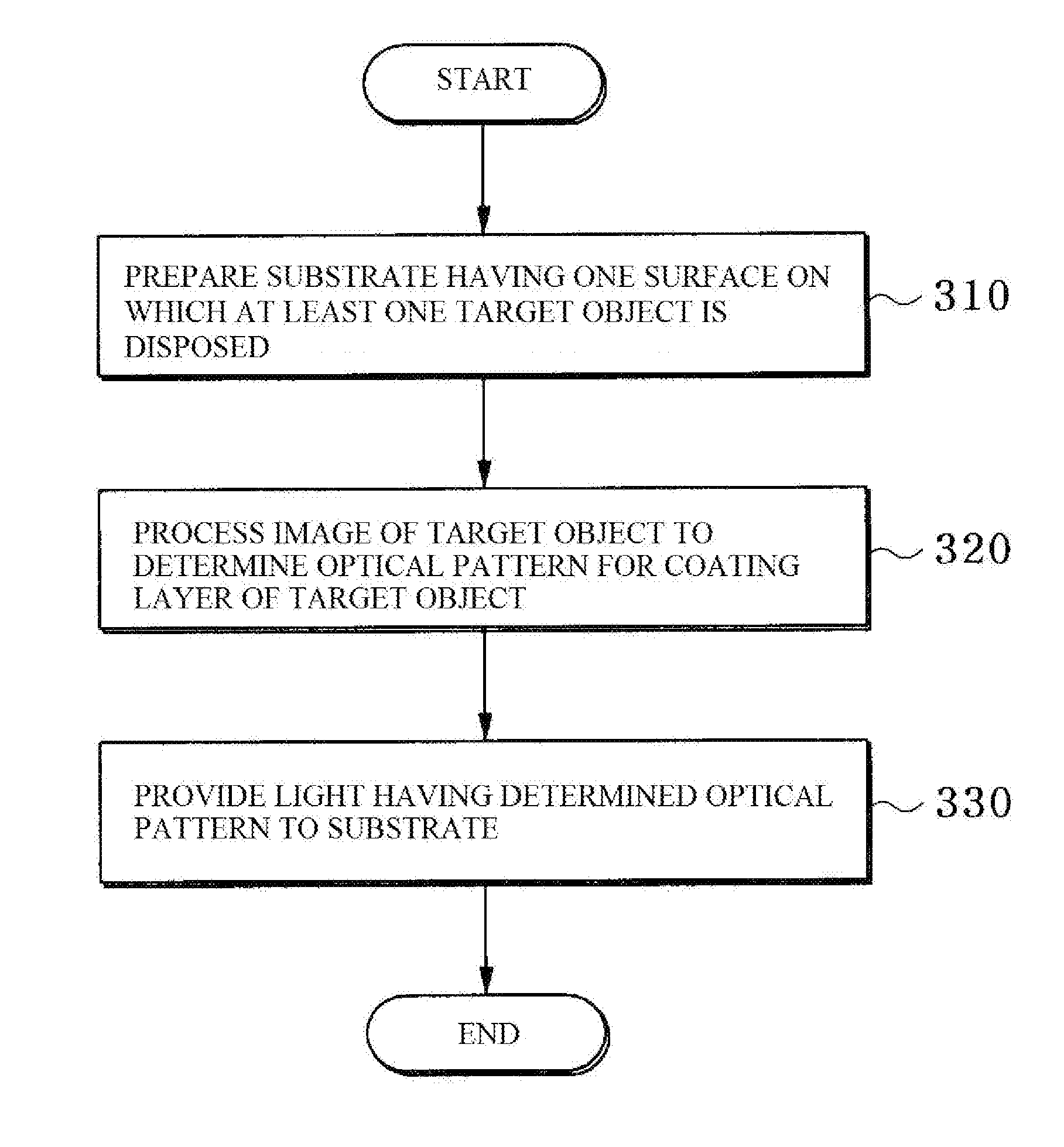
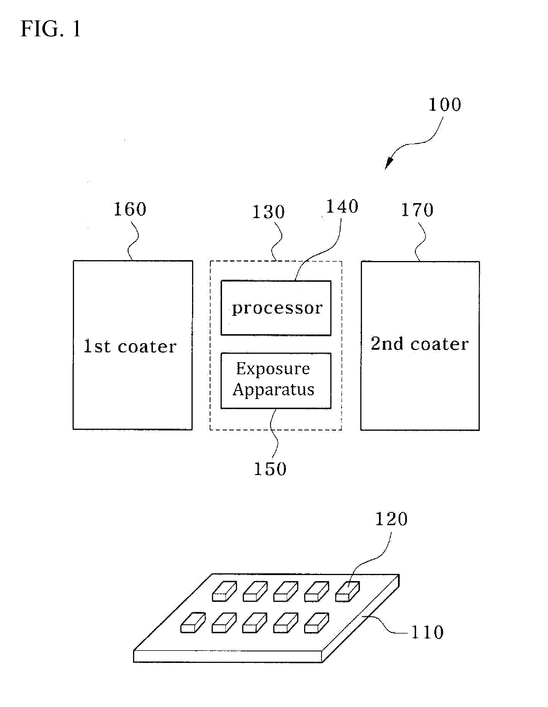
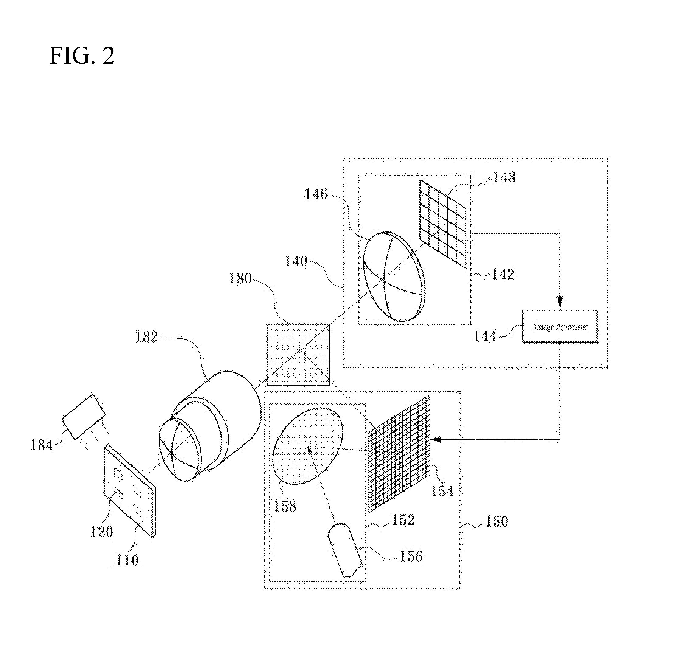
Image processing-based lithography system and method of coating target object
PatentActiveUS20160145744A1
Innovation
- A lithography system that includes a processor to process images of target objects and determine optical patterns for coating layers, allowing for the formation of patterns on substrates without photomasks, combined with a flexible substrate that can be deformed to change chip arrangements and a system for selectively exposing photoresist to light to form coating layers.
Method for coating chips
PatentActiveUS11955585B2
Innovation
- A method involving the formation of a photosensitive coating film using a photolithographic sequence with ultraviolet radiation to selectively remove the coating film, keeping it only at inter-chip spaces and avoiding mechanical abrasion, allowing for reduced thermal budgets and preserving chip integrity.
Material Science Advancements for Neural-Inspired Computing
Material science has undergone significant transformations in recent years, particularly in applications supporting neuromorphic computing. Advanced coating techniques have emerged as critical enablers for neural-inspired chip architectures, offering enhanced performance, reliability, and functionality. These developments represent a convergence of materials engineering, nanotechnology, and computational design principles.
The evolution of coating materials for neuromorphic applications has progressed from conventional silicon-based insulators to complex multi-functional layers incorporating novel nanomaterials. Carbon-based materials, including graphene and carbon nanotubes, have demonstrated exceptional electrical properties and thermal stability when applied as protective or conductive coatings on neuromorphic substrates.
Phase-change materials (PCMs) represent another breakthrough, enabling memristive behavior through reversible structural transitions between amorphous and crystalline states. These materials, typically chalcogenide-based compounds like Ge₂Sb₂Te₅, can be precisely deposited using advanced physical vapor deposition techniques to create non-volatile memory elements that mimic synaptic plasticity.
Metal-oxide thin films have gained prominence for their tunable resistive switching characteristics. Materials such as HfO₂, TiO₂, and Ta₂O₅ can be engineered at the nanoscale to exhibit controlled ionic migration, enabling analog resistance states that parallel biological synaptic weight changes. Recent advancements in atomic layer deposition have enabled precise control over film thickness and composition, critical for consistent device performance.
Biomimetic coating approaches represent the frontier of neuromorphic materials science. Researchers have developed organic-inorganic hybrid coatings that incorporate biological molecules or biomimetic polymers to create interfaces with enhanced biocompatibility and novel sensing capabilities. These materials bridge the gap between electronic systems and biological neural networks, potentially enabling direct neural interfaces.
Self-healing coating technologies have emerged as a solution to reliability challenges in neuromorphic systems. Drawing inspiration from biological systems, these materials incorporate microcapsules or vascular networks containing healing agents that can repair damage autonomously, extending device lifetime and maintaining performance integrity under operational stress.
The miniaturization trend in neuromorphic computing has driven innovations in ultra-thin coating technologies, with researchers achieving functional layers just a few atoms thick. These atomically precise coatings maintain electrical isolation while minimizing spatial requirements, enabling higher integration densities and more complex neural network implementations in hardware.
Environmental Impact of Coating Processes and Sustainability Measures
The coating processes employed in neuromorphic chip manufacturing present significant environmental challenges that warrant careful consideration. Traditional coating methods often involve the use of hazardous chemicals, including volatile organic compounds (VOCs), heavy metals, and various solvents that pose risks to both environmental and human health. Particularly concerning are physical vapor deposition (PVD) and chemical vapor deposition (CVD) techniques, which typically consume substantial energy and may release greenhouse gases such as perfluorocarbons and sulfur hexafluoride that have high global warming potential.
Water consumption represents another critical environmental concern, with wet coating processes requiring large volumes of ultra-pure water for cleaning and processing. This not only depletes water resources but also generates contaminated wastewater that requires specialized treatment before discharge. Additionally, the energy-intensive nature of many coating technologies, particularly those requiring high temperatures or vacuum conditions, contributes significantly to the carbon footprint of neuromorphic chip production.
In response to these challenges, the industry has begun implementing various sustainability measures. Material substitution has emerged as a promising approach, with manufacturers increasingly replacing toxic substances with environmentally benign alternatives. For instance, water-based solutions are gradually supplanting solvent-based coatings, while lead-free and cadmium-free materials are being adopted to reduce heavy metal contamination.
Process optimization represents another key sustainability strategy. Advanced equipment designs now incorporate closed-loop systems that recover and recycle solvents, significantly reducing waste generation. Similarly, precision application technologies minimize material usage while maintaining coating quality, thereby decreasing both resource consumption and waste production.
Energy efficiency improvements have also gained traction, with manufacturers implementing heat recovery systems and transitioning to renewable energy sources. Low-temperature coating processes are being developed to reduce energy requirements, while equipment modifications focus on minimizing idle time and optimizing power consumption during operation.
Regulatory frameworks increasingly influence coating practices, with legislation such as the Restriction of Hazardous Substances (RoHS) directive and Registration, Evaluation, Authorization and Restriction of Chemicals (REACH) regulations driving the adoption of greener technologies. Industry certifications like ISO 14001 further encourage manufacturers to implement environmental management systems that address the full lifecycle impact of their coating processes.
Looking forward, emerging technologies offer promising pathways to more sustainable coating practices. Atomic layer deposition (ALD) provides exceptional material efficiency through precise monolayer control, while biomimetic approaches inspired by natural processes may eventually enable ambient-temperature coating with minimal environmental impact. These innovations, coupled with ongoing industry commitment to sustainability, suggest a positive trajectory toward environmentally responsible neuromorphic chip production.
Unlock deeper insights with Patsnap Eureka Quick Research — get a full tech report to explore trends and direct your research. Try now!
Generate Your Research Report Instantly with AI Agent
Supercharge your innovation with Patsnap Eureka AI Agent Platform!