Why Neuromorphic Chips Are Essential for Next-Gen Communication
OCT 9, 20259 MIN READ
Generate Your Research Report Instantly with AI Agent
Patsnap Eureka helps you evaluate technical feasibility & market potential.
Neuromorphic Computing Evolution and Objectives
Neuromorphic computing represents a paradigm shift in computational architecture, drawing inspiration from the structure and function of the human brain. This approach emerged in the late 1980s when Carver Mead introduced the concept of using electronic analog circuits to mimic neuro-biological architectures. Since then, neuromorphic computing has evolved through several distinct phases, each marked by significant technological breakthroughs and expanding applications.
The initial phase focused primarily on theoretical foundations and basic circuit designs that could replicate neural behaviors. By the early 2000s, research institutions began developing more sophisticated neuromorphic systems, such as IBM's TrueNorth and the European Human Brain Project's SpiNNaker, which demonstrated the feasibility of large-scale neural network implementations in hardware.
Recent years have witnessed an acceleration in neuromorphic chip development, driven by the limitations of traditional von Neumann architectures in handling AI workloads efficiently. Companies like Intel (with its Loihi chip), BrainChip, and startups such as Rain Neuromorphics have made substantial advances in commercializing neuromorphic technology, moving beyond research prototypes to practical computing solutions.
The evolution trajectory points toward increasingly sophisticated systems that combine digital and analog processing elements, with greater density of artificial neurons and synapses, and enhanced capabilities for online learning and adaptation. This progression aligns with the growing need for edge computing solutions that can process sensory data with minimal power consumption.
The primary objectives of neuromorphic computing in the context of next-generation communication systems are multifaceted. First, these chips aim to dramatically reduce power consumption compared to traditional processors when handling neural network tasks, enabling AI capabilities in power-constrained environments like IoT devices and mobile networks.
Second, neuromorphic architectures seek to enable real-time processing of complex sensory data streams with minimal latency, a critical requirement for applications such as autonomous vehicles, smart infrastructure, and advanced telecommunications systems where milliseconds matter.
Third, these systems target inherent fault tolerance and adaptability, allowing communication networks to maintain functionality despite component failures or changing environmental conditions. This resilience is particularly valuable in mission-critical communication infrastructure.
Finally, neuromorphic computing aims to facilitate continuous learning capabilities directly in hardware, enabling communication systems to evolve and improve their performance over time without requiring constant retraining or updates from centralized servers, thus supporting truly intelligent edge computing.
Market Demand for Advanced Communication Systems
The global telecommunications market is experiencing unprecedented growth, driven by the exponential increase in data traffic, connected devices, and emerging applications requiring real-time processing capabilities. Current market research indicates that global data traffic is doubling approximately every 18-24 months, creating immense pressure on existing communication infrastructure. This surge in demand necessitates communication systems that can process massive amounts of data with minimal latency and energy consumption.
Traditional semiconductor technologies are approaching their physical limits in meeting these escalating requirements. Communication service providers report that power consumption in data centers has become a critical constraint, with cooling systems accounting for nearly 40% of total energy usage. This energy inefficiency represents both an economic and environmental challenge that must be addressed through innovative hardware solutions.
The emergence of 5G and future 6G networks is fundamentally transforming market expectations for communication systems. These next-generation networks demand ultra-reliable low-latency communication (URLLC) capabilities that current chip architectures struggle to deliver efficiently. Industry analysts project the global 5G infrastructure market to grow at a compound annual rate exceeding 30% through 2028, creating substantial opportunities for advanced chip technologies.
Edge computing represents another significant market driver for neuromorphic computing in communications. The trend toward processing data closer to its source rather than in centralized cloud facilities is gaining momentum across industries. Market forecasts suggest that by 2025, over 75% of enterprise-generated data will be processed at the edge, compared to just 10% today. This shift demands communication systems with unprecedented energy efficiency and real-time processing capabilities.
Artificial intelligence and machine learning applications in telecommunications are creating additional market pull for neuromorphic solutions. Network optimization, predictive maintenance, security threat detection, and autonomous network management all require sophisticated pattern recognition capabilities. The telecommunications AI market is expanding rapidly as operators seek to enhance service quality while reducing operational costs.
The Internet of Things (IoT) ecosystem presents perhaps the most compelling market case for neuromorphic chips in communications. With tens of billions of connected devices generating continuous data streams, conventional computing architectures cannot scale efficiently. The market demands communication systems that can intelligently filter, process, and transmit only relevant information, dramatically reducing bandwidth requirements and power consumption.
Regulatory pressures and sustainability initiatives are further accelerating market demand for energy-efficient communication technologies. Many countries have established carbon reduction targets that directly impact telecommunications operators, creating market incentives for adopting more efficient hardware solutions like neuromorphic chips.
Current Limitations in Communication Chip Technologies
Despite significant advancements in communication chip technologies, current solutions face substantial limitations that impede the development of next-generation communication systems. Traditional von Neumann architecture-based chips struggle with the exponentially increasing data volumes in modern networks, creating bottlenecks between processing and memory components. This "memory wall" results in significant latency issues and energy inefficiency, particularly problematic for real-time applications requiring instantaneous data processing.
Power consumption represents another critical limitation. Current communication chips consume excessive energy, making them unsuitable for edge devices with limited power resources. As networks expand to accommodate billions of IoT devices, this energy inefficiency becomes increasingly unsustainable, both economically and environmentally. The telecommunications industry already accounts for approximately 3-4% of global electricity consumption, a figure projected to rise dramatically without fundamental architectural changes.
Scalability challenges further constrain existing technologies. As communication networks grow in complexity and density, traditional chips struggle to maintain performance while managing increased computational demands. This limitation becomes particularly evident in scenarios requiring dynamic network reconfiguration or adaptive processing based on changing traffic patterns.
Current chips also demonstrate limited parallelism capabilities. While modern communication requires simultaneous processing of multiple data streams and protocols, conventional architectures process information sequentially, creating performance bottlenecks. This sequential processing model fails to efficiently handle the inherently parallel nature of communication network traffic.
Adaptability represents another significant shortcoming. Today's rigid chip designs lack the flexibility to efficiently adjust to varying workloads or evolving communication standards. This inflexibility necessitates frequent hardware replacements, increasing operational costs and environmental impact through electronic waste generation.
Signal processing limitations further constrain performance in complex electromagnetic environments. Current chips struggle with real-time interference mitigation, spectrum management, and adaptive modulation techniques essential for maximizing channel capacity in congested wireless environments.
Finally, artificial intelligence integration remains challenging with conventional architectures. As communication systems increasingly rely on AI for optimization, security, and autonomous operation, the fundamental mismatch between traditional computing architectures and neural processing creates significant inefficiencies in implementing these critical capabilities.
These limitations collectively highlight the urgent need for alternative computing paradigms like neuromorphic chips, which offer inherent advantages in parallelism, energy efficiency, and adaptability—qualities essential for meeting the demands of next-generation communication systems.
Current Neuromorphic Solutions for Communication Networks
01 Neuromorphic architecture design and implementation
Neuromorphic chips are designed to mimic the structure and functionality of the human brain, using specialized architectures that integrate processing and memory. These designs typically incorporate neural networks, synaptic connections, and spike-based processing to achieve brain-like computation. The architecture enables efficient parallel processing, low power consumption, and the ability to learn and adapt from input data, making them suitable for artificial intelligence applications.- Neuromorphic architecture design and implementation: Neuromorphic chips are designed to mimic the structure and function of the human brain, using specialized architectures that integrate processing and memory. These designs typically incorporate neural networks, synaptic connections, and spike-based processing to achieve brain-like computation. The architecture may include multiple layers of artificial neurons interconnected through programmable synapses, enabling efficient parallel processing and learning capabilities similar to biological neural systems.
- Memristor-based neuromorphic computing: Memristors are used in neuromorphic chips to simulate synaptic behavior, offering advantages in power efficiency and density. These devices can change their resistance based on the history of current flow, making them ideal for implementing synaptic weights in neural networks. Memristor-based neuromorphic systems can perform both computation and memory functions in the same physical location, reducing the energy consumption associated with data movement between separate processing and memory units.
- Spiking neural networks for neuromorphic computing: Spiking neural networks (SNNs) are a key component of neuromorphic chips, using discrete spikes for information processing similar to biological neurons. These networks operate on an event-driven basis, activating only when receiving sufficient input stimulation, which significantly reduces power consumption compared to traditional neural networks. SNNs enable efficient processing of temporal data and can be implemented using various hardware approaches to achieve brain-inspired computing with improved energy efficiency.
- Energy-efficient neuromorphic hardware: Energy efficiency is a primary focus in neuromorphic chip design, achieved through specialized circuits and processing techniques. These chips often operate at lower power by using event-driven computation, where processing occurs only when necessary rather than continuously. Various techniques such as analog computing, low-precision arithmetic, and specialized power management are employed to minimize energy consumption while maintaining computational capabilities, making neuromorphic systems suitable for edge computing and battery-powered applications.
- Applications and integration of neuromorphic systems: Neuromorphic chips are being integrated into various applications including computer vision, pattern recognition, autonomous systems, and sensory processing. These chips excel at tasks requiring real-time processing of sensory data, learning from experience, and adapting to new environments. The integration often involves specialized interfaces between conventional computing systems and neuromorphic hardware, allowing for hybrid computing approaches that leverage the strengths of both paradigms for complex cognitive tasks and artificial intelligence applications.
02 Materials and fabrication techniques for neuromorphic devices
Advanced materials and fabrication techniques are essential for creating efficient neuromorphic chips. These include the use of memristive materials, phase-change materials, and other novel semiconductors that can mimic synaptic behavior. Specialized manufacturing processes enable the integration of these materials into functional neuromorphic systems, allowing for the creation of dense neural networks with low power requirements and high computational efficiency.Expand Specific Solutions03 Learning algorithms and training methods for neuromorphic systems
Neuromorphic chips require specialized learning algorithms and training methods that differ from traditional computing approaches. These include spike-timing-dependent plasticity (STDP), reinforcement learning, and other bio-inspired learning mechanisms. The algorithms enable neuromorphic systems to adapt to new data, recognize patterns, and make decisions based on experience, similar to biological neural networks. These methods are designed to work efficiently with the unique architecture of neuromorphic hardware.Expand Specific Solutions04 Power efficiency and optimization techniques
A key advantage of neuromorphic chips is their potential for extremely low power consumption compared to traditional computing architectures. Various techniques are employed to optimize power efficiency, including event-driven processing, sparse coding, and specialized circuit designs that minimize energy use during computation. These approaches enable neuromorphic systems to perform complex AI tasks with significantly reduced energy requirements, making them suitable for edge computing and battery-powered devices.Expand Specific Solutions05 Applications and integration of neuromorphic computing
Neuromorphic chips are being applied across various domains including computer vision, natural language processing, autonomous systems, and sensor networks. These applications leverage the unique capabilities of neuromorphic computing such as real-time processing, pattern recognition, and adaptive learning. Integration techniques allow neuromorphic systems to work alongside traditional computing architectures or as standalone solutions for specific AI tasks, enabling more efficient and capable intelligent systems.Expand Specific Solutions
Leading Companies in Neuromorphic Chip Industry
Neuromorphic chips are emerging as critical components for next-generation communication systems, positioned at the intersection of early commercial deployment and rapid innovation. The market is experiencing significant growth, projected to reach substantial scale as these brain-inspired processors address power and latency challenges in edge computing. Companies like Syntiant, IBM, and Samsung are leading commercial deployment with ultra-low-power solutions, while research institutions including Tsinghua University and KAIST are advancing fundamental architectures. Intel, Western Digital, and Polyn Technology are developing specialized applications for data centers and IoT devices. The competitive landscape features both established semiconductor giants and agile startups, with partnerships between industry and academia accelerating development of neuromorphic solutions that promise to revolutionize AI processing in communication networks.
International Business Machines Corp.
Technical Solution: IBM's neuromorphic chip technology, particularly its TrueNorth architecture, represents a significant advancement for next-generation communication systems. TrueNorth employs a non-von Neumann architecture that mimics the brain's neural structure with 1 million programmable neurons and 256 million synapses. This design enables parallel processing of massive data streams with remarkable energy efficiency - consuming only 70mW during operation, which is orders of magnitude more efficient than conventional processors. For communication applications, IBM has developed specialized neuromorphic solutions that can process natural language, speech recognition, and complex signal processing tasks in real-time while maintaining minimal latency. Their neuromorphic systems incorporate spike-based computing principles that allow for asynchronous event-driven processing, which is particularly valuable for handling the bursty nature of modern communication traffic. IBM has also demonstrated neuromorphic implementations for 5G and beyond, where these chips can adaptively manage spectrum allocation, perform intelligent beamforming, and optimize network resources dynamically based on usage patterns and environmental conditions.
Strengths: Exceptional energy efficiency (70mW operation) makes IBM's neuromorphic chips ideal for deployment in distributed communication infrastructure. The event-driven architecture significantly reduces power consumption during idle periods while maintaining rapid response capabilities. Weaknesses: Programming complexity remains a challenge as developers must adapt to non-traditional computing paradigms. Integration with existing communication infrastructure requires significant adaptation of protocols and interfaces.
Samsung Electronics Co., Ltd.
Technical Solution: Samsung has developed advanced neuromorphic chip solutions specifically targeting next-generation communication systems. Their approach integrates memory and processing in a single architecture, significantly reducing the energy consumption and latency issues that plague conventional von Neumann architectures. Samsung's neuromorphic chips utilize resistive RAM (RRAM) technology to implement artificial synapses, achieving analog-like computation with digital precision. This enables efficient processing of the complex, time-varying signals characteristic of modern communication systems. The company has demonstrated neuromorphic implementations that can process multiple communication protocols simultaneously while dynamically adapting to changing network conditions. Samsung's neuromorphic solutions incorporate on-chip learning capabilities that allow communication systems to continuously optimize performance based on real-world usage patterns and interference. For 5G and beyond applications, Samsung has shown their neuromorphic technology can perform complex signal processing tasks such as channel estimation, precoding, and interference cancellation with significantly reduced power consumption compared to traditional DSP approaches. Their chips achieve this while maintaining the ultra-low latency requirements (sub-millisecond) essential for next-generation communication applications like autonomous vehicle communications, industrial IoT, and augmented reality.
Strengths: Samsung's vertical integration of memory and processing technologies gives them unique advantages in neuromorphic design. Their established position in the mobile and network equipment markets provides clear pathways to commercial deployment. Weaknesses: Current implementations still face challenges with standardization and interoperability with existing communication infrastructure. The technology requires specialized programming approaches that may limit initial adoption.
Key Patents and Research in Neuromorphic Signal Processing
Producing spike-timing dependent plasticity in a neuromorphic network utilizing phase change synaptic devices
PatentActiveUS20180197074A1
Innovation
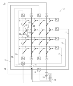
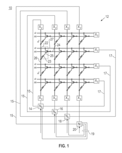
- A neuromorphic network utilizing Phase Change Memory (PCM) synaptic devices with variable state resistors and transistor devices, coupled with a timing controller to generate phased operations, enabling spike-timing dependent plasticity by changing synaptic conductance based on the relative spike times of pre-synaptic and post-synaptic neurons.
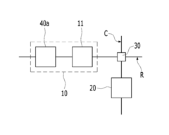
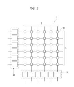
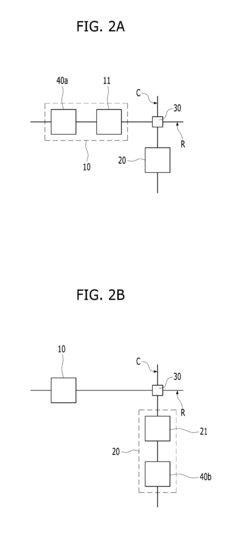
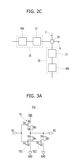
Neuromorphic device having inverting circuits
PatentActiveUS20180314929A1
Innovation
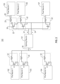
- The neuromorphic device incorporates a post-synaptic neuron with a transfer function circuit that includes a series connection of inverting circuits with varying numbers and types of pull-up and pull-down transistors, allowing for smooth output signal changes, such as sigmoid curves, by electrically connecting drain electrodes and bodies of transistors, thereby enhancing the interpretation of multiple levels in synapse weights and input data patterns.
Energy Efficiency Implications of Neuromorphic Computing
Neuromorphic computing represents a paradigm shift in energy consumption patterns for computational systems. Traditional von Neumann architectures require significant power for data movement between memory and processing units, creating a bottleneck that becomes increasingly problematic as communication networks expand. Neuromorphic chips, by contrast, mimic the brain's architecture where memory and processing are co-located, dramatically reducing energy requirements for data transfer operations.
The energy efficiency advantages of neuromorphic computing are particularly compelling when examining next-generation communication requirements. Current 5G networks already consume approximately 3-4 times more energy than their 4G predecessors, and projections for 6G suggest exponential increases in energy demand. Neuromorphic solutions offer potential energy savings of 100-1000x compared to conventional computing approaches for similar communication processing tasks.
This efficiency stems from several architectural innovations. Spike-based processing allows neuromorphic systems to operate with extremely low power consumption during periods of inactivity, activating circuits only when information needs processing. Additionally, the massively parallel architecture distributes computational load across numerous simple processing elements rather than relying on a few power-hungry central processors.
Real-world implementations have demonstrated these efficiency gains. IBM's TrueNorth neuromorphic chip processes sensory data at less than 100mW, while Intel's Loihi chip demonstrates 1000x better energy efficiency than conventional GPUs for certain communication-relevant tasks like sparse coding and pattern recognition. These improvements become particularly significant when considering edge computing applications in communication networks, where power constraints often limit deployment options.
Beyond raw power consumption metrics, neuromorphic computing also addresses thermal management challenges that plague conventional high-performance computing systems. Lower heat generation reduces cooling requirements, further decreasing the total energy footprint of communication infrastructure. This characteristic becomes increasingly valuable as communication networks expand into remote or resource-constrained environments.
The transition to neuromorphic computing also aligns with broader sustainability goals in the telecommunications industry. As data traffic continues its exponential growth trajectory, the energy efficiency of neuromorphic systems offers a path to more sustainable network expansion. Industry analysts project that implementing neuromorphic processing elements at key network nodes could reduce overall network energy consumption by 30-40% while maintaining or improving performance for critical communication functions.
Integration Challenges with Existing Network Infrastructure
The integration of neuromorphic chips into existing network infrastructure presents significant challenges that must be addressed before widespread adoption can occur. Current network architectures are optimized for traditional computing paradigms, creating fundamental compatibility issues with the event-driven, spike-based processing nature of neuromorphic systems. These architectural differences necessitate substantial modifications to interface protocols, data formatting, and communication methodologies.
Power management represents another critical integration hurdle. While neuromorphic chips offer superior energy efficiency for specific computational tasks, their integration into existing networks requires sophisticated power delivery systems and thermal management solutions. Network infrastructure designed for consistent power consumption patterns must adapt to the variable power profiles characteristic of neuromorphic processing.
Data conversion between conventional binary formats and the temporal, spike-based encoding used by neuromorphic systems creates substantial overhead. This conversion process introduces latency and computational costs that can potentially offset the performance advantages of neuromorphic computing, particularly in real-time communication applications where millisecond delays impact service quality.
Legacy software ecosystems present equally formidable barriers. The vast majority of network management tools, monitoring systems, and security protocols are designed for traditional computing architectures. Developing neuromorphic-compatible versions of these essential software components requires significant investment and expertise in both neuromorphic principles and network engineering.
Standardization remains notably absent in the neuromorphic computing landscape. Without established industry standards for neuromorphic chip integration, network equipment manufacturers face uncertainty when implementing support for these novel processors. This standardization gap slows adoption and creates market fragmentation that impedes economies of scale.
Testing and validation methodologies for neuromorphic systems within communication networks are still in their infancy. Traditional network performance metrics and testing procedures do not adequately capture the unique operational characteristics of neuromorphic processing, creating challenges for quality assurance and performance optimization in hybrid systems.
Transitional strategies represent perhaps the most practical near-term approach, with hybrid architectures that incorporate neuromorphic accelerators alongside conventional processors. These hybrid systems allow organizations to gradually integrate neuromorphic capabilities while maintaining compatibility with existing network infrastructure, providing a bridge to more comprehensive neuromorphic integration in future network generations.
Unlock deeper insights with Patsnap Eureka Quick Research — get a full tech report to explore trends and direct your research. Try now!
Generate Your Research Report Instantly with AI Agent
Supercharge your innovation with Patsnap Eureka AI Agent Platform!
