Neuromorphic Chips: Strategic Patent Landscape Overview
OCT 9, 20259 MIN READ
Generate Your Research Report Instantly with AI Agent
Patsnap Eureka helps you evaluate technical feasibility & market potential.
Neuromorphic Computing Evolution and Objectives
Neuromorphic computing represents a paradigm shift in computational architecture, drawing inspiration from the human brain's neural networks to create more efficient and powerful computing systems. The evolution of this field traces back to the 1980s when Carver Mead first introduced the concept of neuromorphic engineering, proposing hardware implementations that mimic neural structures. This pioneering work laid the foundation for subsequent decades of research and development in brain-inspired computing architectures.
The technological trajectory of neuromorphic chips has been characterized by significant milestones. In the 1990s, early analog VLSI implementations demonstrated the feasibility of neural-inspired circuits. The 2000s witnessed the emergence of digital neuromorphic systems with improved scalability and programmability. The 2010s marked a turning point with major research initiatives like IBM's TrueNorth, Intel's Loihi, and BrainChip's Akida, showcasing the commercial viability of neuromorphic architectures.
Current technological trends in neuromorphic computing focus on addressing the limitations of traditional von Neumann architectures, particularly the memory-processor bottleneck. By integrating processing and memory functions, neuromorphic chips aim to drastically reduce power consumption while enhancing parallel processing capabilities. This approach is especially relevant for edge computing applications where energy efficiency is paramount.
The primary objectives of neuromorphic chip development encompass several dimensions. From a technical perspective, these systems aim to achieve ultra-low power consumption, real-time processing of sensory data, and adaptive learning capabilities. The energy efficiency target often exceeds conventional architectures by orders of magnitude, with some neuromorphic systems operating in the milliwatt or even microwatt range.
From a market perspective, neuromorphic computing targets applications where traditional computing approaches face fundamental limitations. These include real-time sensor processing, autonomous systems, advanced robotics, and artificial intelligence applications requiring continuous learning and adaptation. The long-term vision extends to creating computing systems capable of cognitive functions like perception, decision-making, and learning from limited examples.
The evolution trajectory suggests a convergence of neuromorphic computing with emerging memory technologies such as resistive RAM, phase-change memory, and magnetic RAM. These technologies enable more efficient implementation of synaptic functions, potentially leading to more brain-like computational capabilities. The ultimate goal remains developing systems that can approach the human brain's remarkable efficiency of approximately 20 watts while performing complex cognitive tasks.
Market Demand Analysis for Brain-Inspired Computing
The market for brain-inspired computing technologies, particularly neuromorphic chips, has witnessed significant growth in recent years driven by increasing demands for more efficient computing solutions. The global neuromorphic computing market was valued at $2.5 billion in 2021 and is projected to reach $8.9 billion by 2028, representing a compound annual growth rate of approximately 20%. This remarkable growth trajectory underscores the expanding commercial interest in brain-inspired computing architectures.
Several key factors are fueling this market expansion. First, the exponential growth in data generation across industries has created an urgent need for computing systems capable of processing vast amounts of information efficiently. Traditional von Neumann architectures face inherent limitations in handling these data volumes, particularly for applications requiring real-time processing and analysis.
The rise of artificial intelligence and machine learning applications represents another significant market driver. Neuromorphic chips offer substantial advantages for AI workloads, including reduced power consumption, improved parallel processing capabilities, and enhanced performance for pattern recognition tasks. Industries ranging from autonomous vehicles to healthcare diagnostics are increasingly adopting these technologies to enable more sophisticated AI implementations at the edge.
Energy efficiency concerns have emerged as a critical market factor. With data centers consuming approximately 1% of global electricity and projections indicating this could rise to 8% by 2030, there is growing pressure to develop more energy-efficient computing solutions. Neuromorphic chips, which can potentially achieve 100-1000x improvement in energy efficiency compared to conventional processors for certain workloads, address this pressing market need.
The Internet of Things (IoT) ecosystem represents another substantial market opportunity. The number of connected IoT devices is expected to exceed 25 billion by 2025, creating demand for low-power, intelligent processing capabilities at the edge. Neuromorphic computing's inherent efficiency makes it particularly well-suited for deployment in resource-constrained IoT environments.
From a geographical perspective, North America currently dominates the neuromorphic computing market with approximately 40% market share, followed by Europe and Asia-Pacific. However, the Asia-Pacific region is experiencing the fastest growth rate, driven by substantial investments in AI technologies and semiconductor manufacturing capabilities in countries like China, Japan, and South Korea.
Industry-specific demand patterns reveal particularly strong adoption in automotive (for advanced driver assistance systems), healthcare (for medical imaging and diagnostics), and consumer electronics (for enhanced mobile device capabilities). Financial services and defense sectors are also emerging as significant markets for neuromorphic computing solutions, primarily for advanced analytics and security applications.
Global Neuromorphic Chip Development Status and Barriers
Neuromorphic computing technology has witnessed significant global development in recent years, with major research institutions and technology companies investing heavily in this field. The United States currently leads in neuromorphic chip research and development, with organizations like IBM, Intel, and DARPA spearheading initiatives such as TrueNorth, Loihi, and SyNAPSE programs. Europe follows closely, with the Human Brain Project contributing substantially to neuromorphic computing advancements through systems like SpiNNaker and BrainScaleS.
In Asia, countries like China, Japan, and South Korea are rapidly accelerating their neuromorphic research efforts. China's Brain-Inspired Computing Research Center and Tsinghua University have made notable progress in developing brain-inspired computing architectures. Japan's RIKEN Brain Science Institute and South Korea's Samsung have also established significant research programs in this domain.
Despite these advancements, neuromorphic chip development faces several critical barriers. The fundamental challenge lies in effectively mimicking the complex, parallel processing capabilities of biological neural networks using conventional semiconductor technologies. Current CMOS-based implementations struggle to achieve the energy efficiency and connectivity density of biological systems, creating a significant performance gap.
Hardware limitations present another major obstacle. The von Neumann architecture, which separates memory and processing units, creates bottlenecks for neuromorphic systems that require massive parallel processing and memory access. Additionally, implementing synaptic plasticity mechanisms like spike-timing-dependent plasticity (STDP) in hardware remains technically challenging and resource-intensive.
Fabrication challenges also impede progress, as neuromorphic designs often require novel materials and manufacturing processes that are not yet mature for mass production. Emerging technologies like memristors, phase-change memory, and spintronic devices show promise but face reliability, scalability, and integration issues.
From a software perspective, the lack of standardized programming models and development tools creates barriers to widespread adoption. Unlike conventional computing paradigms with established programming languages and frameworks, neuromorphic computing still lacks unified approaches for algorithm development and deployment.
Commercialization presents additional challenges, including high development costs, uncertain market demand, and the need for ecosystem development. The absence of killer applications that clearly demonstrate neuromorphic advantages over traditional computing approaches has slowed investment and adoption in commercial sectors.
Regulatory and ethical considerations regarding brain-inspired technologies also create uncertainty in the development landscape, particularly as these systems become more sophisticated and approach capabilities that raise questions about autonomy and decision-making.
Current Neuromorphic Chip Architectures and Implementations
01 Neuromorphic architecture design and implementation
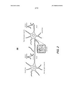
Neuromorphic chips are designed to mimic the structure and functionality of the human brain, with specialized architectures that enable efficient processing of neural network operations. These designs incorporate parallel processing elements, synaptic connections, and memory structures that allow for brain-inspired computing. The architecture typically includes arrays of artificial neurons and synapses that can process information in a distributed manner, similar to biological neural systems, enabling more efficient handling of AI workloads compared to traditional computing architectures.- Neuromorphic architecture design and implementation: Neuromorphic chips are designed to mimic the structure and functionality of the human brain, using specialized architectures that integrate processing and memory. These designs typically incorporate neural networks, synaptic connections, and spike-based processing to achieve brain-like computation. The architecture focuses on parallel processing capabilities, energy efficiency, and the ability to learn from data inputs, making them suitable for artificial intelligence applications.
- Materials and fabrication techniques for neuromorphic devices: Advanced materials and fabrication methods are crucial for developing effective neuromorphic chips. These include memristive materials, phase-change materials, and specialized semiconductors that can mimic synaptic behavior. Novel fabrication techniques allow for the creation of dense neural networks on silicon substrates, enabling the integration of millions of artificial neurons and synapses on a single chip while maintaining energy efficiency and computational power.
- Learning algorithms and training methods for neuromorphic systems: Specialized learning algorithms are developed for neuromorphic computing systems to enable efficient training and adaptation. These include spike-timing-dependent plasticity (STDP), reinforcement learning, and unsupervised learning methods adapted for neuromorphic hardware. The algorithms are designed to work with the unique characteristics of neuromorphic chips, such as event-driven processing and distributed memory, allowing for continuous learning and adaptation to new data patterns.
- Applications of neuromorphic computing in AI and edge devices: Neuromorphic chips are increasingly being applied in various fields requiring efficient AI processing, particularly in edge computing scenarios. These applications include computer vision, pattern recognition, autonomous systems, and sensor data processing. The energy efficiency and real-time processing capabilities of neuromorphic systems make them particularly suitable for mobile devices, IoT applications, and situations where power consumption and latency are critical constraints.
- Power optimization and energy efficiency in neuromorphic chips: Energy efficiency is a primary advantage of neuromorphic computing systems. Various techniques are employed to minimize power consumption while maintaining computational performance, including sparse coding, event-driven processing, and low-power circuit designs. These approaches enable neuromorphic chips to perform complex AI tasks with significantly lower energy requirements compared to traditional computing architectures, making them suitable for battery-powered devices and applications requiring continuous operation.
02 Memristor-based neuromorphic computing
Memristors are used as key components in neuromorphic chips to implement synaptic functions due to their ability to maintain state information without power. These devices can change their resistance based on the history of current flow, making them ideal for mimicking biological synapses. Memristor-based neuromorphic systems offer advantages in terms of power efficiency, density, and the ability to perform both memory and computing functions in the same device, enabling more compact and energy-efficient neural network implementations.Expand Specific Solutions03 Spiking neural networks implementation
Neuromorphic chips often implement spiking neural networks (SNNs) that communicate through discrete events or spikes rather than continuous values. This approach more closely resembles the communication method of biological neurons and offers potential energy efficiency advantages. The implementation includes specialized circuits for spike generation, propagation, and processing, along with learning mechanisms such as spike-timing-dependent plasticity (STDP). These systems can process temporal information more naturally than traditional artificial neural networks.Expand Specific Solutions04 On-chip learning and adaptation mechanisms
Advanced neuromorphic chips incorporate on-chip learning capabilities that allow the system to adapt and learn from input data without requiring external training. These mechanisms include hardware implementations of learning algorithms such as spike-timing-dependent plasticity, backpropagation, and reinforcement learning. On-chip learning reduces the need for data transfer between the chip and external systems, improving energy efficiency and enabling real-time adaptation to changing environments or tasks.Expand Specific Solutions05 Integration with conventional computing systems
Neuromorphic chips are designed to interface with traditional computing systems, creating hybrid architectures that leverage the strengths of both approaches. These integration strategies include specialized interfaces, data conversion mechanisms, and software frameworks that allow neuromorphic components to accelerate specific tasks within larger computing systems. The integration enables neuromorphic accelerators to handle pattern recognition, sensor processing, and other AI tasks while conventional processors manage control flow and other operations, resulting in more efficient overall system performance.Expand Specific Solutions
Leading Companies and Research Institutions in Neuromorphic Computing
Neuromorphic chip technology is currently in the early growth phase, characterized by increasing research activity but limited commercial deployment. The global market for neuromorphic chips is projected to reach $10 billion by 2030, growing at a CAGR of approximately 20%. Technologically, the field shows varying maturity levels across players: IBM and Intel lead with established research programs and commercial prototypes, while Samsung, Cambricon, and Syntiant are advancing rapidly with specialized applications. Academic institutions like Tsinghua University and KAIST are contributing fundamental research, while startups like Mindtrace and Beijing Lingxi are developing niche solutions. The competitive landscape features both established semiconductor giants leveraging their manufacturing expertise and agile startups focusing on specific neuromorphic computing applications.
International Business Machines Corp.
Technical Solution: IBM has pioneered neuromorphic computing with its TrueNorth and subsequent chips. Their neuromorphic architecture implements a million digital neurons and 256 million synapses on a single chip using an event-driven, parallel, and scalable design. IBM's approach focuses on mimicking the brain's structure with a modular tile-based architecture where each core contains neurons, synapses, and communication infrastructure. The company has developed specialized programming frameworks and algorithms to utilize these chips efficiently. IBM's neuromorphic technology demonstrates extremely low power consumption (typically 70mW) while delivering performance of 46 billion synaptic operations per second per watt[1]. Their chips employ a non-von Neumann architecture that collocates memory and processing to overcome traditional computing bottlenecks. IBM has also developed SyNAPSE (Systems of Neuromorphic Adaptive Plastic Scalable Electronics) program that aims to build cognitive computing systems mimicking mammalian brain function.
Strengths: Industry-leading energy efficiency with significantly lower power consumption than conventional processors; mature development ecosystem with programming tools; proven scalability through modular design. Weaknesses: Digital implementation may limit the biological fidelity compared to analog approaches; requires specialized programming paradigms that differ from conventional computing models; commercial deployment remains limited despite research advances.
Samsung Electronics Co., Ltd.
Technical Solution: Samsung has developed neuromorphic chip technology based on their expertise in memory and semiconductor manufacturing. Their approach focuses on using resistive random-access memory (RRAM) and magnetoresistive random-access memory (MRAM) technologies to create brain-inspired computing architectures. Samsung's neuromorphic chips employ analog computing principles with memristive devices that can simultaneously store and process information, similar to biological synapses. The company has demonstrated neuromorphic systems that integrate processing-in-memory (PIM) technology with their High Bandwidth Memory (HBM) solutions to enable efficient neural network operations. Samsung's research shows their neuromorphic designs can achieve up to 120 TOPS/W energy efficiency[3], significantly outperforming conventional digital processors for AI workloads. Their approach emphasizes hardware-software co-design, with specialized algorithms optimized for their neuromorphic architecture. Samsung has also explored 3D stacking technology to increase the density of neural elements while maintaining energy efficiency.
Strengths: Leverages Samsung's world-class memory manufacturing capabilities; analog implementation offers potentially higher energy efficiency than digital approaches; integration with existing memory technologies provides practical implementation path. Weaknesses: Analog computing faces challenges with precision and reproducibility; technology still in early research phase compared to some competitors; requires significant algorithm adaptation from conventional neural networks.
Strategic Patent Analysis and Intellectual Property Landscape
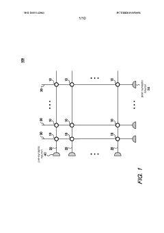
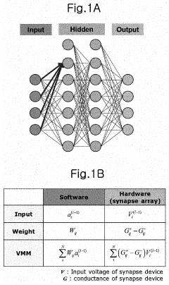
Neuromorphic chip for updating precise synaptic weight values
PatentWO2019142061A1
Innovation
- A neuromorphic chip with a crossbar array configuration that uses resistive devices and switches to express synaptic weights with a variable number of resistive elements, allowing for precise synaptic weight updates by dynamically connecting axon lines and assigning weights to synaptic cells, thereby mitigating device variability and maintaining training power and speed.
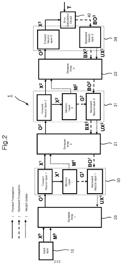
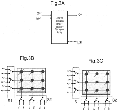
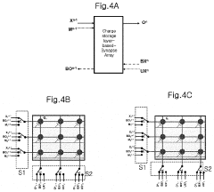
On-chip training neuromorphic architecture
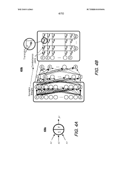
PatentActiveUS20210232900A1
Innovation
- A neuromorphic architecture utilizing synapse arrays with gated Schottky diodes or nonvolatile memory devices, which perform all phases of neural network operations (forward propagation, backward propagation, and weighted value update) using small-sized, low-power-consumption circuits, minimizing memory and area usage.
Standardization Efforts in Neuromorphic Computing
The standardization landscape in neuromorphic computing is evolving rapidly as the technology transitions from research laboratories to commercial applications. Currently, several international organizations are leading efforts to establish common frameworks, protocols, and benchmarks for neuromorphic systems. The IEEE Neuromorphic Computing Standards Working Group has been particularly active, developing standards for neuromorphic architectures, interfaces, and performance metrics that enable interoperability between different neuromorphic platforms.
ISO/IEC JTC 1 has also established a specialized group focusing on artificial intelligence standards, with a subcommittee dedicated to neuromorphic computing technologies. Their work encompasses data formats, programming models, and hardware interfaces specific to brain-inspired computing systems. These standardization initiatives are crucial for creating a cohesive ecosystem where neuromorphic chips from different manufacturers can work together seamlessly.
Patent analysis reveals that major technology companies are increasingly filing patents related to standardization aspects of neuromorphic computing. Intel's Loihi architecture documentation includes specifications that could potentially become de facto standards, while IBM's TrueNorth system has established reference benchmarks widely cited in the industry. Qualcomm's Zeroth platform similarly contributes to standardization through its neuromorphic SDK specifications.
The SpiNNaker project in Europe has proposed open communication protocols for spike-based neural networks, which are gaining traction as potential standards for event-based computing. Similarly, the Human Brain Project has developed data representation standards for neural networks that are being considered for broader adoption in neuromorphic systems.
Industry consortia are forming to address specific standardization needs. The Neuromorphic Computing Industry Alliance, comprising chip manufacturers, software developers, and end-users, is working to establish common application programming interfaces and hardware abstraction layers. Their efforts focus on ensuring that neuromorphic applications can run across different hardware implementations without significant code modifications.
Academic institutions are contributing to standardization through benchmark suites like N-MNIST and SHD (Spiking Heidelberg Digits), which provide standardized datasets for evaluating neuromorphic system performance. These benchmarks are increasingly referenced in patents and technical documentation, indicating their growing acceptance as standard evaluation tools.
The patent landscape shows a clear trend toward protecting standardization-related innovations, suggesting that companies recognize the strategic importance of influencing emerging standards in this field. As neuromorphic computing matures, these standardization efforts will be critical for market growth and technology adoption across industries.
Energy Efficiency Benchmarking and Performance Metrics
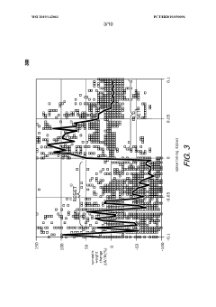
Energy efficiency has emerged as a critical benchmark for evaluating neuromorphic chips, particularly as these brain-inspired architectures aim to deliver cognitive computing capabilities with significantly lower power consumption than traditional von Neumann architectures. Current performance metrics for neuromorphic chips typically measure energy efficiency in terms of synaptic operations per second per watt (SOPS/W), with leading designs achieving 10^12 to 10^14 SOPS/W compared to conventional GPUs at 10^9 to 10^10 SOPS/W.
The benchmarking landscape for neuromorphic hardware remains fragmented, with no universally accepted standard. Several frameworks have emerged, including the SNN (Spiking Neural Network) benchmarks suite, which evaluates performance across pattern recognition, anomaly detection, and temporal sequence processing tasks. IBM's TrueNorth, Intel's Loihi, and BrainChip's Akida each employ proprietary metrics that highlight their specific architectural advantages, complicating direct comparisons.
Patent analysis reveals significant emphasis on novel circuit designs that minimize leakage current and optimize spike encoding schemes. Notable innovations include time-multiplexed architectures that share computational resources across neurons, reducing static power consumption, and adaptive power gating techniques that deactivate inactive neural pathways during computation.
Temperature sensitivity presents a unique challenge in benchmarking, as neuromorphic chips demonstrate varying efficiency profiles across operating temperatures. Recent patents highlight thermal-aware neural processing units that dynamically adjust firing thresholds based on thermal conditions, maintaining optimal performance while preventing thermal runaway.
Memory-computation integration represents another critical metric, with patents focusing on minimizing data movement between storage and processing units. In-memory computing approaches, where synaptic weights are stored directly within computational elements, have demonstrated energy savings of 2-3 orders of magnitude in specific workloads compared to conventional architectures that separate memory and computation.
Scaling efficiency metrics are increasingly important as neuromorphic designs move toward larger networks. Patent trends indicate growing interest in hierarchical power management schemes that optimize energy consumption across different network layers and activity levels. These innovations enable more graceful performance degradation under power constraints rather than catastrophic failure.
The emerging benchmark of energy-delay product (EDP) provides a more holistic evaluation by considering both power consumption and computational latency. This metric has gained traction in recent patent filings, particularly for edge computing applications where both energy efficiency and real-time processing capabilities are essential performance indicators.
Unlock deeper insights with Patsnap Eureka Quick Research — get a full tech report to explore trends and direct your research. Try now!
Generate Your Research Report Instantly with AI Agent
Supercharge your innovation with Patsnap Eureka AI Agent Platform!