

Research on Smart Neuromorphic Chips with Improved Efficiency
OCT 9, 20259 MIN READ
Generate Your Research Report Instantly with AI Agent
PatSnap Eureka helps you evaluate technical feasibility & market potential.
Neuromorphic Computing Background and Objectives
Neuromorphic computing represents a paradigm shift in computational architecture, drawing inspiration from the structure and function of the human brain. This field emerged in the late 1980s when Carver Mead introduced the concept of using electronic analog circuits to mimic neuro-biological architectures. Over the past three decades, neuromorphic computing has evolved from theoretical concepts to practical implementations, with significant advancements in materials science, circuit design, and computational algorithms contributing to its development.
The evolution of neuromorphic computing has been driven by the limitations of traditional von Neumann architecture, particularly in terms of energy efficiency and processing capabilities for complex cognitive tasks. Traditional computing systems face the "von Neumann bottleneck," where the separation between processing and memory units creates performance constraints. Neuromorphic systems address this by integrating memory and processing, similar to biological neural networks, enabling parallel processing and potentially dramatic improvements in energy efficiency.
Current technological trends in neuromorphic computing include the development of specialized hardware accelerators, integration of novel materials such as phase-change memory and memristors, and the implementation of spiking neural networks (SNNs) that more accurately replicate biological neural behavior. These advancements are converging toward creating computing systems that can perform complex cognitive tasks with significantly lower power consumption than conventional systems.
The primary objective of research on smart neuromorphic chips with improved efficiency is to develop computing systems that can process complex, unstructured data with energy efficiency approaching that of the human brain. The human brain operates on approximately 20 watts of power while performing sophisticated cognitive functions—a level of efficiency that remains unmatched by current artificial systems. Achieving comparable efficiency in neuromorphic chips would revolutionize applications in edge computing, autonomous systems, and real-time data processing.
Additional objectives include enhancing the scalability of neuromorphic architectures to support larger neural networks, improving the integration of these systems with conventional computing infrastructure, and developing programming paradigms that can effectively utilize the unique capabilities of neuromorphic hardware. These goals are driven by the potential applications in artificial intelligence, robotics, Internet of Things (IoT), and biomedical devices, where energy constraints and real-time processing requirements are critical factors.
The long-term vision for neuromorphic computing extends beyond mere efficiency improvements to creating systems capable of adaptive learning, self-organization, and fault tolerance—characteristics inherent to biological neural systems. This represents not just an incremental improvement in computing technology but potentially a fundamental shift in how computational problems are approached and solved.
Market Analysis for Energy-Efficient AI Hardware
The global market for energy-efficient AI hardware is experiencing unprecedented growth, driven by the increasing deployment of AI applications across various sectors and the growing concern over energy consumption in data centers. The market size for energy-efficient AI hardware was valued at approximately $8.2 billion in 2022 and is projected to reach $25.6 billion by 2027, representing a compound annual growth rate (CAGR) of 25.4%.
Neuromorphic computing hardware, particularly smart neuromorphic chips, represents a significant segment within this market. These brain-inspired chips are gaining traction due to their potential to deliver substantial improvements in energy efficiency compared to traditional computing architectures. Market research indicates that neuromorphic computing hardware could capture 15% of the energy-efficient AI hardware market by 2025, up from just 3% in 2021.
The demand for energy-efficient AI hardware is being fueled by several key factors. First, the exponential growth in data generation and processing requirements has led to unsustainable energy consumption in data centers, which currently account for approximately 1-2% of global electricity usage. This has created urgent market pressure for more efficient computing solutions.
Second, the proliferation of edge AI applications, including autonomous vehicles, smart cities, and IoT devices, requires AI processing capabilities with minimal power consumption. This edge computing segment is expected to grow at a CAGR of 29.8% through 2027, creating substantial opportunities for neuromorphic chips that can deliver efficient AI processing at the edge.
Third, regulatory pressures and corporate sustainability initiatives are driving organizations to reduce their carbon footprint, further accelerating the adoption of energy-efficient AI hardware solutions. Several major technology companies have announced carbon-neutral or carbon-negative goals, necessitating fundamental changes in their computing infrastructure.
Regional analysis shows North America currently leads the market with a 42% share, followed by Europe (28%) and Asia-Pacific (24%). However, the Asia-Pacific region is expected to witness the fastest growth rate due to increasing investments in AI infrastructure by countries like China, Japan, and South Korea.
By industry vertical, the cloud service providers segment currently dominates the market, accounting for 36% of total demand. However, automotive, healthcare, and industrial automation sectors are expected to show the highest growth rates in adoption of energy-efficient AI hardware over the next five years, with CAGRs exceeding 30%.
The market is characterized by intense competition among established semiconductor companies, specialized AI chip startups, and major cloud service providers developing their own custom silicon. This competitive landscape is driving rapid innovation in neuromorphic chip design and manufacturing processes.
Current Neuromorphic Chip Technologies and Limitations
Neuromorphic computing represents a paradigm shift in chip architecture, moving away from traditional von Neumann designs toward brain-inspired systems. Current neuromorphic chips aim to mimic the brain's neural networks through specialized hardware that integrates memory and processing, enabling parallel computation and energy efficiency. Despite significant advancements, these technologies face substantial limitations that hinder widespread adoption.
Leading neuromorphic chip technologies include IBM's TrueNorth, Intel's Loihi, and BrainChip's Akida. TrueNorth features 1 million digital neurons and 256 million synapses, consuming merely 70mW during operation. Intel's Loihi incorporates 130,000 neurons and 130 million synapses with on-chip learning capabilities. BrainChip's Akida emphasizes edge computing applications with event-based processing. These chips demonstrate remarkable energy efficiency compared to traditional GPUs and CPUs when handling neural network tasks.
However, current neuromorphic technologies encounter several critical limitations. Scalability remains a significant challenge, as increasing neuron counts often leads to exponential complexity in interconnections and communication overhead. Most existing designs struggle to scale beyond millions of neurons, whereas the human brain contains approximately 86 billion neurons with trillions of synaptic connections.
Power efficiency, while improved over conventional architectures, still falls short of biological neural systems. The human brain operates at approximately 20 watts, whereas scaled neuromorphic systems would require substantially more power to approach similar computational capabilities. This efficiency gap represents a fundamental limitation for applications requiring true brain-like performance.
Programming paradigms present another substantial hurdle. Traditional software development approaches do not translate effectively to neuromorphic architectures, necessitating new programming models and tools. The lack of standardized development environments impedes broader adoption among researchers and commercial developers.
Fabrication challenges also constrain advancement, as neuromorphic designs often require specialized materials and manufacturing processes that deviate from standard CMOS technology. Novel memory technologies like memristors, phase-change memory, and spintronic devices show promise but face integration difficulties with conventional semiconductor processes.
Additionally, current neuromorphic systems exhibit limited versatility across diverse applications. While they excel at specific tasks like pattern recognition and sensory processing, they struggle with precise numerical computations that conventional architectures handle efficiently. This specialization restricts their utility in general-purpose computing environments.
Addressing these limitations requires interdisciplinary approaches combining advances in materials science, circuit design, computer architecture, and neuroscience to develop next-generation neuromorphic chips with improved efficiency and broader applicability.
State-of-the-Art Neuromorphic Chip Architectures
01 Energy-efficient neuromorphic architecture designs
Neuromorphic chips are designed with specialized architectures that mimic the brain's neural networks to achieve higher energy efficiency. These designs incorporate parallel processing capabilities and reduced power consumption compared to traditional computing architectures. By optimizing the hardware structure specifically for neural network operations, these chips can perform AI tasks with significantly lower energy requirements, making them suitable for edge computing applications where power constraints are critical.- Energy-efficient neuromorphic architecture designs: Neuromorphic chips can be designed with specialized architectures that significantly reduce power consumption while maintaining computational capabilities. These designs often incorporate parallel processing elements, optimized memory hierarchies, and event-driven computation models that activate only when necessary. By mimicking the brain's efficient information processing methods, these architectures achieve substantial energy savings compared to traditional computing approaches, making them suitable for edge computing applications where power constraints are critical.
- Spiking neural networks for power optimization: Implementing spiking neural networks (SNNs) in neuromorphic hardware provides significant efficiency advantages. SNNs communicate through discrete spikes rather than continuous values, reducing data movement and energy consumption. This sparse temporal coding approach allows for efficient event-driven processing where computation occurs only when needed. The asynchronous nature of spike-based computation eliminates the need for clock synchronization across the entire chip, further reducing power requirements while maintaining computational capabilities.
- Novel materials and device technologies: Advanced materials and emerging device technologies are being incorporated into neuromorphic chips to improve energy efficiency. These include memristive devices, phase-change materials, and spintronic components that can perform computation with minimal energy consumption. Such materials enable in-memory computing capabilities where data processing occurs directly within memory elements, eliminating the energy-intensive data movement between separate processing and memory units. These technologies also support analog computing approaches that require fewer transistors and lower power than digital implementations.
- Optimization algorithms and training methods: Specialized algorithms and training methodologies have been developed to maximize the efficiency of neuromorphic hardware. These include quantization techniques that reduce precision requirements, pruning methods that eliminate unnecessary connections, and sparse coding approaches that minimize active components. Additionally, hardware-aware training algorithms optimize neural network parameters specifically for the constraints and capabilities of neuromorphic architectures. These methods collectively reduce computational requirements and energy consumption while maintaining acceptable accuracy levels for target applications.
- System-level integration and co-design approaches: Holistic system-level approaches to neuromorphic chip design integrate hardware and software considerations from the beginning of the development process. These co-design methodologies optimize the entire computing stack, including sensors, processing elements, memory systems, and programming interfaces. By considering application requirements alongside hardware constraints, designers can create specialized neuromorphic solutions that minimize energy usage for specific tasks. This approach often incorporates heterogeneous computing elements and adaptive power management techniques to maximize efficiency across varying workloads.
02 Memristor-based computing for improved efficiency
Memristor technology enables more efficient neuromorphic computing by allowing for in-memory processing, eliminating the energy costs associated with data movement between memory and processing units. These non-volatile memory elements can simultaneously store and process information, similar to biological synapses. Memristor-based neuromorphic chips demonstrate significant improvements in power efficiency while maintaining computational capabilities for machine learning tasks, particularly for inference operations in resource-constrained environments.Expand Specific Solutions03 Spiking neural networks implementation
Spiking neural networks (SNNs) implemented in neuromorphic hardware offer enhanced energy efficiency by processing information through discrete spikes rather than continuous signals. This event-driven computation approach allows the system to activate only when necessary, significantly reducing power consumption during periods of inactivity. SNN-based neuromorphic chips can achieve orders of magnitude improvement in energy efficiency for certain AI workloads while maintaining comparable accuracy to conventional deep learning approaches.Expand Specific Solutions04 Optimization techniques for neuromorphic processing
Various optimization techniques are employed to enhance the efficiency of neuromorphic chips, including sparse computing, quantization, and pruning. These methods reduce computational complexity and memory requirements while maintaining acceptable accuracy levels. Advanced algorithms specifically designed for neuromorphic hardware can dynamically adjust power consumption based on workload demands, further improving energy efficiency. These optimization approaches enable neuromorphic systems to handle complex AI tasks with minimal resource utilization.Expand Specific Solutions05 Hybrid neuromorphic computing systems
Hybrid approaches combine traditional computing elements with neuromorphic components to leverage the strengths of both paradigms. These systems integrate conventional processors with specialized neuromorphic accelerators to optimize overall system efficiency. The hybrid architecture allows for flexible task allocation, directing appropriate workloads to the most efficient processing unit. This approach enables significant energy savings for AI applications while maintaining compatibility with existing software ecosystems and development frameworks.Expand Specific Solutions
Leading Companies and Research Institutions in Neuromorphic Computing
The neuromorphic chip market is currently in a growth phase, characterized by increasing investments and expanding applications in edge AI and IoT devices. The global market size is projected to reach significant scale as energy-efficient AI processing becomes critical for mobile and embedded systems. Technologically, the field shows varying maturity levels across players: established leaders like IBM, Samsung, and Syntiant have deployed commercial solutions, while emerging innovators such as Polyn Technology, Beijing Lingxi, and Chengdu Synsense are advancing novel architectures. Academic institutions including Tsinghua University, KAIST, and Fudan University are contributing fundamental research breakthroughs. The competitive landscape features both specialized startups focused solely on neuromorphic computing and diversified technology giants integrating these capabilities into broader semiconductor portfolios, creating a dynamic ecosystem driving efficiency improvements.
SYNTIANT CORP
Technical Solution: Syntiant has developed the Neural Decision Processor (NDP) architecture specifically designed for edge AI applications with extreme power efficiency. Their neuromorphic approach focuses on always-on applications, achieving power consumption in the sub-milliwatt range while performing complex neural network operations. Syntiant's chips utilize a dataflow architecture that minimizes data movement and enables highly efficient deep learning inference. The NDP100 and NDP120 processors can run deep learning algorithms while consuming less than 1mW of power[2], making them suitable for battery-powered devices. Their technology implements weight-stationary processing where computation happens near memory, dramatically reducing the energy costs associated with data movement. Syntiant's chips feature specialized hardware accelerators for convolutional neural networks and recurrent neural networks, optimized for audio and sensor processing applications.
Strengths: Ultra-low power consumption ideal for battery-powered edge devices, specialized for audio and sensor processing applications, production-ready solutions already deployed in commercial products. Weaknesses: Limited application scope compared to general-purpose neuromorphic systems, less computational flexibility than some competitors, and relatively smaller neural network capacity compared to research-focused neuromorphic platforms.
International Business Machines Corp.
Technical Solution: IBM has developed TrueNorth neuromorphic chip architecture that mimics the brain's structure with 1 million programmable neurons and 256 million synapses. Their latest neuromorphic systems feature analog memory devices for efficient neural network implementation. IBM's approach combines phase-change memory (PCM) technology with conventional CMOS circuits to create highly efficient neuromorphic computing systems. The company has demonstrated energy efficiency improvements of up to 100x compared to conventional von Neumann architectures while maintaining comparable computational capabilities[1]. IBM's neuromorphic chips implement spike-timing-dependent plasticity (STDP) for on-chip learning and utilize a non-von Neumann architecture that collocates memory and processing to minimize data movement, significantly reducing energy consumption for AI workloads.
Strengths: Industry-leading integration of memory and processing elements, proven energy efficiency gains, mature fabrication processes. IBM's extensive research infrastructure allows for rapid prototyping and testing. Weaknesses: Higher manufacturing costs compared to conventional chips, specialized programming requirements that limit widespread adoption, and challenges in scaling to commercial production volumes.
Key Patents and Breakthroughs in Neural Circuit Design
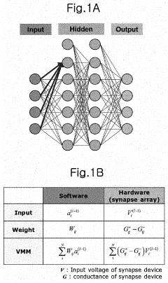
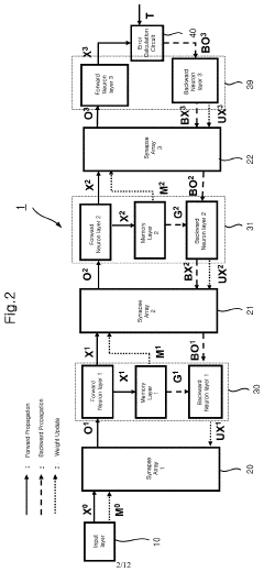
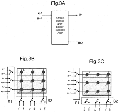
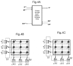
On-chip training neuromorphic architecture
PatentActiveUS20210232900A1
Innovation
- A neuromorphic architecture utilizing synapse arrays with gated Schottky diodes or nonvolatile memory devices, which perform all phases of neural network operations (forward propagation, backward propagation, and weighted value update) using small-sized, low-power-consumption circuits, minimizing memory and area usage.
Neuromorphic device
PatentPendingUS20220230060A1
Innovation
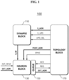
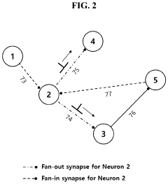
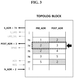
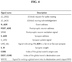
- A neuromorphic device employing a lookup table-based reconfigurable neural network architecture using the Address Event Representation (AER) method, which enables parallel search across divided partitions for high-speed spike routing and synapse weight updates through a topology block unit with parallel LUT modules, index address generation, and a comparator for efficient synaptic connection management.
Materials Science Innovations for Neuromorphic Computing
Materials science innovations are driving a revolution in neuromorphic computing, offering pathways to overcome the efficiency limitations of traditional von Neumann architectures. Novel materials with unique electrical, magnetic, and optical properties are enabling the development of brain-inspired computing systems that can process information with unprecedented energy efficiency and speed.
Memristive materials represent one of the most promising frontiers in this field. These materials, including metal oxides like HfO2, TiO2, and Ta2O5, exhibit non-volatile resistance changes based on their history of applied voltage or current. This property closely mimics biological synapses, making them ideal building blocks for neuromorphic systems. Recent advancements in controlling the stoichiometry and defect engineering of these oxides have significantly improved their switching reliability and endurance.
Phase-change materials (PCMs) offer another compelling approach for neuromorphic hardware implementation. Materials such as Ge2Sb2Te5 (GST) undergo rapid and reversible transitions between amorphous and crystalline states, enabling multi-level resistance states that can represent synaptic weights. Researchers have recently demonstrated PCM-based neuromorphic arrays capable of accelerating neural network training while consuming orders of magnitude less energy than conventional digital implementations.
Ferroelectric materials are emerging as candidates for ultra-low power neuromorphic computing. Materials like HfZrO2 and doped HfO2 exhibit polarization switching that can be leveraged for non-volatile memory and synaptic functions. Their CMOS compatibility makes them particularly attractive for large-scale integration with existing semiconductor manufacturing processes.
Two-dimensional materials, including graphene, MoS2, and hexagonal boron nitride, are enabling new device architectures for neuromorphic computing. Their atomically thin nature allows for vertical heterostructures with unique electronic properties. Recent demonstrations of artificial synapses based on 2D materials have shown exceptional performance metrics, including sub-picojoule energy consumption per synaptic event and nanosecond response times.
Spintronic materials, which leverage electron spin rather than charge, offer another promising direction. Magnetic tunnel junctions and spin-orbit torque devices can implement both memory and computational functions, potentially enabling true in-memory computing paradigms. These materials could lead to neuromorphic systems with significantly reduced energy consumption compared to CMOS-based implementations.
The convergence of these materials innovations with advanced fabrication techniques is accelerating the development of neuromorphic hardware that can approach the energy efficiency of biological brains while maintaining the speed advantages of electronic systems.
Standardization and Benchmarking Challenges
The standardization and benchmarking of neuromorphic chips represent significant challenges in advancing this technology toward widespread adoption. Currently, the field lacks universally accepted metrics for evaluating the performance, efficiency, and capabilities of different neuromorphic architectures. This fragmentation creates barriers for researchers, developers, and potential commercial adopters who struggle to make meaningful comparisons between competing solutions.
One primary challenge is the absence of standardized benchmarks specifically designed for neuromorphic computing. Traditional computing benchmarks focus on metrics like FLOPS or memory bandwidth, which fail to capture the unique characteristics of brain-inspired computing systems. Neuromorphic chips operate on fundamentally different principles, emphasizing spike-based processing, temporal dynamics, and distributed memory-processing architectures that conventional benchmarks cannot adequately assess.
The diversity of neuromorphic architectures further complicates standardization efforts. Different implementations vary significantly in their neural models, learning mechanisms, and hardware substrates—ranging from digital CMOS to analog, memristive, and photonic technologies. This heterogeneity makes it difficult to establish common evaluation frameworks that remain fair and relevant across the entire spectrum of neuromorphic approaches.
Energy efficiency metrics present another standardization challenge. While neuromorphic chips are inherently designed for improved energy efficiency, there is no consensus on how to measure this advantage in relation to specific computational tasks. Metrics must account for both static and dynamic power consumption patterns that differ substantially from conventional computing paradigms.
Application-specific performance evaluation adds another layer of complexity. Neuromorphic chips excel at certain tasks (pattern recognition, sensory processing) while potentially underperforming in others. Developing benchmarks that reflect real-world application scenarios rather than abstract computational capabilities remains an ongoing challenge.
The research community has begun addressing these issues through initiatives like the Neuromorphic Computing Benchmark (NCB) and the SNN Architecture Benchmark Suite, but these efforts remain in early stages. Industry participation in standardization processes has been limited, creating a disconnect between academic research metrics and commercial viability assessments.
Establishing trusted benchmarking methodologies will be crucial for accelerating innovation in neuromorphic computing. Standardized evaluation frameworks would enable fair comparison between different approaches, guide investment decisions, and help identify the most promising paths toward improved efficiency in smart neuromorphic chips.
Unlock deeper insights with PatSnap Eureka Quick Research — get a full tech report to explore trends and direct your research. Try now!
Generate Your Research Report Instantly with AI Agent
Supercharge your innovation with PatSnap Eureka AI Agent Platform!