

Comparing EUV Lithography Material Innovations Across Industries
OCT 14, 20259 MIN READ
Generate Your Research Report Instantly with AI Agent
PatSnap Eureka helps you evaluate technical feasibility & market potential.
EUV Lithography Evolution and Objectives
Extreme Ultraviolet (EUV) lithography represents a revolutionary advancement in semiconductor manufacturing, emerging after decades of research to overcome the physical limitations of traditional optical lithography. The technology's development began in the 1980s, with significant breakthroughs occurring in the late 1990s through collaborative industry efforts. EUV lithography utilizes 13.5nm wavelength light, enabling the production of semiconductor devices with feature sizes below 7nm, a critical threshold for continuing Moore's Law progression.
The evolution of EUV technology has been marked by several key milestones. Initially, researchers focused on developing reliable EUV light sources powerful enough for commercial applications. This was followed by breakthroughs in mirror technology, as traditional lenses absorb EUV radiation. The development of specialized photoresist materials capable of responding to EUV wavelengths represented another crucial advancement, with ongoing innovations continuing to enhance resolution and sensitivity.
Industry adoption has accelerated since 2018, when ASML delivered the first commercial EUV lithography systems. The technology has since become essential for manufacturing advanced logic chips at 7nm nodes and below. Current objectives focus on increasing throughput, reducing defectivity, and enhancing overall system reliability to support high-volume manufacturing environments.
Material innovations across industries have significantly contributed to EUV advancement. The semiconductor industry has pioneered specialized photoresists with improved sensitivity and resolution. Meanwhile, the optics industry has developed multi-layer mirrors with unprecedented reflectivity at EUV wavelengths. The chemical industry has created novel cleaning solutions to address contamination challenges unique to EUV processes.
Looking forward, EUV lithography aims to enable production at the 3nm node and beyond, requiring continued material innovations. Key objectives include developing photoresists with higher sensitivity to reduce exposure times, creating more durable mask materials to withstand intense EUV radiation, and formulating specialized cleaning chemistries to maintain pristine optical surfaces.
Cross-industry collaboration remains essential, with semiconductor manufacturers, equipment suppliers, material scientists, and research institutions working together to overcome remaining technical challenges. The ultimate goal is to establish EUV lithography as a stable, cost-effective manufacturing technology capable of supporting the next decade of semiconductor advancement, enabling continued miniaturization and performance improvements across computing platforms.
Market Demand Analysis for EUV Materials
The global market for Extreme Ultraviolet (EUV) lithography materials has witnessed exponential growth in recent years, primarily driven by the semiconductor industry's relentless pursuit of Moore's Law. Current market assessments value the EUV materials sector at approximately $2.5 billion in 2023, with projections indicating a compound annual growth rate (CAGR) of 17-20% through 2030, potentially reaching $8.7 billion by the end of the decade.
Semiconductor manufacturing represents the dominant application segment, accounting for over 85% of the total EUV materials market. This demand is fueled by leading chip manufacturers like TSMC, Samsung, and Intel, who are aggressively transitioning to EUV technology for their advanced node processes (5nm and below). Industry reports indicate that EUV adoption has accelerated faster than initially anticipated, with major fabs increasing their EUV equipment purchases by 35% year-over-year in 2022-2023.
Beyond semiconductors, emerging applications in advanced display manufacturing, particularly for high-resolution micro-LED displays, are creating new demand vectors for specialized EUV materials. This segment, though currently representing less than 5% of the market, is expected to grow at a CAGR of 25% through 2028 as display technologies continue to evolve toward higher pixel densities.
Regional analysis reveals Asia-Pacific dominates the demand landscape, accounting for approximately 70% of global EUV material consumption, with South Korea, Taiwan, and increasingly China being the primary markets. North America and Europe collectively represent about 28% of the market, with particular strength in research-intensive applications and specialty materials development.
The photoresist segment constitutes the largest material category, representing approximately 45% of the EUV materials market. Particularly, chemically amplified resists (CARs) and metal-oxide resists are experiencing heightened demand due to their enhanced resolution capabilities and sensitivity profiles. Pellicles and mask blanks follow as the second largest segment at 30%, with mask absorbers and other auxiliary materials comprising the remainder.
Supply chain constraints remain a significant market challenge, with over 60% of specialized EUV materials being produced by a small number of suppliers. This concentration has led to periodic shortages, particularly for advanced photoresists and mask blanks, driving prices upward by 15-20% in 2022-2023. Industry surveys indicate that 78% of semiconductor manufacturers consider EUV material availability a critical factor in their production planning.
Customer requirements are evolving rapidly, with increasing emphasis on materials that enable higher resolution (sub-10nm features), reduced defectivity (below 0.1 defects/cm²), and improved throughput compatibility. Additionally, sustainability considerations are emerging as a secondary but growing demand driver, with 40% of major semiconductor manufacturers now including environmental impact assessments in their material qualification processes.
Current EUV Material Challenges
Despite significant advancements in EUV lithography technology, several critical material challenges persist across the semiconductor manufacturing ecosystem. The photoresist materials currently used in EUV processes face fundamental limitations in sensitivity, resolution, and line edge roughness (LER) - creating what industry experts call the "triangle trade-off" where improving one parameter typically degrades the others. Chemically amplified resists (CARs), while offering high sensitivity, struggle with pattern collapse at sub-7nm nodes due to their inherent acid diffusion characteristics.
Metal-oxide resists have emerged as promising alternatives, particularly those incorporating hafnium and zirconium, but they continue to face integration challenges with existing manufacturing processes. The stochastic effects at extreme dimensions remain particularly problematic, causing random defects that significantly impact yield rates as feature sizes approach atomic scales.
Pellicle materials represent another critical challenge area. These thin membranes must withstand intense EUV radiation while maintaining transparency and thermal stability. Current silicon-based and polysilicon pellicles experience degradation under prolonged exposure, limiting their practical lifetime in high-volume manufacturing environments. The industry has yet to develop pellicle materials that can consistently survive the full lifetime requirements of high-volume manufacturing without significant transmission loss.
Mask absorber materials present their own set of challenges. Traditional tantalum-based absorbers suffer from mask 3D effects that create imaging artifacts as pattern dimensions shrink. While high-k materials show promise in reducing these effects, they introduce new integration complexities and potential defectivity issues that must be addressed before widespread adoption.
Underlying substrate materials also face limitations. The flatness requirements for EUV substrates are extraordinarily demanding, with specifications now in the picometer range. Current manufacturing capabilities struggle to consistently achieve these tolerances at economically viable yields.
Contamination control presents perhaps the most pervasive challenge across all EUV material systems. Carbon contamination from residual hydrocarbons in vacuum systems leads to reflectivity degradation in optical components. Tin debris from plasma sources requires sophisticated collection and mitigation strategies to prevent damage to sensitive optical surfaces.
Cross-industry collaboration has accelerated in addressing these challenges, with materials suppliers, equipment manufacturers, and semiconductor companies forming consortia to develop next-generation EUV materials. However, the fundamental physics limitations at these dimensions mean that material innovation must increasingly rely on atomic-level engineering approaches rather than incremental improvements to existing formulations.
Current EUV Resist and Mask Solutions
01 Photoresist materials for EUV lithography
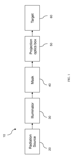
Specialized photoresist materials are essential for EUV lithography to achieve high resolution patterning. These materials are designed to be sensitive to extreme ultraviolet radiation (13.5 nm wavelength) and provide excellent pattern transfer capabilities. Advanced photoresist formulations include chemical amplification mechanisms, acid generators, and quenchers to control diffusion. The composition of these materials is critical for achieving the nanometer-scale features required in modern semiconductor manufacturing.- Photoresist materials for EUV lithography: Specialized photoresist materials are essential for EUV lithography processes. These materials are designed to be sensitive to extreme ultraviolet radiation and provide high resolution patterning capabilities. Advanced photoresist formulations include chemical amplification mechanisms that enhance sensitivity while maintaining pattern fidelity at nanometer scales. These materials often incorporate specific polymers and photoacid generators optimized for EUV wavelengths.
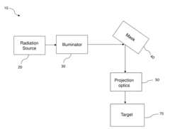
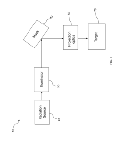
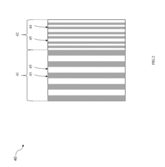
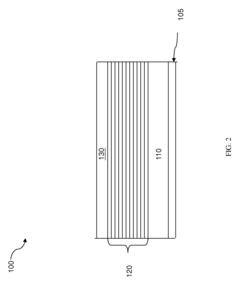
- Reflective optics and multilayer mirrors: EUV lithography systems utilize specialized reflective optics and multilayer mirrors instead of traditional transmissive optics due to the high absorption of EUV radiation by most materials. These mirrors typically consist of alternating layers of materials with high EUV reflectivity, such as molybdenum and silicon. The precise thickness and composition of these multilayer structures are critical for achieving high reflectivity at the 13.5 nm EUV wavelength while maintaining thermal stability under intense radiation.
- Pellicle materials for EUV mask protection: Pellicles serve as protective membranes for EUV photomasks, preventing contamination while allowing EUV radiation to pass through with minimal absorption. These materials must be extremely thin (typically a few nanometers) yet mechanically robust, with high thermal stability and resistance to radiation damage. Advanced pellicle materials include silicon-based compounds, carbon-based materials like graphene, and metal-doped thin films that can withstand the intense conditions of EUV exposure while maintaining optical performance.
- EUV source materials and plasma generation: EUV radiation sources typically utilize tin, xenon, or lithium-based materials that are excited to generate plasma emitting at the required 13.5 nm wavelength. These materials are delivered as droplets, jets, or thin films and are excited by high-power lasers or electrical discharges. The choice of source material affects critical parameters such as conversion efficiency, debris generation, and spectral purity. Advanced source designs incorporate sophisticated debris mitigation systems and optimized material delivery mechanisms to enhance reliability and extend component lifetimes.
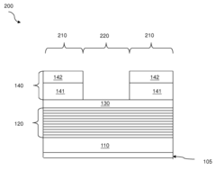
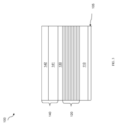
- Mask materials and absorber layers: EUV masks consist of multilayer reflective substrates with patterned absorber layers that define the circuit features. The absorber materials must provide high contrast between reflective and absorbing regions while maintaining pattern accuracy at extremely small dimensions. Common absorber materials include tantalum-based compounds and other high-atomic-number elements that efficiently absorb EUV radiation. The mask substrate requires exceptional flatness and thermal stability to prevent pattern distortion during the high-energy exposure process.
02 Reflective optical elements and multilayer mirrors
EUV lithography systems rely on reflective optics rather than traditional transmissive lenses due to the high absorption of EUV radiation in most materials. Multilayer mirrors consisting of alternating layers of materials with different refractive indices (typically molybdenum and silicon) are used to reflect EUV radiation with high efficiency. These mirrors require precise engineering to maintain reflectivity and withstand the intense radiation environment without degradation over time.Expand Specific Solutions03 Pellicle materials for EUV mask protection
Pellicles are thin membranes used to protect photomasks from contamination in lithography processes. For EUV lithography, specialized pellicle materials must be extremely thin while maintaining mechanical stability and high transmittance at the 13.5 nm wavelength. These materials often include silicon-based compounds, carbon nanomaterials, or metal films with engineered thickness. The pellicle must withstand high-intensity EUV radiation without degradation while preventing particles from reaching the mask surface.Expand Specific Solutions04 EUV mask materials and absorber layers
EUV masks consist of a multilayer reflective stack with patterned absorber materials on top. The absorber materials must provide high contrast by efficiently absorbing EUV radiation while being thin enough for high-resolution patterning. Common absorber materials include tantalum-based compounds, which offer good absorption properties and etching selectivity. The mask substrate and buffer layers must maintain flatness and thermal stability during the manufacturing process and exposure to intense EUV radiation.Expand Specific Solutions05 Contamination control materials and cleaning solutions
EUV lithography systems are highly sensitive to contamination, requiring specialized materials for contamination control. These include carbon trap materials to capture hydrocarbon contaminants, hydrogen gas systems to prevent oxidation of optical surfaces, and specialized cleaning solutions that can remove residues without damaging delicate optical components. Advanced filtration systems and materials are also employed to maintain the ultra-clean environment required for EUV lithography processes.Expand Specific Solutions
Leading EUV Material Suppliers and Manufacturers
The EUV lithography materials market is in a growth phase, characterized by rapid technological advancements and increasing adoption across semiconductor manufacturing. The global market size is expanding significantly as chipmakers transition to more advanced nodes, with projections indicating substantial growth through 2030. Technologically, industry leaders like ASML, which dominates EUV lithography equipment manufacturing, are driving innovation alongside materials specialists. Taiwan Semiconductor Manufacturing Co. leads implementation, while companies like AGC, Shin-Etsu Chemical, and Tokyo Electron are advancing critical materials development. Research institutions including Chinese Academy of Sciences and Korea Electronics Technology Institute collaborate with industry players like Samsung SDI and GLOBALFOUNDRIES to overcome technical challenges in resist materials, pellicles, and mask technologies. The competitive landscape features established semiconductor giants and specialized materials providers working to address EUV's unique requirements for next-generation chip production.
Taiwan Semiconductor Manufacturing Co., Ltd.
Technical Solution: TSMC has pioneered the implementation of EUV lithography in high-volume manufacturing, developing specialized material formulations optimized for their specific process flows. Their approach focuses on metal-oxide EUV resists with tailored sensitizers that enhance sensitivity while maintaining resolution and line edge roughness performance. TSMC has created proprietary underlayer materials that improve adhesion and reduce pattern collapse in ultra-fine features. Their EUV process integrates specialized development chemistries that enhance contrast and reduce defectivity. TSMC's material innovation extends to specialized cleaning solutions that remove residual contamination without damaging delicate nanostructures. Their EUV implementation includes customized hard mask materials with exceptional etch selectivity for pattern transfer into diverse substrate materials. TSMC's material ecosystem is designed for compatibility across multiple device generations, enabling technology roadmap extension.
Strengths: Extensive practical manufacturing experience with EUV materials; ability to optimize material formulations for specific device requirements; vertical integration of material development with process engineering. Weaknesses: Heavy dependence on external material suppliers for base components; materials optimized specifically for TSMC's process flows may not transfer to other manufacturers.
SAMSUNG SDI CO LTD
Technical Solution: Samsung SDI has developed advanced EUV photoresist materials with metal-organic frameworks that provide enhanced sensitivity and reduced line edge roughness. Their hybrid resist systems incorporate specialized nanoparticles that improve absorption at 13.5nm wavelength while maintaining high resolution capability. Samsung's material innovation includes development of low-outgassing topcoat materials that protect the resist during exposure and development processes. They have pioneered multi-trigger resist chemistries that require lower exposure doses, addressing one of EUV's key challenges. Samsung SDI's material portfolio includes specialized rinse solutions that prevent pattern collapse in high-aspect-ratio features. Their EUV-specific anti-reflective coating materials minimize reflectivity and standing wave effects unique to EUV wavelengths. Samsung has also developed specialized developer solutions with controlled diffusion properties to enhance contrast in EUV imaging.
Strengths: Vertical integration with Samsung Electronics provides direct manufacturing feedback; strong chemical engineering capabilities; extensive testing infrastructure for material qualification. Weaknesses: Materials primarily optimized for Samsung's internal processes; relatively newer entrant to commercial EUV material supply compared to established chemical companies.
Key EUV Material Patents and Innovations
Extreme Ultraviolet Lithography Process and Mask
PatentActiveUS20150168845A1
Innovation
- The implementation of a nearly on-axis illumination with partial coherence less than 0.3 in an EUV lithography system, combined with an EUV mask featuring a first region with main polygons and a second region with sub-resolution polygons, and a spatial filter to remove most non-diffracted light, enhancing spatial frequency resolution and uniformity of exposure intensity.
Extreme ultraviolet lithography process and mask
PatentActiveUS9448491B2
Innovation
- A mask structure incorporating a reflective multilayer with a flare-suppressing absorption stack (FSAS) and a flare-suppressing-by-phase-shifting (FSbPhS) layer, which absorbs EUV light and induces destructive interference to suppress OOB radiation, specifically DUV flare, enhancing image contrast and lithography performance.
Cross-Industry Applications of EUV Technology
Extreme Ultraviolet (EUV) lithography technology has demonstrated remarkable versatility across multiple industries beyond its primary application in semiconductor manufacturing. The semiconductor industry remains the primary adopter, utilizing EUV lithography to achieve sub-7nm node fabrication capabilities essential for advanced microprocessors and memory devices. Leading companies like TSMC, Samsung, and Intel have invested billions in EUV infrastructure to maintain competitive advantages in chip production.
The medical device industry has begun leveraging EUV technology for manufacturing high-precision components for diagnostic equipment and implantable devices. The nanometer-scale resolution enables the creation of microfluidic channels for lab-on-chip applications and intricate patterns for biosensors with unprecedented sensitivity. Companies like Medtronic and Siemens Healthineers are exploring EUV-based manufacturing for next-generation medical technologies.
Aerospace and defense sectors utilize EUV lithography for developing advanced radar systems, optical sensors, and communication equipment requiring nanoscale precision. The technology enables the production of high-frequency components with improved signal processing capabilities and reduced power consumption. Lockheed Martin and Raytheon have established research programs specifically focused on EUV applications for military-grade electronics.
In the automotive industry, EUV technology supports the development of advanced driver-assistance systems (ADAS) and autonomous vehicle sensors. The high-resolution patterning capabilities facilitate the production of more efficient LiDAR components and image sensors critical for environmental perception. Companies like Bosch and Continental are incorporating EUV-manufactured components into their next-generation automotive electronics.
The telecommunications sector has adopted EUV lithography for creating advanced photonic integrated circuits essential for 5G and future 6G infrastructure. These components enable higher data transmission rates with lower latency and improved energy efficiency. Huawei, Nokia, and Ericsson have all invested in EUV-related research to enhance their telecommunications hardware offerings.
Quantum computing represents an emerging application area, where EUV lithography enables the fabrication of quantum bits (qubits) with precise dimensions and spacing. This precision is crucial for maintaining quantum coherence and reducing error rates in quantum processors. IBM, Google, and Intel are utilizing EUV technology in their quantum computing research programs to overcome current fabrication limitations.
Environmental Impact of EUV Materials
The environmental footprint of Extreme Ultraviolet (EUV) lithography materials represents a critical consideration as semiconductor manufacturing advances. These specialized materials, including photoresists, pellicles, and mask blanks, contain various chemical compounds that pose significant environmental challenges throughout their lifecycle. The production of EUV materials typically involves energy-intensive processes and hazardous chemicals such as perfluorinated compounds, heavy metals, and various solvents that can persist in the environment.
Manufacturing facilities utilizing EUV lithography generate substantial waste streams that require specialized treatment. Photoresist materials, particularly those containing metal-organic compounds for EUV sensitivity, create complex waste management challenges due to their unique chemical properties. Industry data indicates that a typical semiconductor fabrication plant may produce between 5,000-7,000 metric tons of chemical waste annually, with EUV-related materials comprising an increasing percentage as adoption grows.
Water consumption represents another significant environmental concern. The purification processes for EUV materials require ultra-pure water in substantial quantities, with estimates suggesting that advanced semiconductor manufacturing facilities consume between 2-4 million gallons daily. This intensive water usage occurs in an industry increasingly concentrated in regions facing water scarcity challenges, creating potential sustainability conflicts.
Energy consumption associated with EUV material production and usage cannot be overlooked. The specialized manufacturing environments required for these materials demand precise temperature and humidity controls, clean room facilities, and energy-intensive purification processes. Current industry assessments indicate that EUV lithography systems consume approximately 40% more energy than previous generation deep ultraviolet (DUV) systems, partly due to the specialized material requirements.
Cross-industry comparisons reveal varying approaches to environmental mitigation. The semiconductor industry has implemented more advanced recycling programs for EUV materials than adjacent industries utilizing similar compounds. For instance, recovery rates for precious metals from EUV photoresists exceed 85% in leading semiconductor facilities, compared to approximately 60% in other precision manufacturing sectors.
Regulatory frameworks governing EUV materials differ significantly across regions, with the European Union's REACH regulations imposing the strictest controls on perfluorinated compounds commonly used in EUV processes. This regulatory divergence has accelerated innovation in environmentally preferable alternatives, particularly among European material suppliers who have pioneered bio-based photoresist components that reduce environmental persistence while maintaining performance specifications.
Unlock deeper insights with PatSnap Eureka Quick Research — get a full tech report to explore trends and direct your research. Try now!
Generate Your Research Report Instantly with AI Agent
Supercharge your innovation with PatSnap Eureka AI Agent Platform!