EUV Lithography: Innovations in Light Source and Exposure Technology
OCT 14, 20259 MIN READ
Generate Your Research Report Instantly with AI Agent
Patsnap Eureka helps you evaluate technical feasibility & market potential.
EUV Lithography Evolution and Objectives
Extreme Ultraviolet (EUV) lithography represents a revolutionary advancement in semiconductor manufacturing technology, marking a significant departure from traditional optical lithography methods. The evolution of EUV lithography began in the late 1980s when semiconductor industry leaders recognized the limitations of conventional deep ultraviolet (DUV) lithography in achieving smaller feature sizes. The fundamental shift involved moving from 193nm wavelength light sources to 13.5nm EUV light, enabling the production of significantly smaller transistors and more densely packed integrated circuits.
Throughout the 1990s, research consortia including ASML, Intel, and IBM invested heavily in developing viable EUV technology, though progress was initially slow due to formidable technical challenges. The early 2000s saw critical breakthroughs in source power technology, with the development of laser-produced plasma (LPP) sources using tin droplets as the primary approach. By 2010, the industry had largely converged on this solution, though source power remained insufficient for high-volume manufacturing.
The period from 2010 to 2020 witnessed dramatic improvements in EUV source power, from less than 10W to over 250W, finally enabling commercial viability. ASML delivered its first production-ready EUV systems in 2017, with Samsung and TSMC implementing the technology in their 7nm and 5nm process nodes shortly thereafter. This transition represented the most significant lithography advancement in decades, overcoming what many had considered an insurmountable barrier to continued semiconductor scaling.
The primary objective of EUV lithography development has been to extend Moore's Law by enabling continued miniaturization of semiconductor devices. Specific technical goals include achieving resolution below 10nm, increasing wafer throughput to economically viable levels (currently targeting >125 wafers per hour), and improving overlay accuracy to below 1.5nm to ensure precise pattern alignment across multiple layers.
Current research focuses on enhancing EUV source brightness and stability, developing more sensitive photoresists with reduced line edge roughness, and improving mask infrastructure to reduce defects. High-numerical aperture (High-NA) EUV systems represent the next evolutionary step, promising to extend resolution capabilities to the 3nm node and beyond through increased light collection efficiency.
The industry roadmap envisions EUV lithography remaining the dominant advanced patterning technology through at least 2030, with continuous improvements in resolution, throughput, and cost-effectiveness. Beyond this horizon, complementary technologies such as directed self-assembly and next-generation EUV sources may emerge to further extend semiconductor scaling capabilities.
Semiconductor Industry Demand Analysis
The semiconductor industry's demand for advanced lithography technologies, particularly EUV (Extreme Ultraviolet) lithography, is primarily driven by the relentless pursuit of Moore's Law. As transistor dimensions continue to shrink below 10nm, traditional DUV (Deep Ultraviolet) lithography has reached its physical limits, creating an urgent need for EUV technology to enable further miniaturization.
Market analysis indicates that the global semiconductor equipment market is experiencing robust growth, with lithography systems representing one of the largest segments. The EUV lithography equipment market specifically is projected to grow significantly through 2030, as chipmakers transition to more advanced nodes. This growth is fueled by increasing demand for high-performance computing, artificial intelligence, 5G infrastructure, and autonomous vehicles - all requiring chips with greater transistor density and computational power.
Leading semiconductor manufacturers including TSMC, Samsung, and Intel have committed substantial investments to EUV technology adoption. TSMC alone has ordered multiple EUV systems for its advanced manufacturing processes at 5nm and below. This industry-wide transition represents a multi-billion dollar market opportunity for EUV lithography equipment and related technologies.
The demand for EUV lithography is particularly strong in memory chip production, where manufacturers seek to increase storage density while reducing power consumption. DRAM and NAND flash memory producers are gradually incorporating EUV processes to achieve competitive advantages in both performance and cost metrics.
Geographic analysis reveals concentrated demand in East Asia, particularly Taiwan, South Korea, and increasingly China, where the majority of semiconductor manufacturing occurs. However, recent geopolitical developments have accelerated plans for semiconductor manufacturing expansion in the United States and Europe, potentially broadening the market for advanced lithography equipment.
Industry forecasts suggest that EUV lithography will remain critical for at least the next decade, with the potential market expanding as the technology becomes more accessible to a broader range of semiconductor manufacturers. Currently, the high cost of EUV systems (approximately $150 million per tool) limits adoption to only the largest manufacturers, but ongoing innovations in light source efficiency and exposure technology could eventually reduce costs and expand market penetration.
The semiconductor industry's cyclical nature affects demand patterns, but the strategic importance of maintaining technological leadership ensures continued investment in advanced lithography capabilities even during market downturns. This creates a relatively stable long-term demand trajectory for EUV lithography innovations, particularly those addressing current limitations in throughput, reliability, and cost-effectiveness.
EUV Technical Barriers and Global Development Status
EUV lithography technology currently faces several significant technical barriers that have shaped its global development trajectory. The most fundamental challenge remains the light source technology, where achieving sufficient power output for high-volume manufacturing continues to be problematic. Current EUV systems operate at 13.5nm wavelength using laser-produced plasma sources, but maintaining stable, high-power output above 250W has proven difficult, limiting throughput in production environments.
Mask defectivity presents another critical barrier, as EUV masks require near-perfect surfaces due to the reflective nature of the technology. Even nanometer-scale defects can cause significant pattern distortions, and inspection tools capable of detecting these defects remain limited in capability and availability. This has created bottlenecks in the mask qualification process.
Photoresist technology specifically designed for EUV presents ongoing challenges. The fundamental physics of EUV exposure differs from traditional lithography, requiring resists that can achieve high resolution with fewer photons. Current resists struggle with the sensitivity-resolution-line edge roughness trade-off, necessitating continued innovation in resist chemistry.
From a global development perspective, EUV technology has become increasingly concentrated in specific geographic regions. The Netherlands dominates equipment manufacturing through ASML's monopoly on EUV scanners, while Japan leads in mask blanks and related materials. The United States maintains strength in light source technology and system integration, and South Korea has become a leader in actual implementation of EUV in high-volume manufacturing.
China's access to EUV technology has been severely restricted by export controls, creating a significant technological divide in semiconductor manufacturing capabilities globally. This geopolitical dimension has accelerated domestic development efforts in alternative lithography approaches in affected regions.
The economic barriers to EUV adoption remain substantial, with each exposure tool costing approximately $150-200 million, plus significant infrastructure requirements. This has limited adoption to only the largest semiconductor manufacturers, primarily in Taiwan, South Korea, and the United States, creating a stratification in the global semiconductor industry between those with and without access to leading-edge lithography.
Technical progress has been steady but slower than initially projected, with each power and resolution milestone taking longer to achieve than industry roadmaps anticipated. This has necessitated continued reliance on multiple patterning techniques even with EUV implementation, adding complexity to the manufacturing process.
Current EUV Light Source and Exposure Solutions
01 EUV light source technology
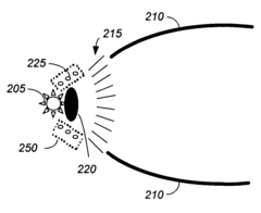
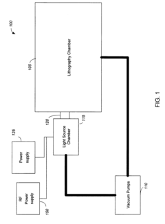
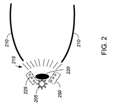
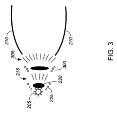
Extreme Ultraviolet (EUV) lithography requires specialized light sources that can generate radiation at extremely short wavelengths, typically around 13.5nm. These light sources often involve laser-produced plasma or discharge-produced plasma technologies where high-energy lasers or electrical discharges strike targets (often tin droplets) to create the EUV radiation. The technology includes sophisticated systems for droplet generation, laser pulse timing, and plasma containment to maximize EUV output while minimizing debris that could contaminate optical components.- EUV light source technology: Extreme Ultraviolet (EUV) lithography requires specialized light sources that can generate radiation at extremely short wavelengths. These light sources typically involve plasma generation systems that produce EUV radiation at 13.5nm wavelength. The technology includes various approaches such as laser-produced plasma (LPP) or discharge-produced plasma (DPP) sources, along with collector optics to efficiently capture and direct the EUV radiation. Innovations in this area focus on increasing source power, stability, and reliability to meet the demanding requirements of high-volume semiconductor manufacturing.
- EUV exposure system architecture: EUV lithography exposure systems employ a complex architecture of optical components designed to work with extreme ultraviolet wavelengths. These systems typically include reflective optics rather than traditional transmissive lenses, utilizing multilayer mirrors with specialized coatings to reflect EUV radiation. The architecture encompasses illumination systems, projection optics, and precise positioning stages that work together to achieve nanometer-scale resolution. Innovations focus on system integration, minimizing aberrations, and maintaining optical performance under vacuum conditions required for EUV operation.
- EUV mask technology and handling: EUV lithography requires specialized photomasks with reflective multilayer coatings rather than traditional transmissive masks. These masks incorporate absorber patterns on reflective substrates and require protection from contamination and damage. Innovations in this area include defect inspection and repair techniques, handling systems to prevent particulate contamination, and methods to compensate for mask defects during exposure. Advanced mask technologies also address issues related to pattern fidelity, three-dimensional mask effects, and compatibility with increasingly smaller feature sizes.
- EUV process control and optimization: EUV lithography requires sophisticated process control methods to achieve consistent results at extreme resolutions. This includes techniques for optimizing dose control, focus, overlay accuracy, and critical dimension uniformity. Advanced computational methods are employed for optical proximity correction, source mask optimization, and process window enhancement. The technology also encompasses metrology systems for in-situ monitoring and feedback control to maintain process stability despite the challenges of working with EUV wavelengths in vacuum environments.
- EUV system contamination control: Contamination control is critical in EUV lithography systems due to their operation in vacuum environments and sensitivity to molecular and particulate contamination. Technologies in this area include specialized vacuum systems, hydrogen gas curtains to prevent carbon contamination of optical surfaces, and cleaning methods for mirrors and other components. Innovations focus on extending the lifetime of optical components by mitigating contamination from resist outgassing, preventing tin debris from the EUV source from reaching sensitive optics, and maintaining the reflectivity of multilayer mirrors over extended operation periods.
02 Optical systems for EUV exposure
EUV lithography requires specialized optical systems due to the unique properties of extreme ultraviolet light. These systems typically employ reflective optics rather than refractive lenses since EUV radiation is absorbed by most materials. Multi-layer mirrors with alternating layers of materials provide the necessary reflectivity for EUV wavelengths. The optical path must be maintained in vacuum conditions to prevent absorption of the EUV radiation by air molecules. Advanced optical designs incorporate multiple mirrors arranged to minimize aberrations while maximizing the amount of EUV light reaching the wafer surface.Expand Specific Solutions03 Mask technology for EUV lithography
EUV lithography employs specialized reflective masks rather than the transmissive masks used in conventional optical lithography. These masks consist of a multilayer reflective coating on a substrate with an absorber pattern that defines the circuit features. The mask structure must maintain extreme precision to ensure accurate pattern transfer at the nanometer scale. Advanced mask technologies include phase-shifting elements and various techniques to enhance resolution and minimize defects. Mask inspection and repair technologies are critical due to the sensitivity of EUV processes to even nanometer-scale imperfections.Expand Specific Solutions04 EUV exposure control and alignment systems
Precise control of the exposure process is critical in EUV lithography due to the extremely small feature sizes being produced. Advanced systems incorporate sophisticated sensors and feedback mechanisms to control dose uniformity across the wafer. Alignment systems must achieve positioning accuracy in the sub-nanometer range to ensure proper overlay between multiple patterning layers. These systems often employ interferometric measurement techniques and complex algorithms to compensate for thermal expansion, mechanical vibration, and other factors that could affect alignment precision.Expand Specific Solutions05 Contamination control and system maintenance
EUV lithography systems require exceptional cleanliness due to the sensitivity of the process to particulate and molecular contamination. Advanced contamination control strategies include sophisticated vacuum systems, hydrogen cleaning processes, and specialized materials that minimize outgassing. Carbon contamination on optical surfaces is a particular concern as it can reduce reflectivity of the mirrors. Maintenance protocols include regular cleaning procedures and monitoring systems that can detect degradation in optical performance. The overall system design must balance performance requirements with practical considerations for maintenance access and component lifetime.Expand Specific Solutions
Leading EUV Equipment Manufacturers and Ecosystem
EUV Lithography is currently in a transitional growth phase, with the market expected to expand significantly from approximately $5 billion to over $10 billion by 2027. The technology has reached commercial maturity for leading-edge semiconductor manufacturing, though continuous innovation remains crucial. ASML dominates the equipment landscape with its NXE systems, while companies like Cymer and Gigaphoton compete in light source technology. Intel, Samsung, TSMC, and SK Hynix represent major adopters driving implementation. Supporting ecosystem players include Carl Zeiss SMT (optics), AGC and Shin-Etsu (mask blanks), and Hoya (photomask materials). Chinese entities like SMIC and Shanghai Micro Electronics Equipment are working to develop domestic capabilities, though they lag significantly behind the established leaders in this highly specialized field.
Nikon Corp.
Technical Solution: Nikon has developed a competitive approach to EUV lithography through its NSR-S635E system, which utilizes a discharge-produced plasma (DPP) light source rather than the laser-produced plasma approach favored by ASML. Their system architecture focuses on maximizing throughput while maintaining precision, achieving overlay accuracy of <1.5nm and critical dimension uniformity below 1.2nm. Nikon's EUV technology incorporates proprietary optical designs that minimize aberrations and maximize light collection efficiency. Their systems feature advanced wafer handling mechanisms that reduce non-exposure overhead time, increasing the effective throughput to over 100 wafers per hour for certain process steps. Nikon has also developed specialized resist processing techniques optimized for their exposure systems, working closely with material suppliers to enhance sensitivity while maintaining pattern fidelity. Their EUV platform integrates with Nikon's established lithography control software, providing seamless operation with existing DUV systems in mixed lithography environments.
Strengths: Extensive experience in optical systems and precision engineering; established relationships with semiconductor manufacturers; competitive pricing compared to ASML systems; strong service infrastructure. Weaknesses: Significantly smaller market share in EUV segment; less mature EUV technology ecosystem; lower system performance specifications compared to latest ASML offerings; limited deployment in leading-edge manufacturing.
ASML Netherlands BV
Technical Solution: ASML is the undisputed leader in EUV lithography, holding a virtual monopoly on EUV lithography systems. Their NXE platform represents the cutting edge of EUV technology, with the latest NXE:3600D system achieving resolution down to 13nm with a numerical aperture (NA) of 0.33. ASML's technology integrates sophisticated laser-produced plasma (LPP) light sources that generate 13.5nm wavelength light by firing CO2 lasers at tin droplets, creating high-energy plasma. Their systems incorporate advanced computational lithography, including optical proximity correction and source mask optimization to enhance pattern fidelity. ASML has pioneered innovations in EUV optics, including the development of multilayer mirrors with more than 100 alternating layers of molybdenum and silicon to achieve over 70% reflectivity at EUV wavelengths. Their systems feature sophisticated vacuum environments and contamination control systems to maintain optimal performance.
Strengths: Unmatched technical expertise in EUV systems integration; proprietary technology in critical subsystems; extensive patent portfolio; established ecosystem with chip manufacturers. Weaknesses: Extremely high system costs (>$150 million per tool); complex supply chain dependencies; limited production capacity causing delivery delays; systems require significant facility infrastructure and maintenance.
Critical Patents and Breakthroughs in EUV Technology
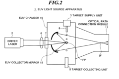
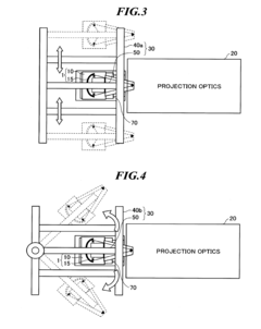
Plasma-based debris mitigation for extreme ultraviolet (EUV) light source
PatentInactiveUS7652272B2
Innovation
- The implementation of 'foil traps' and a secondary plasma to capture and ionize debris particles, combined with magnetic and electric forces to direct them away from collector mirrors, along with coatings and plasma source configurations to minimize sputtering and optimize gas flow, effectively mitigates plasma erosion.
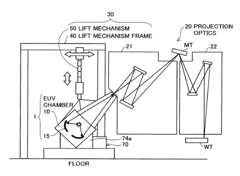
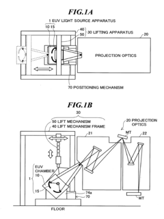
Extreme ultraviolet light source system
PatentInactiveUS20120119118A1
Innovation
- The integration of a lifting apparatus within the EUV light source system allows for easy replacement of heavy components by lifting and moving them, aligning the optical axis with the projection optics, thereby simplifying maintenance and reducing the effort required for part replacement.
Supply Chain Resilience for EUV Components
The EUV lithography supply chain represents one of the most complex and vulnerable technological ecosystems in the semiconductor industry. The highly specialized nature of EUV components creates significant resilience challenges, with many critical parts having single-source suppliers. ASML, as the sole manufacturer of EUV lithography systems, depends on a network of over 5,000 suppliers globally, with approximately 800 considered critical to operations.
Key vulnerabilities exist in the sourcing of specialized materials required for EUV components. The ultra-high purity materials needed for mirrors, masks, and light sources often come from geographically concentrated regions. For instance, specialized rare earth elements used in laser-produced plasma systems are predominantly sourced from China, creating geopolitical dependencies. Similarly, the specialized ceramics used in vacuum chambers come from a limited number of suppliers in Japan and Germany.
The COVID-19 pandemic exposed significant weaknesses in the EUV supply chain, with disruptions causing delays in system deliveries and impacting semiconductor manufacturing roadmaps globally. These disruptions highlighted the need for more robust contingency planning and alternative sourcing strategies for critical components.
Leading semiconductor manufacturers have begun implementing multi-faceted approaches to enhance supply chain resilience. Intel and TSMC have established strategic supplier diversification programs, investing in alternative suppliers for critical components where possible. Samsung has focused on vertical integration, bringing production of certain specialized components in-house to reduce external dependencies.
Geographical diversification represents another key strategy, with companies establishing redundant supply networks across different regions. This approach helps mitigate risks associated with natural disasters, geopolitical tensions, or regional health crises. ASML has expanded its supplier network across Europe, North America, and parts of Asia to reduce concentration risks.
Advanced inventory management systems utilizing AI-driven predictive analytics are being deployed to optimize stockpiling of critical components. These systems help balance the financial costs of carrying excess inventory against the operational risks of shortages. Additionally, digital twin technology is being employed to simulate supply chain disruptions and test mitigation strategies before implementation.
Industry consortia and public-private partnerships are emerging as collaborative approaches to supply chain resilience. The Semiconductor Supply Chain Initiative, involving major manufacturers, suppliers, and government entities, aims to coordinate efforts in addressing vulnerabilities and developing shared contingency plans for critical EUV components.
Environmental Impact and Energy Efficiency Considerations
EUV lithography represents a significant advancement in semiconductor manufacturing, but its environmental impact and energy efficiency considerations deserve careful examination. The technology's power-intensive nature presents substantial environmental challenges, with a single EUV system consuming approximately 1 MW of electricity during operation—significantly higher than previous lithography technologies. This increased energy demand contributes to higher carbon emissions when powered by non-renewable energy sources, raising concerns about the semiconductor industry's growing carbon footprint.
Water usage presents another environmental consideration, as EUV systems require extensive cooling systems that consume large volumes of ultra-pure water. A typical semiconductor fabrication facility using EUV technology may use millions of gallons of water daily, placing pressure on local water resources, particularly in water-stressed regions where many manufacturing facilities are located.
The production and operation of EUV systems also involve various specialized materials and gases, including rare earth elements for optics and xenon or tin for plasma generation. The extraction and processing of these materials can lead to habitat disruption, while the gases used may have high global warming potential if released into the atmosphere. Proper handling and disposal protocols are essential to minimize these impacts.
Industry leaders have recognized these challenges and implemented various efficiency improvements. ASML, the primary manufacturer of EUV systems, has developed more energy-efficient laser systems and optimized cooling technologies that reduce power consumption by up to 20% compared to earlier generations. Semiconductor manufacturers like TSMC and Samsung have invested in on-site renewable energy generation and water recycling systems, with some facilities achieving water reuse rates exceeding 85%.
Looking forward, several promising developments may further improve the environmental profile of EUV lithography. Research into alternative plasma generation methods could reduce energy requirements, while advanced cooling technologies using computational fluid dynamics are being developed to minimize water consumption. Additionally, the semiconductor industry's commitment to carbon neutrality is driving investment in energy-efficient facility design and renewable energy procurement.
Despite these challenges, it's important to consider that EUV lithography enables the production of more energy-efficient chips. The advanced processors manufactured using this technology typically consume less power per computation than previous generations, potentially offsetting some of the environmental impact of the manufacturing process through more efficient end products.
Unlock deeper insights with Patsnap Eureka Quick Research — get a full tech report to explore trends and direct your research. Try now!
Generate Your Research Report Instantly with AI Agent
Supercharge your innovation with Patsnap Eureka AI Agent Platform!