Exploring EUV Lithography's Potential in Medical Device Innovations
OCT 14, 20259 MIN READ
Generate Your Research Report Instantly with AI Agent
Patsnap Eureka helps you evaluate technical feasibility & market potential.
EUV Lithography Background and Medical Applications
Extreme Ultraviolet (EUV) lithography represents a revolutionary advancement in semiconductor manufacturing technology, operating at a wavelength of 13.5 nanometers. This technology emerged from decades of research aimed at overcoming the physical limitations of traditional optical lithography methods. Initially conceptualized in the 1980s, EUV lithography faced significant technical challenges including source power limitations, mask defects, and resist performance issues before reaching commercial viability in the late 2010s.
The evolution of EUV lithography has been driven by the semiconductor industry's relentless pursuit of Moore's Law, enabling the creation of increasingly smaller transistors and more powerful integrated circuits. ASML, in collaboration with research partners like IMEC and leading semiconductor manufacturers, has pioneered the development of EUV lithography systems that now serve as the cornerstone of advanced chip production below the 7nm node.
While primarily developed for semiconductor manufacturing, EUV lithography's unprecedented precision and resolution capabilities present compelling opportunities for medical device innovation. The ability to create nanoscale features with extreme accuracy opens new frontiers in medical technology development, particularly in areas requiring miniaturization and precision manufacturing.
In the medical field, EUV lithography could potentially revolutionize several critical application areas. For implantable medical devices, this technology enables the creation of microscale components with complex geometries and precise surface features that can enhance biocompatibility and functionality. Diagnostic platforms could benefit from EUV-enabled microfluidic systems with nanoscale channels for enhanced sensitivity in detecting biomarkers at previously undetectable concentrations.
Drug delivery systems represent another promising application area, where EUV lithography could facilitate the development of precisely engineered micro/nano-carriers with controlled release mechanisms. Additionally, neural interfaces and brain-computer interface technologies could leverage EUV's precision to create higher-density electrode arrays with improved biocompatibility profiles.
The technical objectives for adapting EUV lithography to medical applications include developing specialized resist materials compatible with biological applications, creating cost-effective manufacturing processes for medical-grade components, and establishing quality control protocols that meet stringent regulatory requirements for medical devices. Furthermore, research aims to explore how EUV-enabled nanopatterning can enhance surface properties to improve cell adhesion, reduce biofouling, and create antimicrobial surfaces.
As the technology continues to mature, the convergence of EUV lithography with medical device innovation promises to address critical healthcare challenges through unprecedented manufacturing capabilities at the nanoscale.
Market Analysis for EUV-Enabled Medical Devices
The global market for medical devices enabled by Extreme Ultraviolet (EUV) lithography technology is poised for significant growth over the coming decade. Current market assessments indicate that the precision medical device sector, which stands to benefit most from EUV advancements, is valued at approximately $85 billion globally, with annual growth rates consistently exceeding 6% since 2018.
EUV lithography's potential to create nanoscale features with unprecedented precision opens new market segments within the medical device industry. Implantable medical devices represent the largest potential market segment, with particular emphasis on neural interfaces, smart drug delivery systems, and miniaturized diagnostic tools. The neural interface market alone is projected to grow at a compound annual growth rate of 15.2% through 2030.
Geographical distribution of market demand shows North America currently leading with 42% market share, followed by Europe (28%), Asia-Pacific (24%), and rest of world (6%). However, the Asia-Pacific region demonstrates the fastest growth trajectory, particularly in Japan, South Korea, and Singapore, where significant investments in advanced medical technologies are being made.
Reimbursement policies and regulatory frameworks significantly influence market adoption rates. Markets with favorable reimbursement structures for innovative medical technologies, such as Germany and the United States, show accelerated adoption curves for precision medical devices. Regulatory approval timelines remain a critical factor, with devices incorporating novel manufacturing technologies facing extended review periods.
Consumer demand analysis reveals strong interest in less invasive, more personalized medical devices - precisely the advantages that EUV-enabled manufacturing can deliver. Patient preference studies indicate willingness to pay premium prices for devices offering improved comfort, reduced side effects, and enhanced therapeutic outcomes.
Key market drivers include aging populations in developed economies, rising prevalence of chronic conditions requiring continuous monitoring, and increasing healthcare expenditure on advanced medical technologies. The pandemic has accelerated demand for remote monitoring capabilities and point-of-care diagnostics, both areas where EUV-enabled miniaturization offers competitive advantages.
Market barriers include high initial manufacturing costs, limited production capacity for EUV lithography equipment, and regulatory uncertainty surrounding novel manufacturing processes. The specialized expertise required for implementing EUV processes in medical device manufacturing also represents a significant market entry barrier for smaller manufacturers.
EUV Technology Status and Barriers in Healthcare
Extreme Ultraviolet (EUV) lithography represents a significant technological advancement in semiconductor manufacturing, operating at a wavelength of 13.5 nm. While its primary application has been in producing advanced microchips, its potential in healthcare applications remains largely unexplored. Currently, EUV technology faces several critical barriers when considering its implementation in medical device manufacturing.
The foremost challenge is the substantial cost associated with EUV lithography systems. These systems typically cost between $120-150 million per unit, making them prohibitively expensive for most medical device manufacturers. This high entry barrier limits research and development activities that could otherwise explore innovative applications in healthcare technology.
Technical complexity presents another significant obstacle. EUV systems require highly specialized vacuum environments, sophisticated optics, and precise control systems. The expertise required to operate and maintain these systems is scarce in the healthcare manufacturing sector, which traditionally relies on less advanced lithography techniques for medical device production.
Infrastructure requirements pose additional challenges. EUV systems demand specialized facilities with stringent environmental controls, including vibration isolation, temperature stability, and contamination prevention. Most medical device manufacturing facilities lack the necessary infrastructure to accommodate these demanding requirements.
Regulatory considerations further complicate EUV adoption in healthcare. Medical devices must undergo rigorous approval processes that validate both manufacturing methods and final products. The introduction of EUV lithography would necessitate new validation protocols and regulatory frameworks, potentially extending product development timelines and increasing compliance costs.
Scale mismatch represents another barrier. While semiconductor manufacturing benefits from economies of scale through mass production, medical devices often require smaller production runs with greater customization. This fundamental difference in manufacturing philosophy makes it difficult to justify the enormous capital investment required for EUV technology.
Energy consumption and sustainability concerns also present challenges. EUV systems require substantial power inputs and specialized cooling systems, contributing to higher operational costs and environmental impact. As healthcare organizations increasingly prioritize sustainability, these factors may influence technology adoption decisions.
Despite these barriers, recent advancements suggest potential pathways forward. Research institutions are exploring scaled-down EUV systems with lower power requirements and costs. Additionally, collaborative models between semiconductor manufacturers and medical device companies could provide access to EUV capabilities without requiring direct ownership of the technology, potentially accelerating innovation in this space.
Current EUV Solutions for Medical Device Fabrication
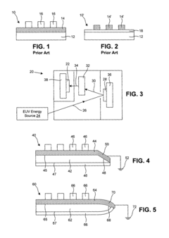
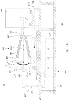
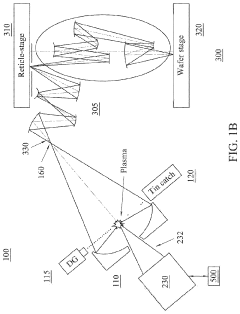
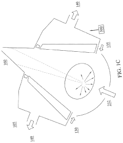
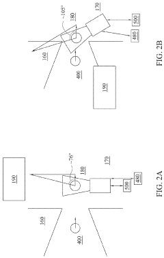
01 EUV Lithography System Design and Components
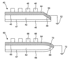
EUV lithography systems incorporate specialized components designed to work with extreme ultraviolet light. These systems typically include radiation sources, optical elements, projection systems, and positioning mechanisms. The design focuses on achieving high resolution and precision while managing the challenges associated with EUV wavelengths, such as vacuum requirements and specialized mirrors.- EUV Lithography System Components: Extreme Ultraviolet (EUV) lithography systems consist of specialized components designed to work with short-wavelength light. These systems include EUV light sources, reflective optics (since EUV is absorbed by traditional lenses), specialized masks, and precise positioning stages. The integration of these components enables the creation of semiconductor devices with feature sizes below 10nm, representing a significant advancement in lithography technology.
- EUV Source Technology: EUV light sources are critical components that generate the extreme ultraviolet radiation needed for lithography. These sources typically use laser-produced plasma or discharge-produced plasma techniques to create EUV radiation at a wavelength of 13.5nm. The development of high-power, stable EUV sources has been a significant challenge in making EUV lithography commercially viable for high-volume manufacturing of advanced semiconductor devices.
- EUV Mask Technology: EUV masks differ significantly from traditional photomasks as they operate in reflection rather than transmission mode. These masks consist of multilayer reflective coatings with absorber patterns on top. The development of defect-free masks and inspection technologies is crucial for EUV lithography. Advanced mask designs incorporate various features to enhance image contrast and resolution, enabling the patterning of increasingly smaller semiconductor features.
- EUV Optics and Alignment Systems: EUV lithography requires highly specialized optical systems consisting of multilayer-coated mirrors that can efficiently reflect EUV radiation. These systems must maintain precise alignment with nanometer-level accuracy during operation. Advanced alignment and positioning systems compensate for thermal effects, vibration, and other disturbances that could affect image quality. The development of stable, high-precision optical systems has been essential for achieving the resolution capabilities of EUV lithography.
- EUV Resist and Process Development: Specialized photoresist materials have been developed to work with EUV radiation. These materials must provide high sensitivity to EUV wavelengths while maintaining the resolution and line edge roughness requirements for advanced semiconductor nodes. The development of EUV-specific processes includes optimization of resist chemistry, post-exposure baking conditions, and development processes. These advancements in materials and processes are critical for realizing the full resolution potential of EUV lithography technology.
02 Contamination Control in EUV Lithography
Contamination control is critical in EUV lithography due to the sensitivity of the process to particles and molecular contaminants. Various methods are employed to prevent and mitigate contamination, including specialized cleaning techniques, protective layers, and environmental controls. These approaches help maintain the integrity of optical surfaces and ensure consistent lithographic performance.Expand Specific Solutions03 Mask Technology for EUV Lithography
EUV masks require specialized technology due to the reflective nature of EUV lithography. These masks typically consist of multilayer reflective coatings with absorber patterns. Innovations in mask design, defect inspection, and repair techniques are essential for achieving high-quality pattern transfer in EUV lithography processes.Expand Specific Solutions04 Metrology and Inspection for EUV Lithography
Specialized metrology and inspection tools are essential for EUV lithography to ensure pattern accuracy and process control. These include systems for measuring overlay, critical dimensions, and defects at nanometer scales. Advanced algorithms and optical configurations enable precise measurements despite the challenges posed by EUV wavelengths and small feature sizes.Expand Specific Solutions05 Source Technology for EUV Lithography
EUV light sources represent a critical component of lithography systems, typically generating light at 13.5nm wavelength. These sources often use laser-produced plasma or discharge-produced plasma technologies to create the high-energy photons needed. Innovations focus on increasing source power, stability, and reliability while managing debris and thermal issues to meet the demanding requirements of high-volume manufacturing.Expand Specific Solutions
Key Industry Players in Medical EUV Applications
EUV lithography in medical device innovations is emerging at an early development stage, with significant growth potential as the technology matures. The market is expanding as semiconductor manufacturing techniques find novel applications in precision medical devices. Among key players, ASML Netherlands BV leads in EUV system development, while Intel, Samsung, and TSMC are adapting this technology for potential medical applications. Research institutions like the Institute of Microelectronics of CAS and Wisconsin Alumni Research Foundation are exploring fundamental applications. Companies with optical expertise such as Nikon, Carl Zeiss SMT, and Cymer are developing specialized components. The competitive landscape shows a blend of established semiconductor giants and specialized research entities collaborating to overcome technical challenges in adapting EUV technology for medical device manufacturing.
Taiwan Semiconductor Manufacturing Co., Ltd.
Technical Solution: TSMC has pioneered the application of EUV lithography for medical device manufacturing through their specialized Medical IC Foundry Service. Their approach integrates EUV patterning with biocompatible materials to create implantable neural interfaces with feature sizes below 5nm. TSMC's medical EUV platform incorporates specialized resist chemistries that meet ISO 10993 biocompatibility standards while maintaining the resolution advantages of EUV lithography. Their process enables the fabrication of ultra-miniaturized biosensors capable of real-time monitoring of multiple biomarkers simultaneously. TSMC has demonstrated the ability to pattern microelectrode arrays with over 10,000 channels per square millimeter using their EUV technology, representing a 10x improvement over previous generation lithography techniques. Their medical device EUV platform includes specialized metrology systems that ensure critical dimensions are maintained across biomedical applications requiring extreme precision.
Strengths: Established manufacturing infrastructure with proven high-volume production capabilities; comprehensive quality management systems compliant with medical device regulations (ISO 13485). Weaknesses: Limited flexibility for customization compared to specialized medical device manufacturers; primarily focused on semiconductor applications with medical devices as a secondary market.
Nikon Corp.
Technical Solution: Nikon has developed specialized EUV lithography tools optimized for medical device manufacturing, leveraging their extensive optical expertise. Their medical EUV platform incorporates proprietary illumination systems that enhance contrast for biocompatible materials while maintaining sub-20nm resolution capabilities. Nikon's approach integrates their EUV technology with specialized metrology systems designed specifically for validating medical device critical dimensions. Their process enables the fabrication of complex microfluidic structures with feature sizes below 10nm, essential for next-generation point-of-care diagnostic devices. Nikon has demonstrated the ability to pattern biocompatible materials with their EUV systems, achieving aspect ratios exceeding 10:1 for high-surface-area biosensor applications. Their medical EUV platform includes specialized alignment systems that maintain overlay accuracy below 2nm across multiple layers, critical for complex implantable medical electronics.
Strengths: Extensive optical expertise and precision engineering capabilities; diversified business with established medical imaging division providing synergistic knowledge. Weaknesses: Smaller market share in EUV lithography compared to ASML; less established ecosystem for EUV process integration.
Critical Patents in Medical-Grade EUV Technology
Extreme ultraviolet (EUV) lithography masks
PatentInactiveUS6984475B1
Innovation
- The EUV lithography mask design incorporates a substrate with a non-planar reflector film and a conductive layer on the backside, allowing for indirect grounding by connecting the reflector film and absorbers to a ground potential without direct mechanical contact, thereby preventing charge buildup and ESD damage.
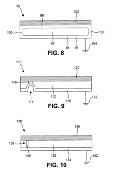
Method and apparatus for mitigating contamination
PatentActiveUS20230273525A1
Innovation
- A supersonic gas jet with high-density hydrogen gas is employed at the intermediate focus to deflect tin nanoparticles away from the reticle, either alone or in combination with a low-level electromagnetic field, ensuring they do not contaminate the scanner side.
Regulatory Framework for EUV-Manufactured Medical Devices
The integration of EUV lithography into medical device manufacturing necessitates a comprehensive regulatory framework to ensure patient safety while enabling innovation. Currently, the FDA in the United States and the European Medicines Agency (EMA) in Europe are developing specialized guidelines for EUV-manufactured medical devices, recognizing their unique characteristics and potential benefits.
These regulatory bodies are focusing on three primary areas: material biocompatibility, structural integrity, and long-term stability of nano-scale features produced through EUV lithography. The unprecedented precision of EUV technology creates regulatory challenges as existing frameworks were not designed with such nanometer-scale capabilities in mind.
The FDA has initiated a Medical Device Innovation Consortium specifically addressing advanced manufacturing technologies, including EUV lithography. This consortium aims to establish testing protocols and validation methodologies appropriate for the unique characteristics of EUV-manufactured devices. Similarly, the International Medical Device Regulators Forum (IMDRF) has formed a working group to harmonize global regulatory approaches to these advanced manufacturing technologies.
Key regulatory considerations include verification and validation protocols for EUV-manufactured components, with particular emphasis on how nanoscale features might interact with biological systems. Regulatory bodies are requiring manufacturers to demonstrate that EUV-specific manufacturing processes do not introduce new biocompatibility concerns or compromise device performance over time.
Quality management systems for EUV manufacturing are also evolving, with ISO 13485 standards being updated to incorporate considerations specific to advanced lithography techniques. These updates focus on process validation, equipment qualification, and specialized training requirements for personnel working with EUV systems in medical device production environments.
Premarket approval pathways are being adapted to accommodate EUV-manufactured devices, with regulatory bodies considering expedited review processes for devices that demonstrate significant advantages over conventionally manufactured alternatives. However, these expedited pathways typically require more robust post-market surveillance commitments.
Post-market surveillance requirements for EUV-manufactured devices are generally more stringent, with regulatory bodies requiring manufacturers to implement comprehensive monitoring systems to detect any unforeseen long-term effects of nanoscale features on device performance or patient outcomes. This includes requirements for specialized testing methodologies capable of evaluating nanoscale structural integrity throughout the device lifecycle.
As the regulatory landscape continues to evolve, manufacturers are advised to engage early and often with regulatory authorities through pre-submission consultations and participation in standards development activities specific to EUV manufacturing technologies in the medical device sector.
Biocompatibility Considerations for EUV-Fabricated Implants
The biocompatibility of medical implants fabricated using EUV lithography represents a critical consideration for clinical applications. EUV lithography enables the creation of nanoscale features on implant surfaces that can significantly influence cell adhesion, tissue integration, and immune response. These nanopatterned surfaces can potentially mimic natural extracellular matrices, promoting favorable biological interactions at the tissue-implant interface.
Material selection for EUV-fabricated implants requires careful evaluation, as the high-energy photons used in the process may alter surface chemistry. Traditional biocompatible materials such as titanium alloys, stainless steel, and certain polymers must be reassessed when subjected to EUV processing. Research indicates that EUV exposure can create unique surface topographies that may enhance osseointegration in orthopedic implants while minimizing bacterial adhesion, addressing the dual challenges of integration and infection.
Residual photoresist materials and process chemicals present particular concerns for biocompatibility. EUV lithography typically employs chemically amplified resists containing photoacid generators and various solvents that must be completely removed before implantation. Advanced cleaning protocols, including oxygen plasma treatment and supercritical CO2 cleaning, have demonstrated effectiveness in removing these potential contaminants without compromising the nanoscale features created through EUV lithography.
Inflammatory responses to EUV-fabricated implants require thorough investigation. Preliminary studies suggest that precisely controlled nanotopography can modulate macrophage polarization toward anti-inflammatory phenotypes, potentially reducing fibrotic encapsulation. However, long-term studies examining chronic inflammation and foreign body responses to these novel surfaces remain limited, highlighting a critical research gap that must be addressed before clinical implementation.
Sterilization compatibility represents another significant challenge. Common sterilization methods such as gamma irradiation, ethylene oxide treatment, and autoclaving may alter the carefully engineered nanoscale features produced by EUV lithography. Research indicates that low-temperature hydrogen peroxide plasma sterilization may preserve these structures while ensuring sterility, though validation across different implant materials and geometries is necessary.
Regulatory considerations for EUV-fabricated implants will require new testing protocols that specifically address the unique characteristics of nanopatterned surfaces. Current biocompatibility testing frameworks (ISO 10993) may need adaptation to properly evaluate these novel implant surfaces, particularly regarding nanoparticle release, surface degradation over time, and long-term tissue interactions in dynamic physiological environments.
Unlock deeper insights with Patsnap Eureka Quick Research — get a full tech report to explore trends and direct your research. Try now!
Generate Your Research Report Instantly with AI Agent
Supercharge your innovation with Patsnap Eureka AI Agent Platform!