

EUV Lithography vs Electron Beam Lithography: A Comprehensive Study
OCT 14, 20259 MIN READ
Generate Your Research Report Instantly with AI Agent
PatSnap Eureka helps you evaluate technical feasibility & market potential.
Lithography Evolution and Objectives
Lithography technology has evolved significantly since its inception in the semiconductor industry, transforming from rudimentary contact printing methods to today's advanced nanoscale patterning techniques. The journey began in the 1960s with proximity printing, progressed through various generations of optical lithography, and has now reached the cutting edge with Extreme Ultraviolet (EUV) and Electron Beam (E-beam) lithography technologies. This evolution has been primarily driven by Moore's Law, which predicted the doubling of transistor density approximately every two years, necessitating continuous miniaturization of semiconductor features.
The historical progression of lithography technologies reveals a consistent trend toward shorter wavelengths to achieve higher resolution. From mercury lamp g-line (436nm) and i-line (365nm) systems in the 1980s, the industry transitioned to excimer laser-based deep ultraviolet (DUV) lithography using KrF (248nm) and ArF (193nm) light sources in the 1990s and 2000s. Each transition enabled smaller feature sizes but also introduced new technical challenges related to optics, photoresist chemistry, and mask technology.
EUV lithography, operating at an extremely short wavelength of 13.5nm, represents the current pinnacle of optical lithography methods. Developed over decades with billions in investment, EUV has finally reached production maturity in recent years. Concurrently, E-beam lithography has evolved as a maskless alternative, using focused electron beams instead of photons to pattern substrates directly, offering exceptional resolution but traditionally limited by throughput constraints.
The primary objective of modern lithography development is to enable continued semiconductor scaling while balancing resolution, throughput, and cost considerations. For EUV lithography, key goals include improving source power for enhanced throughput, reducing stochastic effects that cause line edge roughness, and developing more sensitive photoresists. For E-beam lithography, objectives center on dramatically increasing throughput through multi-beam approaches while maintaining precision and addressing challenges related to proximity effects.
Both technologies aim to support the semiconductor industry's roadmap toward sub-3nm nodes and beyond, enabling next-generation computing architectures, artificial intelligence systems, and quantum computing platforms. Additionally, sustainability has emerged as a critical objective, with efforts focused on reducing the environmental footprint of lithography processes through more efficient energy usage and reduced chemical consumption.
Market Demand Analysis for Advanced Semiconductor Fabrication
The semiconductor industry's demand for advanced lithography technologies has been growing exponentially, driven by the continuous pursuit of Moore's Law and the need for smaller, more powerful, and energy-efficient electronic devices. As node sizes shrink below 10nm, traditional optical lithography methods face fundamental physical limitations, creating substantial market demand for next-generation lithography solutions like EUV (Extreme Ultraviolet) and Electron Beam Lithography.
The global semiconductor fabrication equipment market, valued at approximately $80 billion in 2022, is projected to reach $120 billion by 2027, with lithography equipment representing about 30% of this market. EUV lithography systems, primarily supplied by ASML, command prices exceeding $150 million per unit, reflecting both their technological sophistication and the critical market need they address.
Leading semiconductor manufacturers including TSMC, Samsung, and Intel have collectively invested over $50 billion in EUV technology implementation, demonstrating strong market confidence in this approach for high-volume manufacturing at advanced nodes. The demand is particularly acute in the production of logic chips for AI processors, high-performance computing, and mobile SoCs, where feature density and performance gains translate directly to competitive advantage.
Electron Beam Lithography, while representing a smaller market segment valued at approximately $1.5 billion, serves crucial niche applications in mask making, research and development, and low-volume specialty semiconductor production. The market for multi-beam e-beam systems is growing at 15% annually, driven by increasing mask complexity for advanced nodes and emerging applications in direct-write manufacturing for specialized chips.
Regional analysis reveals Asia-Pacific dominates the advanced lithography market with over 65% share, led by Taiwan and South Korea's massive fab investments. North America and Europe follow with significant investments in both technologies, particularly as concerns about semiconductor supply chain resilience drive reshoring initiatives.
Customer segmentation shows that while major IDMs and foundries primarily drive EUV adoption, research institutions, specialized foundries, and mask shops constitute the core market for e-beam lithography. This differentiation reflects the complementary nature of these technologies in the semiconductor ecosystem.
Market forecasts indicate EUV lithography will continue its rapid growth trajectory, with an installed base expected to triple by 2028. Meanwhile, e-beam lithography will see more modest but steady growth, with increasing adoption of multi-beam systems for specialized manufacturing applications where EUV's economics are less favorable.
EUV and E-Beam Lithography: Current Status and Challenges
The current landscape of advanced lithography is dominated by two key technologies: Extreme Ultraviolet (EUV) Lithography and Electron Beam (E-Beam) Lithography, each with distinct technological profiles and implementation challenges. EUV lithography, operating at a 13.5nm wavelength, has achieved significant commercial deployment in high-volume manufacturing environments, primarily led by ASML as the sole equipment provider. The technology enables feature sizes below 7nm, supporting the semiconductor industry's continued adherence to Moore's Law.
Despite its commercial success, EUV lithography faces substantial technical challenges. The generation and management of EUV light remains inefficient, with current systems achieving only 2-3% conversion efficiency from laser energy to usable EUV radiation. This inefficiency necessitates extremely high-powered lasers, creating thermal management issues and increasing operational costs. Additionally, EUV requires specialized vacuum environments and highly reflective mirrors with complex multilayer designs, as traditional refractive optics absorb EUV radiation.
E-Beam lithography, conversely, offers superior resolution capabilities by directly writing patterns using focused electron beams without requiring masks. This technology can achieve sub-5nm features with exceptional precision. However, its throughput limitations have historically restricted its use to research environments and mask production rather than high-volume manufacturing. Recent innovations in multi-beam systems have partially addressed this limitation, with tools featuring thousands of parallel beams showing promise for commercial applications.
Geographically, EUV technology development is concentrated in specific regions, with the Netherlands (ASML), Germany (Zeiss for optics), and Japan (laser and component suppliers) forming the primary innovation hubs. E-Beam technology development is more distributed, with significant contributions from Japan (JEOL), Germany (Vistec), and the United States (Applied Materials).
Both technologies face materials challenges, particularly in developing resists that balance sensitivity, resolution, and line-edge roughness. EUV-specific challenges include stochastic effects at extreme dimensions and mask defectivity issues, while E-Beam confronts proximity effect correction complexities and charging problems during exposure.
The economic barriers to entry differ significantly between these technologies. EUV systems represent extraordinary capital investments (>$150 million per tool), limiting their adoption to major semiconductor manufacturers. E-Beam systems, while less expensive individually, face economic viability challenges in production environments due to their throughput limitations, though they remain essential for specialized applications and advanced research.
Comparative Analysis of EUV and E-Beam Solutions
01 EUV Lithography Systems and Components
Extreme Ultraviolet (EUV) lithography systems utilize short wavelength light to achieve high-resolution patterning for semiconductor manufacturing. These systems include specialized components such as radiation sources, mirrors, and optical elements designed to work with EUV wavelengths. The technology enables the production of smaller feature sizes on semiconductor wafers, advancing the capabilities of integrated circuit manufacturing beyond traditional optical lithography limitations.- EUV Lithography Systems and Components: Extreme Ultraviolet (EUV) lithography systems utilize short wavelength light for high-resolution semiconductor manufacturing. These systems include specialized components such as reflective optics, radiation sources, and mask technologies designed to work with EUV wavelengths. The systems enable the production of smaller feature sizes on semiconductor wafers, advancing chip manufacturing capabilities beyond traditional optical lithography limits.
- Electron Beam Lithography Technology: Electron Beam Lithography (EBL) uses focused beams of electrons to create patterns on substrates. This technology offers higher resolution than optical methods by directly writing patterns without masks. EBL systems incorporate electron sources, beam focusing mechanisms, and precise stage control systems to achieve nanometer-scale features. This technology is particularly valuable for research, prototype development, and mask fabrication.
- Hybrid and Complementary Lithography Approaches: Combining EUV and electron beam lithography with other techniques creates hybrid approaches that leverage the strengths of each method. These complementary strategies may involve using electron beam for critical layers and EUV for others, or employing multiple patterning techniques. Such hybrid approaches help overcome resolution limitations, reduce costs, or address specific manufacturing challenges in advanced semiconductor fabrication.
- Radiation Sources and Beam Generation: Advanced radiation sources are critical components for both EUV and electron beam lithography systems. For EUV, plasma-based sources generate the required short-wavelength radiation, while electron beam systems utilize electron guns with precise emission control. These sources require sophisticated mechanisms for beam generation, focusing, and energy management to achieve the stability and intensity needed for high-resolution lithography.
- Resist Materials and Process Optimization: Specialized resist materials are developed specifically for EUV and electron beam lithography to enhance sensitivity, resolution, and pattern fidelity. These materials are engineered to respond optimally to the specific radiation type while minimizing issues like proximity effects and pattern collapse. Process optimization techniques include exposure dose control, development parameters, and post-exposure treatments that maximize the performance of these advanced lithography methods.
02 Electron Beam Lithography Equipment
Electron Beam Lithography (EBL) equipment uses focused beams of electrons to create patterns on substrates. These systems include electron sources, beam forming optics, and precise positioning stages to achieve nanometer-scale resolution. EBL offers advantages in creating extremely fine features without the need for masks, making it particularly valuable for research, prototyping, and specialized manufacturing applications where high precision is required.Expand Specific Solutions03 Resist Materials and Processing
Specialized resist materials are essential for both EUV and electron beam lithography processes. These materials are designed to undergo chemical changes when exposed to radiation, enabling pattern transfer to the substrate. The development of high-sensitivity, high-resolution resists with appropriate etch resistance properties is crucial for advancing lithography capabilities. Processing techniques, including pre-baking, exposure, post-exposure baking, and development, significantly impact the final pattern quality.Expand Specific Solutions04 Hybrid and Multi-beam Approaches
Hybrid lithography approaches combine multiple patterning technologies to overcome limitations of individual methods. Multi-beam systems use multiple electron beams operating in parallel to increase throughput while maintaining high resolution. These approaches address challenges in semiconductor manufacturing by balancing resolution, throughput, and cost considerations. Integration of complementary techniques enables more efficient production of complex semiconductor devices.Expand Specific Solutions05 Contamination Control and System Optimization
Contamination control is critical in advanced lithography systems to maintain performance and reliability. Methods include specialized vacuum systems, particle detection, and mitigation strategies to prevent contamination of optical elements and substrates. System optimization involves precise calibration, alignment, and correction techniques to maximize resolution and throughput while minimizing defects. These measures are essential for achieving consistent results in high-volume manufacturing environments.Expand Specific Solutions
Key Industry Players in Lithography Equipment Manufacturing
The EUV Lithography vs Electron Beam Lithography market is in a transitional growth phase, with the global semiconductor lithography equipment market valued at approximately $15 billion and growing steadily. EUV technology, dominated by ASML Holding NV, has achieved commercial maturity for high-volume manufacturing at advanced nodes, while Electron Beam Lithography remains primarily in R&D and specialized applications. Key players include TSMC and Samsung as leading adopters of EUV technology, with Intel and IBM pursuing strategic implementations. Equipment manufacturers like Applied Materials, Nikon, and D2S continue developing complementary technologies, while research institutions such as MIT and Fudan University drive innovation in next-generation lithography solutions to address semiconductor scaling challenges.
Taiwan Semiconductor Manufacturing Co., Ltd.
Technical Solution: TSMC has pioneered the implementation of EUV lithography in high-volume manufacturing, beginning with their 7nm+ process and expanding to their 5nm and 3nm nodes. Their approach integrates EUV with complementary technologies like self-aligned quadruple patterning (SAQP) to optimize cost and performance. TSMC's EUV implementation includes custom-developed computational lithography techniques that compensate for mask 3D effects and optimize source-mask combinations. They've developed specialized resist materials with their chemical suppliers that balance sensitivity, resolution, and line-edge roughness requirements specific to their process flows. TSMC has also created innovative solutions for EUV-specific defect inspection and metrology, including machine learning algorithms that predict and mitigate stochastic defects. Their fabs incorporate specialized infrastructure modifications to support EUV tools, including enhanced vibration isolation, temperature control systems accurate to ±0.01°C, and custom reticle handling systems that minimize contamination risks.
Strengths: Unmatched production experience with EUV in high-volume manufacturing; sophisticated integration of EUV with complementary patterning techniques; advanced defect detection and mitigation strategies. Weaknesses: Heavy dependence on ASML as the sole EUV equipment supplier; significant capital expenditure requirements for EUV implementation; ongoing challenges with EUV-specific yield management at leading nodes.
ASML Netherlands BV
Technical Solution: ASML is the dominant player in EUV lithography technology, having developed the industry-standard TWINSCAN NXE platform. Their EUV systems operate at 13.5nm wavelength using laser-produced plasma sources that generate extreme ultraviolet light when tin droplets are hit with high-powered CO2 lasers. The latest EUV systems (NXE:3600D) deliver resolution capabilities down to 13nm with throughput of over 160 wafers per hour. ASML's technology incorporates sophisticated computational lithography, including optical proximity correction and source mask optimization, to enhance pattern fidelity. Their systems utilize a complex series of multilayer mirrors with more than 100 alternating layers of molybdenum and silicon, each only a few nanometers thick, to reflect and focus the EUV light with minimal loss. The vacuum environment and specialized reticle infrastructure represent significant engineering achievements that have made high-volume manufacturing with EUV commercially viable.
Strengths: Industry-leading throughput (>160 wafers/hour) enabling economic viability for high-volume manufacturing; superior resolution capabilities enabling advanced node production at 5nm and below; established ecosystem with major semiconductor manufacturers. Weaknesses: Extremely high system cost ($150+ million per tool); significant power consumption requirements; ongoing challenges with stochastic effects at smaller nodes.
Critical Patents and Technical Innovations in Lithography
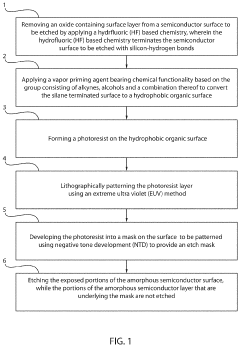
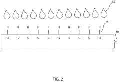
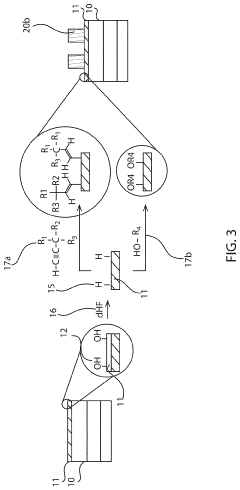
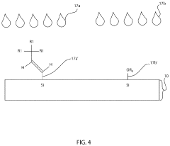
Method to improve adhesion of photoresist on silicon substrate for extreme ultraviolet and electron beam lithography
PatentInactiveUS20200090936A1
Innovation
- The method involves stripping the native oxide layer from the silicon surface using diluted hydrofluoric acid to create a silane-terminated surface, followed by applying a vapor priming agent with alkynes or alcohols to form a hydrophobic organic surface, enhancing the adhesion of EUV resists during TMAH development.
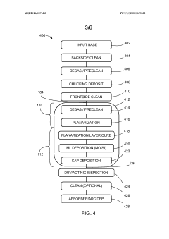
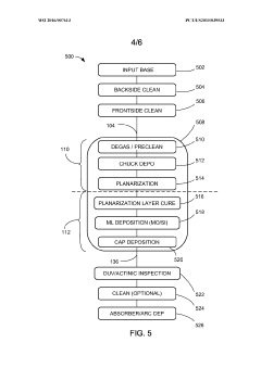
Planarized extreme ultraviolet lithography blank with absorber and manufacturing system therefor
PatentWO2016007613A1
Innovation
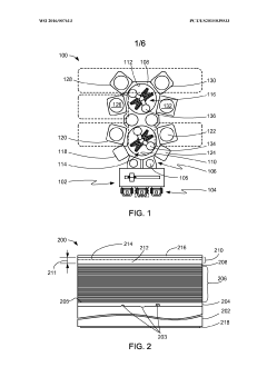
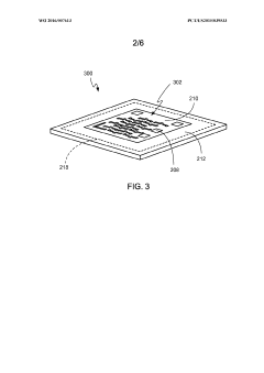
- A planarized extreme ultraviolet lithography blank system with a bi-layer absorber and manufacturing process that includes a substrate handling vacuum chamber, ultra-low expansion substrate, planarization layer, multi-layer stack, and a bi-layer absorber with a primary and secondary absorber layer combination to minimize reflectivity and surface defects, using materials like silver and nickel to achieve low reflectivity and reduce shadowing.
Economic Implications of Lithography Technology Selection
The economic implications of lithography technology selection extend far beyond the initial capital investment, encompassing operational costs, production efficiency, and market competitiveness. EUV lithography systems represent a significant capital expenditure, with each tool costing approximately $120-150 million, compared to electron beam lithography systems at $10-30 million. However, this substantial price differential must be contextualized within broader economic considerations.
For high-volume manufacturing scenarios, EUV lithography demonstrates superior economic efficiency despite its higher initial cost. The throughput advantage of EUV systems—processing 100-125 wafers per hour versus 0.1-1 wafers per hour for electron beam systems—translates to dramatically lower cost per wafer in mass production environments. This throughput differential becomes the decisive economic factor for semiconductor manufacturers serving consumer electronics and other high-volume markets.
Conversely, electron beam lithography presents compelling economic advantages in low-volume, high-precision applications such as photomask production, prototype development, and specialized research environments. The lower capital investment and reduced infrastructure requirements make e-beam technology financially viable for smaller organizations, research institutions, and specialized manufacturing operations where throughput is less critical than precision or flexibility.
Maintenance and operational costs further differentiate these technologies economically. EUV systems require specialized infrastructure including vacuum systems, hydrogen supply, and sophisticated optical components that demand regular maintenance and replacement. The consumables for EUV, particularly the tin droplets used for plasma generation and complex mirror systems, represent ongoing operational expenses that must be factored into total cost of ownership calculations.
The economic landscape is also shaped by supply chain considerations. The limited number of EUV equipment suppliers—with ASML holding a near-monopoly position—creates potential pricing pressures and supply constraints that impact adoption economics. In contrast, the electron beam lithography market features multiple suppliers, fostering more competitive pricing dynamics.
From a strategic economic perspective, technology selection influences a manufacturer's market positioning and competitive advantage. EUV adoption enables production of cutting-edge semiconductor devices with higher performance and energy efficiency, potentially commanding premium pricing. This technology-enabled market differentiation must be weighed against the substantial capital investment when making lithography technology decisions.
Environmental and Resource Considerations in Advanced Lithography
Both EUV (Extreme Ultraviolet) and Electron Beam Lithography represent cutting-edge semiconductor manufacturing technologies, yet their environmental footprints and resource requirements differ significantly. The environmental impact of these advanced lithography techniques has become increasingly important as the semiconductor industry faces growing scrutiny regarding sustainability practices.
EUV lithography systems consume substantial amounts of energy, with a single tool requiring up to 1 MW of power during operation. This high energy demand stems from the complex process of generating EUV light, which involves creating plasma from tin droplets using high-powered CO2 lasers. The cooling systems necessary to maintain optimal operating conditions further contribute to the energy footprint. Additionally, EUV requires specialized gases and chemicals, including hydrogen and fluorine compounds, which present both handling risks and disposal challenges.
In contrast, Electron Beam Lithography demonstrates lower overall energy consumption but faces efficiency limitations. While individual e-beam systems use less power than EUV tools, their slower throughput often necessitates multiple machines running simultaneously to match production volumes, potentially offsetting the per-unit energy advantage. E-beam systems also require fewer specialized gases but still utilize various chemicals for resist development and processing.
Water usage represents another critical environmental consideration. EUV systems require substantial volumes of ultra-pure water for cooling and cleaning processes, with estimates suggesting consumption of thousands of liters per hour during peak operation. E-beam systems generally have lower water requirements but still contribute significantly to the semiconductor industry's water footprint.
Raw material sourcing presents sustainability challenges for both technologies. EUV systems rely on rare earth elements and specialized materials for mirrors and optical components, while e-beam systems require high-purity materials for electron sources and electromagnetic components. The extraction and processing of these materials often involve environmentally intensive mining operations and complex supply chains with varying levels of environmental governance.
Waste management differs between the technologies as well. EUV generates specific waste streams including tin residues and specialized optical cleaning compounds. E-beam lithography produces fewer specialized waste products but still generates standard semiconductor manufacturing waste including spent resists and development chemicals. Both technologies contribute to the semiconductor industry's challenge of managing hazardous waste streams that require specialized treatment and disposal protocols.
Unlock deeper insights with PatSnap Eureka Quick Research — get a full tech report to explore trends and direct your research. Try now!
Generate Your Research Report Instantly with AI Agent
Supercharge your innovation with PatSnap Eureka AI Agent Platform!