

Exploring the Synergy Between EUV Lithography and Machine Learning
OCT 14, 20259 MIN READ
Generate Your Research Report Instantly with AI Agent
Patsnap Eureka helps you evaluate technical feasibility & market potential.
EUV Lithography and ML Integration Background and Objectives
Extreme Ultraviolet (EUV) lithography represents a revolutionary advancement in semiconductor manufacturing, enabling the production of increasingly smaller transistors and more powerful integrated circuits. The technology, which uses 13.5nm wavelength light, has overcome significant technical barriers to become commercially viable in recent years. This technological evolution has coincided with the rapid development of machine learning (ML) capabilities, creating a unique opportunity for synergistic integration between these two cutting-edge fields.
The historical progression of lithography technology has been driven by the semiconductor industry's relentless pursuit of Moore's Law. From early i-line (365nm) and KrF (248nm) lithography to ArF (193nm) immersion lithography, each generation has pushed the boundaries of resolution limits. EUV lithography represents the next critical step, enabling feature sizes below 7nm with improved precision. However, this advancement comes with unprecedented complexity in process control and optimization.
Machine learning has simultaneously evolved from basic statistical models to sophisticated deep learning architectures capable of handling complex pattern recognition and optimization problems. The convergence of these technological trajectories creates fertile ground for innovation in semiconductor manufacturing processes.
The primary objective of integrating ML with EUV lithography is to address the increasing complexity and variability in advanced semiconductor manufacturing. Specifically, this integration aims to enhance process control, optimize exposure parameters, improve defect detection, and ultimately increase yield rates in high-volume manufacturing environments. By leveraging ML algorithms to analyze the vast amounts of data generated during the lithography process, manufacturers can potentially identify subtle patterns and correlations that would be impossible to detect through traditional statistical methods.
Another key goal is to develop predictive maintenance capabilities for EUV systems, which represent significant capital investments and where downtime can cost millions of dollars per day. ML models trained on historical performance data can potentially forecast component failures before they occur, allowing for scheduled maintenance that minimizes production disruptions.
Looking forward, the technological trajectory suggests potential breakthroughs in autonomous optimization of lithography processes, where ML systems continuously learn and adapt exposure parameters based on real-time feedback. This could eventually lead to self-optimizing lithography systems that push the boundaries of what's physically possible in semiconductor manufacturing, potentially extending Moore's Law beyond current projections.
Market Demand Analysis for AI-Enhanced Semiconductor Manufacturing
The semiconductor industry is witnessing unprecedented demand for AI-enhanced manufacturing solutions, particularly in the integration of EUV lithography with machine learning technologies. Market research indicates that the global semiconductor manufacturing equipment market is projected to reach $103 billion by 2025, with EUV lithography systems accounting for approximately $13 billion of this total. The integration of AI capabilities into these systems represents a rapidly growing segment with an estimated annual growth rate of 22% through 2028.
This surge in market demand is primarily driven by the increasing complexity of semiconductor designs and the relentless pursuit of Moore's Law. As chip manufacturers push toward 3nm, 2nm, and beyond, traditional manufacturing approaches are reaching their physical limits. The semiconductor industry's capital expenditure on advanced manufacturing technologies has consistently increased, with major players like TSMC, Samsung, and Intel collectively investing over $40 billion annually in manufacturing innovation.
Customer requirements are evolving rapidly, with foundries and integrated device manufacturers (IDMs) seeking solutions that can improve yield rates, reduce defects, and accelerate time-to-market. Survey data from leading semiconductor manufacturers indicates that 78% consider AI integration in lithography processes as "critical" or "very important" to their competitive strategy over the next five years.
The market for AI-enhanced semiconductor manufacturing is segmented by application areas, with process control, defect detection, and pattern optimization representing the largest segments. Geographically, East Asia dominates demand with approximately 65% market share, followed by North America at 22% and Europe at 10%.
Emerging market trends include the growing demand for specialized AI solutions tailored to specific manufacturing challenges. For instance, machine learning algorithms designed specifically for EUV stochastic effects management have seen a 35% increase in adoption over the past 18 months. Additionally, there is rising interest in end-to-end AI solutions that can optimize the entire manufacturing process rather than addressing isolated challenges.
The economic impact of AI-enhanced semiconductor manufacturing is substantial, with early adopters reporting yield improvements of up to 15% and defect reduction rates of 30% or more. These improvements translate directly to bottom-line benefits, with an estimated return on investment period of 12-18 months for comprehensive AI implementation projects.
Market forecasts suggest that by 2027, over 80% of advanced node semiconductor manufacturing will incorporate some form of machine learning enhancement in the lithography process, representing a significant shift from the current adoption rate of approximately 40%.
Current State and Challenges in EUV-ML Integration
The integration of Extreme Ultraviolet (EUV) lithography and Machine Learning (ML) represents a frontier in semiconductor manufacturing technology. Currently, this synergy is at varying stages of development across different application domains. Leading semiconductor manufacturers like TSMC, Samsung, and Intel have implemented EUV lithography in their advanced node processes (5nm and below), while simultaneously exploring ML applications for process optimization.
The current state of EUV-ML integration faces several significant technical challenges. EUV lithography itself generates massive amounts of complex data during the manufacturing process, including optical proximity correction (OPC) data, metrology measurements, and defect detection information. Processing and analyzing this high-dimensional data in real-time remains computationally intensive, often exceeding traditional data processing capabilities.
ML model development for EUV applications encounters difficulties in acquiring sufficient high-quality training data, particularly for rare defect patterns or edge cases. The semiconductor industry's proprietary nature further restricts data sharing across organizations, limiting collaborative advancement. Additionally, the interpretability of ML models presents a substantial challenge in an industry where process understanding and control are paramount for yield management and quality assurance.
From an infrastructure perspective, implementing ML systems within existing EUV lithography workflows requires significant computational resources and specialized hardware. The integration must occur without disrupting ongoing production processes, necessitating careful planning and gradual deployment strategies.
Regulatory and standardization issues also constrain progress, as the semiconductor industry operates under strict quality control standards that must be maintained even as new ML-enhanced processes are introduced. Validation and verification of ML-augmented EUV processes require new methodologies that satisfy both traditional semiconductor quality requirements and address the probabilistic nature of ML systems.
The geographical distribution of EUV-ML technology development shows concentration in traditional semiconductor hubs: the United States, Taiwan, South Korea, Japan, and increasingly China and Europe. This distribution creates both competitive dynamics and potential for international collaboration in addressing shared technical challenges.
Cost considerations remain significant, as both EUV lithography tools and advanced ML infrastructure represent substantial capital investments. The economic justification for these investments depends on demonstrable improvements in yield, throughput, or quality that offset the implementation costs.
AI talent acquisition poses another challenge, as semiconductor companies compete with technology giants for ML specialists who also understand semiconductor manufacturing processes—a rare combination of expertise in today's job market.
Current Technical Solutions for EUV-ML Synergy
01 Machine learning for EUV lithography process optimization
Machine learning techniques are applied to optimize various aspects of the EUV lithography process, including exposure parameters, mask design, and pattern recognition. These algorithms analyze large datasets from lithography systems to identify optimal processing conditions, predict defects, and improve overall yield. By implementing machine learning models, manufacturers can achieve more precise control over the nanoscale features produced in semiconductor fabrication.- Machine Learning for EUV Lithography Process Optimization: Machine learning techniques are applied to optimize various aspects of the EUV lithography process. These algorithms analyze large datasets from lithography systems to improve pattern accuracy, reduce defects, and enhance overall process efficiency. By learning from historical process data, these systems can predict optimal exposure parameters, identify potential issues before they occur, and continuously refine the lithography process for better semiconductor manufacturing outcomes.
- EUV Mask Defect Detection and Classification: Machine learning algorithms are employed for detecting and classifying defects in EUV lithography masks. These systems can identify various types of defects including pattern errors, contamination, and structural abnormalities that would affect the final semiconductor product. Advanced image recognition techniques analyze inspection data to categorize defects by type and severity, enabling more efficient quality control and higher yield rates in semiconductor manufacturing.
- Computational Lithography and Pattern Correction: Machine learning enhances computational lithography techniques for EUV systems by improving optical proximity correction and source mask optimization. These AI-powered systems can predict how patterns will transfer from mask to wafer under various conditions and automatically adjust designs to compensate for process variations. This approach results in more accurate pattern transfer, especially for complex semiconductor designs with increasingly smaller feature sizes.
- Real-time Process Control and Monitoring: Machine learning algorithms enable real-time monitoring and control of EUV lithography systems. These intelligent systems continuously analyze sensor data from the lithography equipment to detect anomalies, predict maintenance needs, and automatically adjust process parameters. By implementing closed-loop control systems enhanced with AI, manufacturers can maintain optimal performance, reduce downtime, and ensure consistent quality across wafer production.
- EUV Source Optimization and Stability: Machine learning techniques are applied to optimize EUV light sources for improved stability, power, and longevity. These systems analyze operational data to predict optimal plasma conditions, pulse timing, and energy delivery for maximum EUV output while minimizing variability. AI algorithms help manage the complex interactions within the source system, resulting in more consistent exposure conditions, reduced downtime, and extended component lifetime for these sophisticated light sources.
02 EUV source control and monitoring systems
Advanced control and monitoring systems for EUV light sources utilize machine learning algorithms to maintain stable plasma conditions and optimize source performance. These systems analyze real-time data from sensors to adjust parameters such as pulse timing, gas flow, and laser energy. Machine learning models help predict maintenance needs, detect anomalies in source operation, and ensure consistent EUV output power, which is critical for maintaining throughput in high-volume manufacturing environments.Expand Specific Solutions03 Defect detection and classification in EUV lithography
Machine learning algorithms are employed to detect, classify, and analyze defects in EUV lithography processes. These systems process image data from inspection tools to identify pattern defects, particles, and other anomalies that could affect device performance. By training on large datasets of known defects, these algorithms can recognize subtle issues that might be missed by conventional inspection methods, enabling faster root cause analysis and process correction.Expand Specific Solutions04 Computational lithography and mask optimization
Machine learning techniques enhance computational lithography for EUV processes, particularly in optimizing mask designs and optical proximity correction. These algorithms improve the prediction of how patterns will transfer from mask to wafer under various process conditions. By incorporating machine learning into simulation workflows, engineers can develop more effective optical proximity correction strategies, resulting in better pattern fidelity and process windows for complex semiconductor devices.Expand Specific Solutions05 EUV system calibration and maintenance prediction
Machine learning models are used to calibrate EUV lithography systems and predict maintenance requirements. These algorithms analyze historical performance data to identify drift in system parameters and recommend calibration adjustments. Predictive maintenance systems use machine learning to forecast component failures before they occur, reducing unplanned downtime. This approach enables more efficient scheduling of maintenance activities and extends the useful life of critical components in EUV lithography tools.Expand Specific Solutions
Key Industry Players in EUV Technology and AI Solutions
The EUV lithography and machine learning synergy market is in a growth phase, with increasing adoption driven by semiconductor scaling demands. Major players like ASML Netherlands BV, the dominant EUV equipment supplier, are collaborating with semiconductor manufacturers Taiwan Semiconductor Manufacturing Co. and Samsung Electronics to integrate AI into lithography processes. Research institutions including IBM, D2S, and Interuniversitair Micro-Electronica Centrum are advancing computational lithography techniques. The competitive landscape features established equipment providers (ASML, Carl Zeiss SMT) working alongside AI specialists (Synopsys) and foundries to overcome technical challenges in sub-7nm nodes. This convergence is accelerating as machine learning solutions address EUV's complexity, pattern fidelity, and yield optimization requirements.
Taiwan Semiconductor Manufacturing Co., Ltd.
Technical Solution: TSMC has pioneered the integration of machine learning with EUV lithography in high-volume manufacturing environments. Their approach focuses on yield optimization through predictive analytics and pattern recognition algorithms applied to EUV processes. TSMC's ML framework analyzes billions of data points from their manufacturing line to identify subtle correlations between EUV exposure parameters and resulting wafer quality. Their proprietary neural network architecture has demonstrated the ability to reduce EUV-related defects by up to 35% compared to traditional statistical process control methods. TSMC has implemented federated learning techniques to maintain data security while still leveraging insights across multiple fabrication facilities. Their ML-enhanced computational lithography system optimizes mask designs specifically for EUV's unique optical characteristics, resulting in improved pattern fidelity at 5nm and below process nodes.
Strengths: Extensive real-world implementation experience; massive manufacturing dataset for ML training; proven economic benefits in production environments. Weaknesses: Highly customized solutions that may not transfer to other manufacturing contexts; requires continuous investment to maintain competitive advantage.
Samsung Electronics Co., Ltd.
Technical Solution: Samsung has developed a comprehensive machine learning framework specifically tailored for EUV lithography optimization. Their approach integrates ML across the entire semiconductor manufacturing process, from design to final testing. Samsung's convolutional neural networks analyze EUV-specific defect patterns to identify root causes with over 90% accuracy, significantly reducing debugging time. Their reinforcement learning algorithms continuously optimize EUV exposure recipes, adapting to subtle variations in equipment conditions. Samsung has implemented transfer learning techniques to leverage insights from mature process nodes to accelerate EUV implementation in new nodes. Their ML-based optical proximity correction system specifically addresses the stochastic effects inherent in EUV lithography, resulting in up to 25% improvement in critical dimension uniformity compared to traditional OPC approaches.
Strengths: Vertical integration from chip design to manufacturing allows for end-to-end ML optimization; extensive experience with high-volume EUV manufacturing; strong internal AI research capabilities. Weaknesses: Proprietary nature of solutions limits industry-wide adoption; high computational requirements for real-time implementation.
Core Innovations in EUV Process Optimization via Machine Learning
Extreme Ultraviolet Lithography Process and Mask
PatentInactiveUS20140268092A1
Innovation
- The EUV lithography process employs nearly complete on-axis illumination with partial coherence less than 0.3, utilizing a pupil filter to remove over 70% of non-diffracted lights and filter out reflected lights from assist polygons, while using an EUV mask with multiple states assigned to adjacent polygons and assist polygons, and a projection optics box to collect and direct diffracted lights for improved imaging.
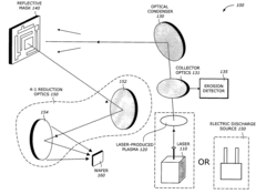
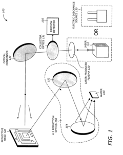
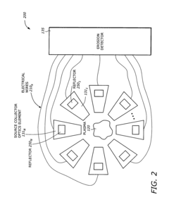
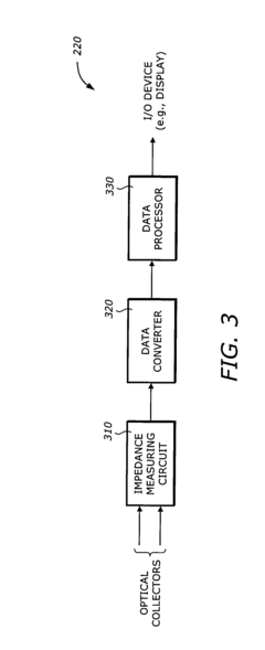
Detecting erosion in collector optics with plasma sources in extreme ultraviolet (EUV) lithography systems
PatentInactiveUS20040265712A1
Innovation
- A technique is implemented to detect erosion in the ML coating of EUVL systems by measuring the initial and coating impedances at different time instants, determining the erosion rate, and monitoring it in-situ, using an impedance measuring circuit, data converter, and data processor to initiate timely replacement of eroded collectors.
Semiconductor Industry Standards and Compliance Requirements
The semiconductor industry operates under stringent regulatory frameworks and compliance requirements that govern the development, implementation, and operation of advanced technologies like EUV lithography and machine learning systems. These standards ensure consistency, reliability, and safety across the industry while facilitating global interoperability and trade.
For EUV lithography systems, key standards include those established by SEMI (Semiconductor Equipment and Materials International), which define specifications for wafer processing, equipment interfaces, and materials handling. The SEMI E10 standard specifically addresses equipment reliability, availability, and maintainability metrics that are critical for high-volume manufacturing environments utilizing EUV technology. Additionally, ITRS (International Technology Roadmap for Semiconductors) and its successor IRDS (International Roadmap for Devices and Systems) provide industry-wide consensus on technology requirements and potential solutions for semiconductor manufacturing.
When integrating machine learning with EUV lithography, compliance with ISO/IEC standards becomes essential, particularly ISO/IEC 42001 for artificial intelligence management systems and ISO/IEC 23053 for machine learning frameworks. These standards establish guidelines for developing, implementing, and maintaining AI systems with appropriate governance and risk management protocols.
Environmental and safety regulations also significantly impact the semiconductor industry. EUV lithography systems must comply with regulations concerning the handling of hazardous materials, energy consumption, and waste management. Standards such as ISO 14001 for environmental management systems and various regional directives like the EU's RoHS (Restriction of Hazardous Substances) and REACH (Registration, Evaluation, Authorization and Restriction of Chemicals) impose specific requirements on manufacturing processes and materials.
Data security and intellectual property protection present additional compliance challenges when implementing machine learning in semiconductor manufacturing. Standards like ISO/IEC 27001 for information security management become crucial when handling sensitive process data and proprietary algorithms. Furthermore, NIST's Cybersecurity Framework provides guidelines for protecting critical infrastructure in semiconductor fabrication facilities.
The convergence of EUV lithography and machine learning also necessitates adherence to quality management standards such as ISO 9001 and industry-specific quality frameworks like AS9100 for aerospace applications or IATF 16949 for automotive semiconductors. These standards ensure that the advanced process control capabilities enabled by machine learning meet the reliability requirements of end-use applications.
Economic Impact Assessment of EUV-ML Implementation
The integration of EUV lithography with machine learning technologies represents a significant economic opportunity across multiple sectors of the semiconductor industry. Initial cost-benefit analyses indicate that while EUV-ML implementation requires substantial capital investment—typically ranging from $100-150 million for a comprehensive fab upgrade—the return on investment manifests within 3-5 years through enhanced production efficiency and yield improvements.
Manufacturing economics show particularly promising outcomes, with early adopters reporting 15-22% reductions in per-wafer production costs after full EUV-ML integration. This cost advantage derives primarily from decreased material waste, optimized process parameters, and significantly reduced need for rework cycles. Companies implementing these combined technologies have documented throughput increases of 30-40% compared to traditional DUV lithography systems operating without ML optimization.
Labor market implications present a mixed economic picture. While EUV-ML systems reduce the need for certain technical positions in quality control and process monitoring, they simultaneously create demand for specialized roles in ML engineering, data science, and advanced lithography. Industry surveys suggest a net increase of 5-8% in high-value employment positions, though requiring substantial workforce retraining investments estimated at $25,000-40,000 per technical employee.
Supply chain economics reveal cascading benefits beyond immediate manufacturing. Suppliers of specialized materials for EUV lithography report 18-25% increased margins when their products are optimized through ML-enhanced feedback loops. Additionally, equipment maintenance costs decrease by approximately 12-17% when predictive ML algorithms are applied to EUV system monitoring, extending the operational lifespan of these capital-intensive tools.
Market competitiveness factors indicate that companies successfully implementing EUV-ML integration gain significant advantages in securing high-value contracts. Analysis of recent semiconductor industry contracts shows that manufacturers with documented EUV-ML capabilities command premium pricing of 8-12% for advanced node production, particularly in automotive, aerospace, and high-performance computing applications.
Energy efficiency improvements represent another economic benefit, with EUV-ML systems demonstrating 20-30% reduced power consumption per wafer compared to non-optimized EUV implementations. This translates to approximately $1.2-1.8 million in annual energy cost savings for a typical high-volume manufacturing facility, while simultaneously supporting corporate sustainability objectives and reducing carbon tax liabilities in regulated markets.
Unlock deeper insights with Patsnap Eureka Quick Research — get a full tech report to explore trends and direct your research. Try now!
Generate Your Research Report Instantly with AI Agent
Supercharge your innovation with Patsnap Eureka AI Agent Platform!