

What Are the Primary Technical Challenges in EUV Lithography
OCT 14, 20259 MIN READ
Generate Your Research Report Instantly with AI Agent
PatSnap Eureka helps you evaluate technical feasibility & market potential.
EUV Lithography Evolution and Objectives
Extreme Ultraviolet (EUV) lithography represents a revolutionary advancement in semiconductor manufacturing, emerging after decades of research and development efforts. The technology's evolution began in the 1980s with initial conceptual work, but significant progress only materialized in the early 2000s when industry consortiums like ASML, Carl Zeiss, and Cymer intensified collaborative research efforts. This technological journey has been driven by the semiconductor industry's relentless pursuit of Moore's Law, which predicts the doubling of transistor density approximately every two years.
The evolution of EUV lithography has been marked by several critical milestones. In the late 2000s, researchers achieved the first demonstration of high-power EUV light sources capable of industrial application. By 2016-2017, the technology reached sufficient maturity for initial production implementation, with ASML delivering the first commercial EUV lithography systems. The period between 2018 and 2020 saw the transition from pilot production to high-volume manufacturing adoption by leading semiconductor manufacturers.
The primary objective of EUV lithography is to enable the continuation of semiconductor scaling below the 7nm node, where traditional deep ultraviolet (DUV) lithography faces fundamental physical limitations. By utilizing 13.5nm wavelength light, EUV technology aims to achieve significantly higher resolution patterning without requiring complex multi-patterning techniques that increase manufacturing costs and complexity.
Beyond the immediate goal of enabling smaller feature sizes, EUV lithography objectives include improving wafer throughput to meet economic viability requirements for high-volume manufacturing. Current systems target processing 125-150 wafers per hour, with future generations aiming to exceed 200 wafers per hour. Another critical objective is enhancing pattern fidelity and reducing defectivity rates to meet the increasingly stringent quality requirements of advanced semiconductor devices.
Looking forward, the technology roadmap for EUV lithography includes the development of high-numerical aperture (High-NA) EUV systems, which promise to extend resolution capabilities even further. These next-generation systems aim to support semiconductor manufacturing nodes below 3nm, potentially extending the viability of optical lithography techniques for another decade.
The evolution of EUV lithography also encompasses significant improvements in supporting technologies, including photoresist chemistry, mask infrastructure, and metrology tools. These parallel developments are essential to realize the full potential of EUV lithography and address the holistic challenges of advanced semiconductor manufacturing.
Semiconductor Industry Demand for EUV Technology
The semiconductor industry's demand for Extreme Ultraviolet (EUV) lithography technology has been driven by the relentless pursuit of Moore's Law, which predicts the doubling of transistor density approximately every two years. As conventional deep ultraviolet (DUV) lithography approaches its physical limits around the 7nm node, EUV has emerged as the critical enabler for continued miniaturization in advanced semiconductor manufacturing.
Market research indicates that the global semiconductor industry, valued at over $550 billion, is increasingly dependent on EUV technology to maintain its growth trajectory. Leading foundries and integrated device manufacturers have committed substantial investments to EUV implementation, with TSMC, Samsung, and Intel collectively allocating tens of billions of dollars toward EUV-based manufacturing capabilities.
The demand for EUV technology is particularly acute in high-performance computing, artificial intelligence processors, and mobile application processors, where transistor density directly correlates with computational power and energy efficiency. These segments represent the highest-margin products in the semiconductor market and drive the economic justification for the substantial capital expenditure required for EUV implementation.
Industry analysts project that EUV lithography equipment market will experience compound annual growth rates exceeding 20% through 2026, reflecting the technology's critical role in advanced node manufacturing. The high-value nature of EUV-enabled chips further supports this growth, as manufacturers can command premium pricing for devices produced using these advanced processes.
From a geographical perspective, demand for EUV technology is concentrated in regions with advanced semiconductor manufacturing capabilities, primarily East Asia (Taiwan, South Korea) and the United States. However, recent geopolitical developments have accelerated initiatives in Europe, Japan, and China to develop domestic advanced semiconductor manufacturing capabilities, potentially expanding the global footprint of EUV technology demand.
The economic imperative for EUV adoption is further reinforced by yield improvements and cost efficiencies achieved through process simplification. While EUV systems represent significant capital investments, they reduce the need for multiple patterning steps required in DUV lithography at advanced nodes, potentially lowering overall production costs for complex chip designs.
Despite its high implementation costs, semiconductor manufacturers view EUV technology as essential for maintaining competitive positioning in high-performance segments. The industry consensus indicates that EUV lithography will remain the dominant patterning technology for leading-edge semiconductor manufacturing through at least the 2nm node and potentially beyond, ensuring sustained demand for the foreseeable future.
EUV Technical Barriers and Global Development Status
Extreme Ultraviolet (EUV) lithography represents a revolutionary advancement in semiconductor manufacturing, enabling the continuation of Moore's Law by allowing for the production of increasingly smaller transistors. However, this technology faces significant technical barriers that have delayed its widespread implementation.
The primary challenge in EUV lithography is power source stability and efficiency. Current EUV light sources, which utilize laser-produced plasma from tin droplets, struggle to maintain consistent power levels above 250W required for high-volume manufacturing. This power limitation directly impacts wafer throughput and economic viability of the technology.
Mask defectivity presents another critical barrier. EUV masks are fundamentally different from traditional optical masks, requiring reflective rather than transmissive designs. The complexity of these multilayer reflective masks makes them highly susceptible to defects, with even nanometer-scale imperfections causing significant pattern distortions. Current inspection and repair technologies struggle to identify and address these defects effectively.
Photoresist performance remains problematic despite years of development. EUV photoresists must balance sensitivity, resolution, and line-edge roughness—a challenging trilemma. Higher sensitivity resists typically suffer from increased line-edge roughness, compromising pattern fidelity at advanced nodes.
From a global development perspective, EUV technology exhibits clear geographical concentration. The Netherlands-based ASML maintains a virtual monopoly on EUV lithography systems, while Japan's Gigaphoton continues efforts to develop alternative light sources. The United States leads in photoresist development through companies like JSR Micro and DuPont, while South Korea and Taiwan have become primary adopters of the technology for high-volume manufacturing.
China's access to EUV technology has been restricted by export controls, creating a significant technological gap in the global semiconductor landscape. This geopolitical dimension has accelerated indigenous development efforts but with limited success thus far.
The economic barriers to EUV adoption remain substantial. Each EUV lithography system costs approximately $150-200 million, with significant additional infrastructure requirements. This high capital expenditure restricts adoption to only the largest semiconductor manufacturers, creating potential market consolidation.
Recent technical progress has focused on increasing source power, improving mask infrastructure, and developing more sensitive photoresists. High-numerical aperture EUV systems (EUV 0.55 NA) are under development to extend resolution capabilities further, though these systems introduce additional technical complexities and cost considerations.
Current EUV Implementation Approaches and Solutions
01 EUV light source and illumination challenges
Extreme Ultraviolet (EUV) lithography faces significant challenges related to light source technology. These include generating sufficient power output for high-volume manufacturing, maintaining source stability, and managing the conversion efficiency from laser-produced plasma. The illumination system must also address issues of uniformity, coherence control, and minimizing energy loss while delivering the required dose to the photoresist.- EUV light source and illumination challenges: Extreme Ultraviolet (EUV) lithography faces significant challenges related to light source technology. These include generating sufficient power output for high-volume manufacturing, maintaining source stability, and managing the conversion efficiency from laser to EUV radiation. The illumination system must also address issues of uniformity, coherence control, and efficient collection of EUV light from the source while minimizing energy loss throughout the optical path.
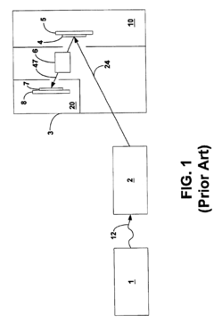
- Mask and reticle defect management: EUV masks present unique challenges due to their reflective nature and the absence of pellicles in early EUV systems. Technical issues include defect detection at nanometer scales, repair methodologies for mask defects, pattern fidelity maintenance, and handling multilayer reflective masks without introducing contamination. Advanced inspection tools and processes are required to identify and address both substrate and pattern defects that could impact final wafer quality.
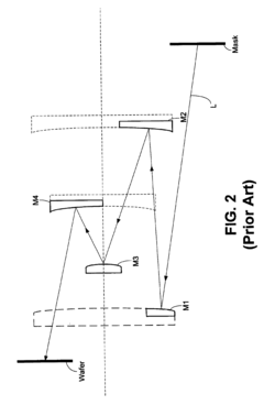
- Optics and mirror technology: EUV lithography relies on complex reflective optics instead of traditional transmissive lenses. Technical challenges include manufacturing ultra-precise aspheric mirrors with surface roughness below 0.1nm, maintaining mirror reflectivity over time, addressing thermal management issues caused by absorbed EUV radiation, and compensating for mirror distortions during operation. Multilayer coating technology must also be optimized to achieve maximum reflectivity at the 13.5nm wavelength.
- Photoresist and pattern development: EUV photoresist technology faces challenges including limited sensitivity requiring trade-offs between exposure dose, resolution, and line-edge roughness. The stochastic effects at sub-10nm resolution create variability in pattern formation due to the limited number of photons and chemical reactions involved. Additionally, outgassing from resists can contaminate the optical system, while achieving sufficient etch resistance with thin resist films presents further complications for pattern transfer processes.
- System integration and contamination control: EUV lithography systems require sophisticated vacuum environments and contamination control strategies. Challenges include maintaining vacuum integrity throughout the system, preventing carbon growth on optical surfaces from residual hydrocarbons, managing tin debris from plasma sources, and implementing effective contamination barriers. Additionally, system integration must address complex alignment requirements, thermal management across the tool, and advanced metrology for process control at extreme dimensions.
02 Mask defects and inspection issues
EUV masks present unique challenges due to their reflective nature and multilayer structure. Key issues include defect prevention, detection, and repair in both the absorber layer and the multilayer reflector. The absence of pellicles in early EUV systems increases contamination risks. Advanced inspection techniques are needed to identify pattern defects, phase defects, and particles that can significantly impact image quality and yield.Expand Specific Solutions03 Optical system and projection challenges
EUV optical systems rely on complex reflective optics rather than traditional refractive lenses. These systems face challenges including mirror surface accuracy, multilayer coating uniformity, thermal management, and minimizing wavefront errors. The projection optics must maintain extreme precision while handling the thermal load from EUV radiation. Achieving and maintaining the required optical performance is critical for resolution, overlay accuracy, and pattern fidelity.Expand Specific Solutions04 Photoresist and pattern development challenges
EUV photoresist technology faces fundamental challenges due to the high-energy photons and low photon count of EUV radiation. Key issues include achieving sufficient sensitivity while maintaining resolution, line edge roughness, and pattern collapse resistance. The stochastic effects become more pronounced at smaller feature sizes, leading to increased variability. Advanced development processes and materials are needed to meet the demanding requirements of EUV lithography.Expand Specific Solutions05 System integration and contamination control
EUV lithography systems require sophisticated integration of vacuum systems, contamination control, and thermal management. Molecular contamination can degrade mirror reflectivity and mask performance, while particulate contamination directly impacts yield. Maintaining the vacuum environment while enabling high throughput operation presents significant engineering challenges. Advanced sensors, control systems, and predictive maintenance are essential for stable operation and maximizing system availability.Expand Specific Solutions
Leading Companies and Research Institutions in EUV Ecosystem
EUV lithography is currently in a critical growth phase, with the market expanding rapidly despite significant technical challenges. The industry faces issues in power source efficiency, mask defects, and resist sensitivity, which are being addressed by key players. ASML Netherlands BV dominates the EUV equipment market, while Intel, TSMC, and Samsung lead in implementation. Companies like Carl Zeiss SMT focus on specialized optics, and Lam Research and Tokyo Electron develop complementary processes. The technology is approaching maturity for leading-edge nodes, but challenges remain in cost reduction and throughput improvement, with collaborative efforts across the ecosystem driving innovation in this complex field.
Taiwan Semiconductor Manufacturing Co., Ltd.
Technical Solution: TSMC has pioneered EUV implementation in high-volume manufacturing, beginning with their 7nm+ process and expanding to 5nm and 3nm nodes. Their approach to EUV technical challenges includes: (1) Development of specialized resist materials optimized for EUV sensitivity and line edge roughness reduction; (2) Advanced pellicle solutions that maintain high transmissivity while protecting masks from contamination; (3) Proprietary computational lithography techniques that address stochastic effects through design-technology co-optimization; (4) Multi-patterning strategies that combine EUV with traditional immersion lithography to optimize cost and performance; (5) Custom metrology systems for defect inspection and process control specific to EUV layers. TSMC has reported achieving sub-20nm pitch patterning with single-exposure EUV and has developed techniques to manage the increased mask complexity and defectivity challenges inherent to EUV processes.
Strengths: Industry-leading implementation experience across multiple technology nodes; extensive process integration knowledge; advanced computational lithography capabilities; strong financial position to invest in EUV infrastructure. Weaknesses: Dependency on ASML for EUV equipment; ongoing challenges with cost-per-layer economics; stochastic defect management still requiring redundant design approaches; limited EUV layer implementation compared to total process layers.
SAMSUNG SDI CO LTD
Technical Solution: Samsung has developed a comprehensive approach to EUV lithography implementation focusing on both hardware and process integration challenges. Their technical solutions include: (1) Custom-designed EUV mask infrastructure with advanced absorber materials that reduce shadowing effects and improve image contrast; (2) Proprietary resist formulations optimized for sensitivity and line edge roughness control, developed in partnership with specialized chemical suppliers; (3) Advanced computational lithography techniques including source-mask optimization and optical proximity correction specifically calibrated for EUV-specific effects; (4) Novel pellicle technologies that maintain high transmissivity while protecting masks from contamination; (5) Integration of machine learning algorithms for defect classification and process control specific to EUV layers. Samsung has implemented EUV in high-volume manufacturing for their 7nm process and beyond, and has reported achieving sub-20nm pitch patterning with single-exposure EUV techniques. Their approach includes strategic layer selection for EUV application to optimize cost-performance balance.
Strengths: Vertical integration allowing coordinated development across materials, process, and design; significant manufacturing scale enabling rapid learning cycles; strong financial position supporting continued EUV investment; advanced computational capabilities for process optimization. Weaknesses: Relatively later adoption compared to TSMC; ongoing challenges with stochastic defects requiring redundant design approaches; dependency on ASML for equipment; cost management pressures in competitive memory markets where margins are tighter.
Critical Patents and Innovations in EUV Lithography
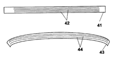
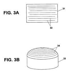
Method to avoid striae in EUV lithography mirrors
PatentInactiveUS6776006B2
Innovation
- The method involves sagging a plate of glass material to produce a mirror blank, where the striae planes remain parallel to the curved surface, minimizing the need for extensive grinding and polishing, and combining this with annealing techniques to attach a thin plate over a mirror base, ensuring only minor adjustments are needed to achieve the desired mirror shape and finish.
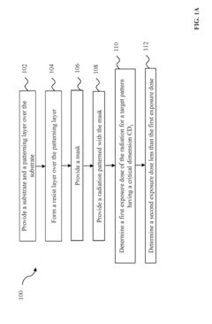
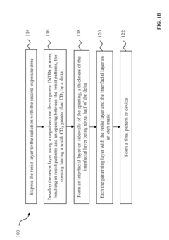
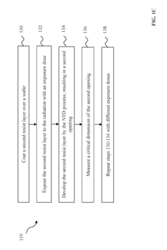
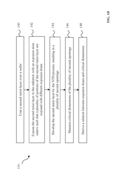
Extreme Ultraviolet Lithography with Reduced Exposure Dose and Negative Tone Development
PatentActiveUS20170315447A1
Innovation
- A two-step approach using a reduced EUV exposure dose followed by negative-tone development (NTD) and a shrinking process to achieve target critical dimensions while reducing LER and LWR, without increasing radiation power or resist sensitivity, utilizing existing EUV equipment and resists.
Supply Chain Vulnerabilities in EUV Equipment Manufacturing
The EUV lithography equipment supply chain represents one of the most complex and vulnerable technological ecosystems in the semiconductor industry. ASML's near-monopoly on EUV lithography systems creates a critical single point of failure in the global semiconductor manufacturing infrastructure. This Dutch company relies on a sophisticated network of over 5,000 suppliers across three continents, with approximately 800 core suppliers providing essential components and subsystems.
The extreme precision required for EUV systems magnifies supply chain vulnerabilities. Key components such as the laser-produced plasma source, ultra-precise mirrors with atomic-level smoothness, and specialized photoresist materials are produced by only a handful of companies worldwide. For instance, Zeiss in Germany is the sole supplier of the crucial optical systems, while Cymer (now an ASML subsidiary) provides the specialized light sources.
Geopolitical tensions have exposed significant risks in this supply chain. Export controls and trade restrictions between major economies like the US, China, and Europe have created uncertainty about access to critical components. The COVID-19 pandemic further revealed the fragility of this global supply network, with disruptions causing delays in EUV system deliveries and contributing to the ongoing semiconductor shortage.
Raw material constraints present another vulnerability layer. EUV systems require specialized materials including high-purity gases, rare earth elements, and ultra-pure silicon. Many of these materials face concentration risk, with production limited to specific geographic regions subject to political instability or export restrictions.
The knowledge-intensive nature of EUV manufacturing compounds these vulnerabilities. The technology requires highly specialized expertise in fields ranging from plasma physics to precision optics. This human capital dependency creates bottlenecks that cannot be quickly resolved through conventional supply chain management approaches.
Manufacturing capacity limitations also create vulnerabilities. ASML can only produce a limited number of EUV systems annually (approximately 40-50 units), creating competition among semiconductor manufacturers for access to these critical tools. This capacity constraint is exacerbated by the long lead times required for EUV system production, typically 12-18 months from order to delivery.
Addressing these vulnerabilities requires multi-faceted approaches including supply chain diversification, strategic stockpiling of critical components, development of alternative technologies, and international cooperation frameworks to ensure continued access to this essential technology despite geopolitical tensions.
Environmental and Safety Considerations in EUV Deployment
The deployment of Extreme Ultraviolet (EUV) lithography technology introduces significant environmental and safety considerations that must be addressed for successful implementation. EUV systems operate with high-power laser-produced plasma sources that generate 13.5nm wavelength radiation, creating unique workplace hazards. The primary concern involves radiation exposure risks to personnel, as EUV radiation can cause tissue damage and long-term health effects if proper shielding and safety protocols are not implemented.
Chemical safety represents another critical consideration in EUV deployment. The process utilizes various hazardous materials, including tin droplets for plasma generation and specialized photoresists containing potentially toxic compounds. These substances require comprehensive handling protocols, specialized disposal procedures, and emergency response plans to mitigate risks of chemical exposure or accidental release.
Energy consumption poses both environmental and operational challenges for EUV lithography. Current EUV systems demand extraordinary power requirements—typically 20-40 kW per tool—significantly exceeding those of previous lithography technologies. This intensive energy consumption contributes to increased carbon footprints and operational costs, prompting semiconductor manufacturers to invest in energy efficiency measures and renewable energy sources to offset environmental impacts.
Waste management presents ongoing challenges throughout the EUV lithography lifecycle. The technology generates various waste streams, including used photoresist materials, contaminated components, and tin debris from the plasma source. These materials often require specialized treatment before disposal due to their potential environmental persistence and toxicity profiles. Leading manufacturers have developed closed-loop recycling systems for certain materials, particularly tin recovery systems that minimize waste generation.
Thermal management constitutes a significant engineering challenge with environmental implications. EUV systems generate substantial heat that must be dissipated through advanced cooling systems, typically requiring large volumes of ultra-pure water and specialized temperature control infrastructure. The water usage and associated treatment processes represent additional environmental considerations that facilities must address through water recycling and conservation measures.
Regulatory compliance frameworks for EUV deployment vary globally but generally include occupational safety standards, environmental permits, and waste handling certifications. Organizations implementing EUV technology must navigate complex regulatory landscapes that continue to evolve as understanding of the technology's environmental impacts develops. Industry leaders have established collaborative initiatives to develop best practices and standardized approaches to environmental and safety management for EUV lithography.
Unlock deeper insights with PatSnap Eureka Quick Research — get a full tech report to explore trends and direct your research. Try now!
Generate Your Research Report Instantly with AI Agent
Supercharge your innovation with PatSnap Eureka AI Agent Platform!