

What Is the Future Trajectory for EUV Lithography Deployment
OCT 14, 20259 MIN READ
Generate Your Research Report Instantly with AI Agent
PatSnap Eureka helps you evaluate technical feasibility & market potential.
EUV Lithography Evolution and Objectives
Extreme Ultraviolet (EUV) lithography represents a revolutionary advancement in semiconductor manufacturing technology, marking a significant departure from traditional deep ultraviolet (DUV) lithography methods. The evolution of EUV technology began in the 1990s when semiconductor industry leaders recognized the approaching physical limitations of conventional optical lithography techniques. As transistor dimensions continued to shrink according to Moore's Law, the industry faced critical challenges in achieving higher resolution patterns with existing 193nm immersion lithography.
The development trajectory of EUV lithography has been characterized by persistent engineering challenges and collaborative industry efforts. Initial research focused on generating and controlling 13.5nm wavelength light, requiring significant innovations in light source technology, optics, and photoresist chemistry. By the early 2000s, ASML, in partnership with Zeiss, began developing the first EUV lithography prototypes, while companies like Cymer (later acquired by ASML) worked on high-power EUV light sources.
A critical milestone occurred in 2016-2017 when ASML delivered the first commercial EUV lithography systems capable of high-volume manufacturing. The NXE:3400B system represented the culmination of decades of research and billions of dollars in investment, enabling 7nm node semiconductor production. This achievement fundamentally altered the semiconductor manufacturing landscape, allowing continued miniaturization beyond what was possible with DUV technology.
The primary objective of EUV lithography deployment is to enable semiconductor manufacturers to continue scaling according to Moore's Law while managing economic constraints. With a wavelength of 13.5nm (compared to 193nm for DUV), EUV technology theoretically allows for significantly smaller feature sizes without requiring complex multi-patterning techniques that increase manufacturing costs and complexity.
Current technical objectives for EUV lithography include increasing throughput (wafers per hour), improving power efficiency, enhancing resolution capabilities, and reducing defectivity rates. The industry aims to achieve high-volume manufacturing capability at increasingly advanced nodes (5nm, 3nm, and beyond) while simultaneously reducing the cost per transistor to maintain economic viability.
Looking forward, the EUV roadmap includes the development of high-NA (numerical aperture) EUV systems, which promise to extend resolution capabilities even further. ASML's EXE:5000 system, with a numerical aperture of 0.55 (compared to 0.33 in current systems), represents the next generation of EUV technology aimed at enabling 2nm node production and beyond. This evolution underscores the industry's commitment to maintaining the pace of semiconductor advancement despite growing technical and economic challenges.
Semiconductor Industry Demand Analysis
The semiconductor industry's demand for advanced lithography technologies, particularly EUV (Extreme Ultraviolet) lithography, is primarily driven by the continuous pursuit of Moore's Law and the need for increasingly powerful and energy-efficient computing solutions. As transistor dimensions continue to shrink below 7nm, traditional DUV (Deep Ultraviolet) lithography faces fundamental physical limitations, making EUV technology essential for future semiconductor manufacturing.
Market analysis indicates that the global semiconductor industry is projected to reach $1 trillion by 2030, with advanced nodes requiring EUV technology representing a significant growth segment. The demand is particularly strong in high-performance computing, artificial intelligence, 5G/6G telecommunications, and autonomous systems sectors, where computational density and power efficiency are critical competitive factors.
The adoption of EUV lithography is accelerating across major semiconductor manufacturers. TSMC, Samsung, and Intel have all made substantial investments in EUV equipment for their leading-edge process nodes. TSMC's capital expenditure for advanced lithography exceeded $30 billion in 2022, with a significant portion allocated to EUV systems. Similarly, Samsung has committed $116 billion to its semiconductor roadmap through 2030, heavily emphasizing EUV technology.
Geographic demand patterns show concentration in East Asia, particularly Taiwan and South Korea, where the majority of advanced semiconductor manufacturing occurs. However, recent geopolitical tensions and supply chain vulnerabilities have prompted initiatives like the CHIPS Act in the United States and similar programs in Europe, potentially diversifying the geographic distribution of EUV deployment in the coming decade.
The demand for EUV lithography is further intensified by emerging applications in quantum computing, neuromorphic chips, and advanced packaging technologies. These next-generation computing paradigms require unprecedented precision in semiconductor manufacturing, which only EUV can provide at economically viable yields.
Customer segments for EUV technology include pure-play foundries (42% of market demand), integrated device manufacturers (35%), and memory manufacturers (23%). The memory segment is expected to increase its share as EUV becomes more critical for advanced DRAM and NAND production, potentially reaching 30% by 2025.
Industry forecasts suggest that annual EUV system installations will grow from approximately 100 units in 2023 to over 200 units by 2027, representing a compound annual growth rate of 18.9%. This growth trajectory is supported by the expanding application scope of EUV technology beyond logic chips to include high-bandwidth memory, advanced sensors, and specialized processors for AI acceleration.
Global EUV Technology Landscape and Barriers
The global landscape of Extreme Ultraviolet (EUV) lithography technology presents a complex picture of concentrated innovation centers and significant technical barriers. Currently, the EUV ecosystem is dominated by a small number of key players, with ASML (Netherlands) holding a virtual monopoly on EUV lithography machine production. This concentration creates both technological advantages through focused R&D and potential vulnerabilities in the global semiconductor supply chain.
Geographically, EUV technology development is primarily centered in advanced semiconductor manufacturing regions: Western Europe (particularly the Netherlands), East Asia (Japan, South Korea, Taiwan), and North America (United States). Each region contributes different components to the EUV ecosystem, with specialized expertise in areas such as light sources, optics, photoresist chemistry, and integration systems.
Despite significant progress, EUV lithography faces several critical technical barriers. Power source stability remains a fundamental challenge, as current EUV systems operate at 13.5nm wavelength requiring sophisticated laser-produced plasma technology that struggles with consistent power output. This directly impacts throughput and economic viability for mass production scenarios.
Mask defectivity presents another significant hurdle. The complexity of manufacturing defect-free EUV masks is exponentially higher than for traditional lithography, with even nanoscale imperfections causing critical pattern failures. Current inspection and repair technologies struggle to keep pace with increasingly stringent requirements for advanced nodes.
Photoresist performance constitutes a third major barrier. The interaction between EUV photons and resist materials differs fundamentally from traditional lithography, requiring novel chemistries that simultaneously deliver high resolution, low line edge roughness, and sufficient sensitivity—a challenging combination known as the "RLS trade-off."
Infrastructure requirements also limit global deployment. EUV systems demand extraordinary environmental stability, including vibration isolation, temperature control to millikelvin precision, and vacuum systems of exceptional quality. These requirements translate to fabrication facilities costing billions of dollars, restricting adoption to only the most advanced semiconductor manufacturers.
Talent availability represents a less discussed but equally critical barrier. The highly specialized knowledge required for EUV technology development and operation has created a global shortage of qualified engineers and technicians, further constraining expansion beyond current centers of excellence.
Current EUV Implementation Strategies
01 EUV lithography system development and optimization
Development and optimization of EUV lithography systems focus on improving the efficiency and performance of the lithography process. This includes advancements in optical systems, light sources, and overall system architecture to enhance resolution and throughput. Various techniques are employed to optimize the exposure process, reduce defects, and improve pattern transfer accuracy, enabling the production of smaller and more complex semiconductor devices.- EUV lithography system development and optimization: The development and optimization of EUV lithography systems focus on improving the efficiency and performance of the lithography process. This includes advancements in optical systems, illumination sources, and overall system architecture to enhance resolution and throughput. Various techniques are employed to optimize the exposure process, reduce defects, and improve pattern fidelity, contributing to the evolution and deployment trajectory of EUV lithography technology.
- EUV source technology and power scaling: EUV source technology has been a critical factor in the deployment trajectory of EUV lithography. Innovations focus on developing high-power, stable EUV light sources, primarily based on laser-produced plasma or discharge-produced plasma. These advancements address challenges related to source power, stability, and reliability, which have been key bottlenecks in the widespread adoption of EUV lithography in semiconductor manufacturing.
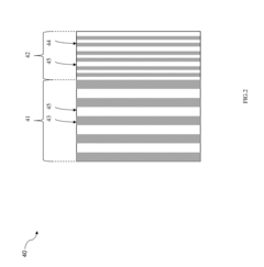
- Mask technology and defect management: Mask technology plays a crucial role in the deployment of EUV lithography. Innovations in this area focus on developing defect-free masks, inspection techniques, and repair methodologies. Managing mask defects is particularly challenging in EUV lithography due to the reflective nature of EUV masks and the absence of pellicles in early implementations. Advancements in mask technology have been essential for enabling the commercial viability of EUV lithography.
- Integration with semiconductor manufacturing processes: The integration of EUV lithography into existing semiconductor manufacturing processes has been a significant aspect of its deployment trajectory. This includes developing compatible resists, optimizing process flows, and ensuring seamless integration with other manufacturing steps. The transition from traditional optical lithography to EUV lithography requires substantial modifications to the overall manufacturing ecosystem, including changes to design rules, metrology, and process control strategies.
- Economic and technological roadmap considerations: The deployment trajectory of EUV lithography has been significantly influenced by economic factors and technological roadmap considerations. This includes cost-benefit analyses, timing of introduction relative to semiconductor node transitions, and alignment with industry roadmaps. The high cost of EUV lithography tools and infrastructure has necessitated careful planning for their introduction, with initial deployment targeting critical layers in advanced nodes before expanding to broader applications as the technology matures and costs decrease.
02 EUV source technology and power scaling
EUV source technology is critical for lithography deployment, with significant focus on increasing source power for improved throughput. Innovations include laser-produced plasma sources, discharge-produced plasma, and methods to enhance conversion efficiency. Power scaling solutions address challenges in source stability, debris mitigation, and collector optics lifetime, which are essential for commercial viability of EUV lithography in high-volume manufacturing environments.Expand Specific Solutions03 Mask technology and defect management
Mask technology for EUV lithography involves specialized reflective masks rather than traditional transmissive ones. Innovations focus on multilayer reflective coatings, absorber materials, and phase-shifting techniques to enhance pattern fidelity. Defect management strategies include advanced inspection methods, repair techniques, and compensation algorithms to address the unique challenges of EUV masks, such as three-dimensional effects and pattern-dependent variations that impact the final image quality.Expand Specific Solutions04 Integration with semiconductor manufacturing processes
Integration of EUV lithography into existing semiconductor manufacturing processes requires significant adaptations to workflow, materials, and equipment. This includes development of compatible photoresists with high sensitivity and resolution, process control methods, and alignment strategies. The deployment trajectory involves phased introduction of EUV for critical layers while maintaining compatibility with other lithography techniques for non-critical layers, enabling a smooth transition to advanced node production.Expand Specific Solutions05 Economic and technological roadmap for EUV adoption
The economic and technological roadmap for EUV adoption considers cost-benefit analysis, timing of deployment, and strategic implementation across different semiconductor device generations. Factors influencing the deployment trajectory include system cost, throughput capabilities, yield improvements, and competitive advantages gained from smaller feature sizes. The roadmap also addresses infrastructure requirements, workforce training, and supply chain development necessary for successful industry-wide implementation of EUV lithography technology.Expand Specific Solutions
Leading EUV Equipment Manufacturers and Ecosystem
EUV lithography is entering a mature deployment phase, with market size expected to grow significantly as semiconductor manufacturers transition to advanced nodes. The technology has reached commercial viability after decades of development, with ASML Netherlands BV maintaining dominant market position as the sole EUV lithography system supplier. Key semiconductor manufacturers like Taiwan Semiconductor Manufacturing Co., Intel, and Samsung Electronics are driving adoption through significant investments. Supporting ecosystem players including Carl Zeiss SMT (optical components), AGC and Shin-Etsu Chemical (materials), and Nikon (competing technologies) are establishing their positions. Chinese entities like Shanghai Micro Electronics Equipment and Institute of Microelectronics are working to develop domestic alternatives, though they remain years behind the technological frontier.
Taiwan Semiconductor Manufacturing Co., Ltd.
Technical Solution: TSMC has been at the forefront of EUV lithography implementation in high-volume manufacturing. The company began its EUV journey with the 7nm N7+ process in 2019 and has progressively increased EUV layer usage in subsequent nodes. For their 5nm process, TSMC employs up to 14 EUV layers, while their 3nm process (N3) utilizes over 20 EUV layers. TSMC has developed a comprehensive EUV infrastructure including specialized clean rooms, advanced mask preparation facilities, and proprietary process recipes that optimize EUV performance. Their approach includes custom computational lithography solutions that enhance resolution and pattern fidelity through source mask optimization and optical proximity correction techniques specifically tailored for EUV. TSMC has also pioneered EUV-specific design rules and methodologies to maximize yield and performance. The company's future roadmap includes plans for implementing High-NA EUV for their 2nm node and beyond, with significant investments in both equipment and process development to support this transition.
Strengths: Industry-leading implementation experience with EUV in high-volume manufacturing; sophisticated process integration capabilities; strong financial position to continue investing in advanced EUV tools; established design ecosystem supporting EUV-based nodes. Weaknesses: Dependency on ASML as the sole EUV equipment supplier; increasing technical challenges as feature sizes approach fundamental physical limits; high capital expenditure requirements for maintaining technology leadership.
Carl Zeiss SMT GmbH
Technical Solution: Zeiss SMT has established itself as the critical supplier of EUV optical systems, developing and manufacturing the complex projection optics and illumination systems that form the heart of ASML's EUV lithography tools. Their technology includes precision-engineered mirror systems with surface accuracy requirements measured in atomic dimensions - less than 50 picometers of deviation. For High-NA EUV systems, Zeiss has developed an innovative optical design featuring a central obscuration and anamorphic projection that enables the 0.55 numerical aperture while managing the increased complexity of the larger optical path. Their manufacturing process involves proprietary ion beam figuring techniques and metrology systems capable of measuring surface accuracies beyond what was previously possible. Zeiss has also developed specialized coating technologies for the multilayer reflective surfaces required for EUV wavelengths, achieving reflectivity levels that make commercial EUV lithography viable. Their Starlith® optical systems incorporate active compensation mechanisms that maintain critical dimensions despite thermal and mechanical stresses during operation.
Strengths: Unmatched expertise in EUV optics design and manufacturing; proprietary metrology capabilities for ultra-precise measurements; established partnership with ASML ensuring market access; continuous innovation pipeline for optical performance improvements. Weaknesses: Extreme manufacturing complexity limiting production capacity; dependency on specialized materials and processes with limited supplier options; challenges in scaling production to meet increasing industry demand; high sensitivity of optical performance to manufacturing variations.
Critical Patents and Breakthroughs in EUV Technology
Extreme Ultraviolet Lithography Process and Mask
PatentActiveUS20150168845A1
Innovation
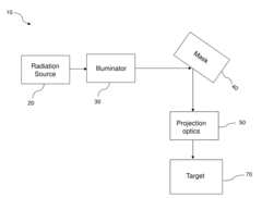
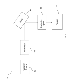
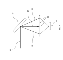
- The implementation of a nearly on-axis illumination with partial coherence less than 0.3 in an EUV lithography system, combined with an EUV mask featuring a first region with main polygons and a second region with sub-resolution polygons, and a spatial filter to remove most non-diffracted light, enhancing spatial frequency resolution and uniformity of exposure intensity.
EUV Lithography System With 3D Sensing and Tunning Modules
PatentPendingUS20240103378A1
Innovation
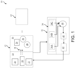
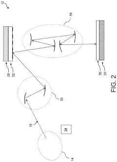
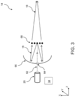
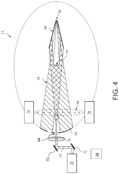
- An EUV lithography system integrated with a 3D diagnostic module and control system that monitors and analyzes laser beam, plasma, and EUV radiation parameters, using correlation analysis, machine learning, and real-time tuning to optimize the lithography process, reducing debris and enhancing EUV radiation energy.
Supply Chain Resilience for EUV Components
The EUV lithography supply chain represents one of the most complex and concentrated technological ecosystems in the semiconductor industry. ASML's near-monopoly on EUV lithography systems creates an inherent vulnerability, as any disruption to their operations could have cascading effects throughout the global semiconductor manufacturing landscape. This concentration risk is further compounded by the specialized nature of critical components, with only a handful of suppliers capable of meeting the extreme precision requirements for EUV mirrors, lasers, and optical systems.
Geographic concentration presents another significant challenge, with key suppliers clustered primarily in Europe, Japan, and the United States. Recent geopolitical tensions and export control measures have highlighted the fragility of this arrangement, particularly as semiconductor manufacturing increasingly becomes intertwined with national security interests. The COVID-19 pandemic further exposed vulnerabilities when border closures and workforce limitations created bottlenecks in component delivery and system installation.
Raw material dependencies also pose substantial risks to supply chain resilience. EUV systems require specialized materials including high-purity gases, rare earth elements, and ultra-pure silicon. Many of these materials face potential supply constraints due to limited global sources, environmental regulations affecting extraction, or geopolitical factors controlling access to deposits.
To address these vulnerabilities, leading semiconductor manufacturers are implementing multi-faceted resilience strategies. Strategic inventory management has become increasingly important, with companies maintaining larger stockpiles of critical components despite the associated capital costs. Diversification efforts are also underway, with manufacturers encouraging the development of alternative suppliers for previously single-sourced components.
Vertical integration represents another approach, with some major semiconductor players investing in or acquiring suppliers of critical EUV components to ensure prioritized access. Collaborative industry initiatives are also emerging, including joint investment in supply chain monitoring technologies and shared contingency planning for potential disruptions.
Looking forward, the industry is exploring advanced manufacturing techniques that could reduce dependency on specific materials or components. Additive manufacturing shows promise for certain specialized parts, potentially enabling more distributed production capabilities. Additionally, design innovations that standardize certain components across multiple EUV system generations could help reduce supply chain complexity and improve resilience against future disruptions.
Environmental Impact of EUV Manufacturing Processes
The environmental footprint of Extreme Ultraviolet (EUV) lithography represents a critical consideration as this technology continues its deployment trajectory across the semiconductor industry. EUV systems consume substantial energy, with a single lithography tool requiring between 500-1000 kW during operation—significantly higher than previous generation Deep Ultraviolet (DUV) systems. This increased power demand stems primarily from the complex laser-produced plasma process needed to generate EUV light, where tin droplets are vaporized by high-powered CO2 lasers.
Water usage presents another significant environmental challenge. EUV systems require ultra-pure water for cooling and cleaning processes, with consumption rates estimated at 300-600 liters per hour during peak operation. This places considerable strain on local water resources, particularly in semiconductor manufacturing hubs already experiencing water scarcity issues such as Taiwan and parts of the southwestern United States.
The production of EUV equipment involves rare earth elements and specialized materials whose mining and refinement carry substantial environmental consequences. The manufacturing of precision optics, particularly the multi-layer mirrors essential to EUV systems, requires materials like ruthenium and molybdenum that have environmentally intensive extraction processes.
Chemical usage in EUV processes, while more efficient per wafer than previous technologies, still involves photoresists and development chemicals that require careful handling and disposal. Industry data suggests that while chemical consumption per transistor has decreased, the absolute volume continues to grow as production scales.
Several mitigation strategies are emerging within the industry. Leading manufacturers like ASML and their customers have begun implementing closed-loop water recycling systems that can reduce freshwater consumption by up to 60%. Energy efficiency improvements focus on optimizing the conversion efficiency of CO2 lasers and reducing idle power consumption through advanced power management systems.
Carbon footprint reduction initiatives are gaining traction, with major semiconductor manufacturers committing to renewable energy transitions for their fabs. Intel, TSMC, and Samsung have all announced plans to significantly increase renewable energy usage in their operations by 2030, directly addressing the carbon impact of EUV deployment.
Looking forward, the industry faces the challenge of balancing technological advancement with environmental sustainability. Next-generation High-NA EUV systems promise greater efficiency per wafer but may initially increase absolute resource consumption. The development of more environmentally benign photoresists and processing chemicals represents another promising research direction that could significantly reduce the ecological impact of EUV manufacturing processes.
Unlock deeper insights with PatSnap Eureka Quick Research — get a full tech report to explore trends and direct your research. Try now!
Generate Your Research Report Instantly with AI Agent
Supercharge your innovation with PatSnap Eureka AI Agent Platform!