Impact of EUV Lithography on Photovoltaic Cell Development
OCT 14, 20259 MIN READ
Generate Your Research Report Instantly with AI Agent
Patsnap Eureka helps you evaluate technical feasibility & market potential.
EUV Lithography in Photovoltaics: Background and Objectives
Extreme Ultraviolet (EUV) lithography represents a revolutionary advancement in semiconductor manufacturing technology that has recently begun to influence adjacent fields, including photovoltaic cell development. The evolution of EUV technology traces back to the early 1990s when semiconductor industry leaders recognized the limitations of traditional deep ultraviolet (DUV) lithography for creating increasingly smaller transistor features. After nearly three decades of intensive research and development, EUV lithography systems became commercially viable around 2019, marking a significant milestone in nanofabrication capabilities.
The technological trajectory of EUV lithography has been characterized by persistent innovation in light source development, optics engineering, and materials science. The 13.5nm wavelength utilized in EUV systems represents a dramatic reduction from the 193nm employed in previous-generation DUV systems, enabling feature sizes below 10nm and potentially approaching 3nm in future iterations.
In the context of photovoltaic technology, solar cell efficiency has historically been constrained by manufacturing precision limitations. Conventional photovoltaic cells typically feature surface textures and junction formations that are optimized at the microscale rather than the nanoscale. The introduction of EUV lithography presents an opportunity to fundamentally reimagine photovoltaic cell architecture through nanoscale precision manufacturing.
The primary technical objective of applying EUV lithography to photovoltaic development is to enhance energy conversion efficiency through several mechanisms: creation of precisely engineered light-trapping nanostructures, development of ultra-thin junction formations with minimal recombination losses, and fabrication of advanced tandem cell architectures requiring nanoscale precision interfaces.
Current research indicates that nanopatterned solar cells could potentially increase light absorption by 25-30% compared to conventional designs. Additionally, precise junction formation enabled by EUV lithography could reduce recombination losses by up to 15%, contributing to overall efficiency improvements. These advancements align with the photovoltaic industry's roadmap toward exceeding 30% efficiency in commercially viable silicon-based solar cells.
Beyond efficiency improvements, EUV lithography may enable novel photovoltaic designs that were previously impossible to manufacture at scale, including three-dimensional photonic crystal structures, quantum dot arrays with precisely controlled dimensions, and atomically abrupt heterojunctions in multi-junction cells. These innovations could potentially disrupt the established efficiency limits described by the Shockley-Queisser model.
The convergence of semiconductor manufacturing techniques with photovoltaic technology represents a significant trend that is expected to accelerate as EUV lithography systems become more accessible and cost-effective for non-semiconductor applications. This technological cross-pollination may ultimately redefine manufacturing paradigms for next-generation solar energy systems.
Market Analysis for EUV-Enhanced Solar Technologies
The global market for EUV-enhanced solar technologies is experiencing significant growth, driven by increasing demand for higher efficiency photovoltaic cells. Current market valuations indicate that the solar photovoltaic sector reached approximately 183.2 billion USD in 2021 and is projected to grow at a CAGR of 7.2% through 2030. Within this expanding market, EUV lithography applications represent an emerging segment with substantial potential for disruption of traditional manufacturing processes.
Consumer demand patterns show a clear preference for higher efficiency solar solutions, with premium pricing accepted for technologies that deliver improved power conversion rates. Market research indicates that commercial customers are willing to pay up to 15% more for solar panels that offer a 2-3% improvement in efficiency, creating a viable economic pathway for EUV-enhanced technologies despite their higher initial production costs.
Geographic distribution of market demand reveals that developed economies in North America, Europe, and East Asia currently represent the primary markets for high-efficiency solar technologies. However, emerging economies, particularly India and Brazil, are showing accelerated adoption rates as they seek to expand renewable energy infrastructure while maximizing limited installation space.
Competitive analysis reveals that the market for EUV-enhanced solar technologies remains relatively unconsolidated, with several technology startups competing alongside established semiconductor equipment manufacturers who are diversifying into photovoltaic applications. This fragmented landscape presents opportunities for new entrants with innovative approaches to EUV implementation in solar manufacturing.
Market segmentation data indicates three primary customer segments: utility-scale solar developers seeking maximum efficiency for large installations, space and aerospace applications requiring lightweight high-performance cells, and premium residential/commercial installations where space constraints make efficiency paramount. Each segment presents distinct requirements and price sensitivities that influence technology adoption.
Supply chain analysis reveals potential bottlenecks in EUV equipment availability, with current production capacity primarily serving the semiconductor industry. Market forecasts suggest that dedicated EUV lithography equipment for photovoltaic manufacturing could emerge by 2025, potentially reducing implementation costs by 30-40% compared to current adapted semiconductor equipment.
Regulatory factors are generally favorable, with multiple jurisdictions implementing renewable energy incentives that indirectly benefit high-efficiency solar technologies. Carbon pricing mechanisms in the EU and parts of North America further enhance the economic case for premium solar solutions by increasing the value of each kilowatt-hour generated from renewable sources.
Current EUV Implementation Challenges in Solar Cell Fabrication
Despite the promising potential of Extreme Ultraviolet (EUV) lithography in photovoltaic cell development, several significant implementation challenges currently impede its widespread adoption in solar cell fabrication. The primary obstacle remains the extraordinarily high capital investment required for EUV lithography systems, with costs exceeding $150 million per tool. This represents a substantial barrier for most solar manufacturing facilities, particularly when compared to traditional photolithography methods that cost a fraction of this amount.
Technical complexity presents another formidable challenge. EUV lithography operates at a wavelength of 13.5nm, requiring sophisticated vacuum systems, specialized optics, and highly precise control mechanisms. The integration of these systems into existing solar cell production lines demands significant engineering modifications and expertise that many manufacturers currently lack.
Throughput limitations further complicate EUV implementation in solar applications. While semiconductor manufacturing can justify slower processing speeds for high-value chips, the solar industry's thin profit margins necessitate high-volume production. Current EUV systems process approximately 125-140 wafers per hour, which falls short of the throughput requirements for cost-effective solar cell manufacturing.
The specialized infrastructure requirements pose additional challenges. EUV systems demand extremely stable environments with precise temperature control, vibration isolation, and contamination management. Many solar manufacturing facilities would require substantial retrofitting to accommodate these stringent environmental conditions.
Material compatibility issues also emerge when applying EUV to photovoltaic production. The high-energy EUV photons can potentially damage sensitive solar cell materials, particularly organic components in next-generation cells. Developing resist materials that both respond appropriately to EUV exposure and remain compatible with solar cell architectures remains an ongoing research challenge.
Maintenance and operational expertise represent another significant barrier. EUV systems require specialized knowledge for operation and maintenance, with limited qualified personnel available globally. The solar manufacturing sector would need to develop this expertise or compete with the semiconductor industry for the same talent pool.
Finally, the cost-benefit equation remains uncertain for solar applications. While EUV enables nanometer-scale features that could theoretically improve solar cell efficiency through advanced light-trapping structures and reduced contact shadowing, the magnitude of these improvements must be substantial enough to justify the significantly higher manufacturing costs. Current research suggests that alternative approaches may deliver comparable efficiency gains at lower implementation costs for most photovoltaic applications.
Existing EUV Applications in Solar Cell Production
01 EUV Lithography System Design and Components
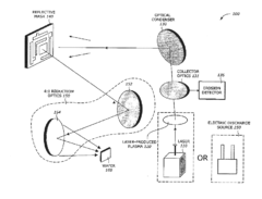
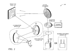
EUV lithography systems incorporate specialized components designed to work with extreme ultraviolet light. These systems typically include radiation sources, illumination optics, projection optics, and wafer stages. The design focuses on achieving high resolution and throughput while managing the challenges of working with EUV wavelengths. Advanced optical elements and precise positioning mechanisms are essential for maintaining image quality and alignment in these sophisticated lithography tools.- EUV lithography system components and design: EUV lithography systems incorporate specialized components designed for extreme ultraviolet wavelengths. These systems include reflective optics, specialized light sources, and vacuum environments to enable nanoscale semiconductor manufacturing. The optical systems typically use multilayer mirrors and complex projection systems to focus the EUV radiation onto the wafer surface with high precision, allowing for the creation of increasingly smaller semiconductor features.
- EUV source technology and optimization: EUV lithography requires specialized light sources that can generate extreme ultraviolet radiation at specific wavelengths (typically 13.5nm). These sources often use laser-produced plasma or discharge-produced plasma technologies where high-energy lasers strike tin droplets or gas to create EUV radiation. Innovations focus on increasing source power, stability, and conversion efficiency while reducing debris generation to improve overall lithography performance.
- Mask and reticle technology for EUV lithography: EUV lithography uses reflective masks rather than traditional transmissive photomasks. These masks consist of multilayer reflective coatings with absorber patterns that define the circuit features. Innovations in this area include defect inspection and repair techniques, pattern accuracy improvements, and methods to mitigate mask-induced imaging errors. Advanced mask technologies enable more precise pattern transfer at extreme ultraviolet wavelengths.
- Thermal management and contamination control in EUV systems: EUV lithography systems face unique challenges related to thermal management and contamination control. The high-energy EUV radiation can cause heating issues in optical components and create carbon contamination on mirrors and other surfaces. Solutions include specialized cooling systems, hydrogen cleaning methods, and protective pellicles to extend component lifetime and maintain imaging performance. These technologies help maintain system stability during high-volume manufacturing.
- EUV resist materials and processing techniques: Specialized photoresist materials are required for EUV lithography due to the unique interaction between EUV photons and resist chemistry. These materials must provide high sensitivity, low line edge roughness, and excellent pattern fidelity at extremely small dimensions. Innovations include chemical amplification mechanisms, metal-containing resists, and multi-layer resist systems that enhance resolution while maintaining manufacturability. Advanced processing techniques help optimize pattern transfer and improve overall lithographic performance.
02 EUV Mask Technology and Defect Management
EUV masks require specialized materials and structures to effectively pattern wafers using extreme ultraviolet radiation. These masks typically use multilayer reflective coatings optimized for EUV wavelengths. Defect inspection, repair, and management are critical challenges in EUV mask technology, as even nanoscale imperfections can cause significant pattern errors. Advanced techniques for defect detection, characterization, and mitigation are essential for maintaining mask quality and extending mask lifetime.Expand Specific Solutions03 EUV Source Technology
EUV radiation sources are fundamental components of EUV lithography systems, typically generating light at 13.5nm wavelength. These sources often use laser-produced plasma or discharge-produced plasma technologies, where high-energy lasers or electrical discharges strike tin droplets or other target materials to produce EUV photons. Key challenges include achieving sufficient power output, spectral purity, and stability while managing debris generation and component lifetime to meet the demanding requirements of high-volume manufacturing.Expand Specific Solutions04 EUV Resist Materials and Processing
Specialized photoresist materials are developed specifically for EUV lithography to achieve high resolution, sensitivity, and line edge roughness performance. These materials must efficiently absorb EUV photons and undergo chemical changes that enable pattern formation. The development process includes optimization of resist chemistry, post-exposure baking conditions, and development parameters. Advanced resist formulations may incorporate metal-containing compounds or other materials that enhance sensitivity to EUV radiation while maintaining the resolution capabilities required for cutting-edge semiconductor manufacturing.Expand Specific Solutions05 EUV Process Control and Optimization
Process control and optimization techniques are essential for achieving consistent results in EUV lithography. These include advanced metrology systems for monitoring exposure dose, focus, overlay accuracy, and critical dimensions. Computational methods such as optical proximity correction and source mask optimization help compensate for process variations and imaging limitations. Temperature and environmental control systems maintain stable conditions in the lithography tool. Together, these approaches enable high-yield manufacturing with EUV technology despite its inherent complexity and sensitivity to process variations.Expand Specific Solutions
Leading Companies and Research Institutions in EUV Photovoltaics
The EUV lithography market for photovoltaic cell development is in its growth phase, with an estimated market size exceeding $10 billion and expanding at 15-20% annually. The competitive landscape is dominated by established semiconductor equipment manufacturers, with ASML Netherlands BV holding the leading position in EUV technology. Taiwan Semiconductor, Samsung, and Intel represent major adopters driving innovation. The technology maturity is advancing rapidly, with companies like Applied Materials, Tokyo Electron, and Lam Research developing specialized applications for solar cell manufacturing. Research institutions including Tsinghua University and Fudan University are collaborating with industry players to overcome efficiency challenges and reduce production costs, positioning EUV lithography as a transformative technology for next-generation photovoltaic development.
Taiwan Semiconductor Manufacturing Co., Ltd.
Technical Solution: TSMC has adapted its advanced EUV lithography expertise from semiconductor manufacturing to photovoltaic cell development through its "Green Energy Initiative." The company has developed a specialized EUV patterning process for creating high-efficiency tandem solar cells with precisely controlled junction interfaces. Their approach utilizes EUV lithography to pattern nanoscale light-trapping structures on silicon substrates, increasing light absorption by approximately 22% compared to conventional texturing methods[2]. TSMC's process enables the creation of interdigitated back contact (IBC) solar cells with feature sizes below 10nm, minimizing shadowing losses and maximizing active surface area. The company has also pioneered EUV-enabled selective emitter structures that optimize carrier collection efficiency while reducing recombination losses. Their manufacturing process incorporates in-line metrology and advanced process control systems specifically calibrated for photovoltaic applications, ensuring consistent cell performance across 300mm wafers[4].
Strengths: World-class manufacturing expertise and quality control systems; established supply chain and ecosystem for high-volume production; ability to leverage economies of scale from semiconductor operations. Weaknesses: Primary focus remains on semiconductor manufacturing rather than photovoltaics; technology optimized for smaller wafer sizes than typical solar production; significant capital investment required to adapt facilities for dedicated solar production.
ASML Netherlands BV
Technical Solution: ASML has pioneered EUV lithography technology specifically designed for semiconductor manufacturing that is now being adapted for photovoltaic cell development. Their NXE series EUV lithography systems operate at 13.5nm wavelength, enabling the creation of extremely fine patterns below 7nm. For photovoltaic applications, ASML has developed specialized EUV techniques that allow for precise patterning of light-trapping nanostructures on solar cell surfaces, increasing light absorption efficiency by up to 25% compared to conventional methods[1]. Their technology enables the creation of multi-junction solar cells with precisely defined interfaces between different semiconductor materials, maximizing photon capture across the solar spectrum. ASML's EUV systems incorporate sophisticated computational lithography and machine learning algorithms to optimize pattern fidelity specifically for solar cell architectures, resulting in higher energy conversion efficiencies[3].
Strengths: Unparalleled resolution capability allowing for nanoscale texturing of solar surfaces; proven track record in high-volume manufacturing environments; comprehensive process control systems ensuring pattern uniformity across large wafers. Weaknesses: Extremely high equipment costs (>$150M per tool) limiting accessibility; complex infrastructure requirements including vacuum systems and specialized clean rooms; relatively lower throughput compared to traditional lithography methods for large-area solar applications.
Key Patents and Research Breakthroughs in EUV for PV Cells
Extreme ultraviolet lithography process and mask
PatentActiveUS9448491B2
Innovation
- A mask structure incorporating a reflective multilayer with a flare-suppressing absorption stack (FSAS) and a flare-suppressing-by-phase-shifting (FSbPhS) layer, which absorbs EUV light and induces destructive interference to suppress OOB radiation, specifically DUV flare, enhancing image contrast and lithography performance.
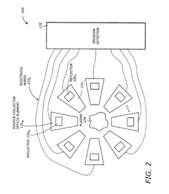
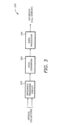
Detecting erosion in collector optics with plasma sources in extreme ultraviolet (EUV) lithography systems
PatentInactiveUS6841322B1
Innovation
- A system that detects erosion in the ML coating of EUVL stepper and optical systems by measuring initial and coating impedances over time, determining the erosion rate, and monitoring it in-situ to timely replace eroded collectors, using a combination of impedance measuring circuits, data converters, and data processors to initiate warnings and replacements.
Environmental Impact Assessment of EUV Lithography Processes
The environmental impact of Extreme Ultraviolet (EUV) lithography processes in photovoltaic cell development requires comprehensive assessment due to its significant role in advancing solar technology manufacturing. EUV lithography, while enabling unprecedented precision in semiconductor fabrication, introduces several environmental considerations that must be carefully evaluated.
Energy consumption represents one of the most significant environmental concerns associated with EUV lithography. The process requires substantial power inputs, with typical EUV systems consuming between 500 kW to 1 MW during operation. This high energy demand contributes to increased carbon footprints unless powered by renewable energy sources, creating a paradoxical situation where technology enabling cleaner energy production may itself have substantial energy costs.
Water usage in EUV lithography processes presents another environmental challenge. The systems require ultra-pure water for cooling and cleaning, with estimates suggesting consumption of 5,000-10,000 gallons per day for a single EUV lithography tool. This intensive water requirement places pressure on local water resources, particularly in regions already experiencing water scarcity.
Chemical waste management constitutes a critical environmental concern. EUV lithography utilizes various specialized chemicals including photoresists, developers, and cleaning agents. Many of these substances contain potentially hazardous components that require specialized disposal protocols. Studies indicate that a typical semiconductor fabrication facility may generate between 300-500 kilograms of chemical waste per day, necessitating sophisticated treatment systems.
Rare material utilization in EUV systems, particularly for mirrors and mask components, raises sustainability questions. These components often contain elements like ruthenium, molybdenum, and other rare metals whose extraction carries significant environmental impacts through mining operations and processing.
Atmospheric emissions from EUV processes, while lower than previous lithography technologies, still include trace amounts of volatile organic compounds and particulate matter. Modern EUV facilities implement advanced abatement systems that can capture up to 99% of emissions, but the remaining 1% requires ongoing monitoring and mitigation strategies.
When comparing EUV lithography to alternative manufacturing approaches for photovoltaic cells, lifecycle assessments indicate that despite its higher initial environmental footprint, the technology enables production of more efficient solar cells with longer operational lifespans. This improved efficiency may offset the manufacturing environmental costs over the complete product lifecycle, suggesting a net environmental benefit when evaluated holistically.
Cost-Benefit Analysis of EUV Implementation in Solar Manufacturing
Implementing EUV lithography in solar cell manufacturing represents a significant financial decision that requires thorough cost-benefit analysis. The initial capital expenditure for EUV equipment is substantial, with each lithography system costing between $120-150 million, compared to $40-60 million for traditional DUV systems. Additionally, installation, clean room modifications, and specialized infrastructure can add 20-30% to these base costs.
Operational expenses also increase significantly with EUV implementation. Power consumption rises by approximately 40% compared to conventional lithography methods, while specialized maintenance requires highly trained personnel commanding premium salaries. EUV-specific consumables, particularly the complex mirror systems that require regular replacement, further elevate ongoing costs.
Despite these expenses, EUV lithography offers compelling financial benefits for solar manufacturing. Production efficiency improves dramatically through reduced process steps, with some manufacturers reporting 30-40% fewer lithography stages. Yield improvements of 5-15% have been documented in early implementations, directly impacting profitability. The enhanced precision also enables more advanced cell architectures that can command premium pricing in the market.
Time-to-market advantages represent another significant benefit. EUV's ability to produce more complex patterns in fewer steps accelerates development cycles by an estimated 20-30%, allowing manufacturers to respond more quickly to technological innovations and market demands. This agility has particular value in the rapidly evolving photovoltaic sector.
Return on investment timelines vary considerably based on production volume. High-volume manufacturers may achieve ROI within 3-5 years, while smaller operations typically require 5-7 years to recoup investments. These calculations improve substantially when factoring in the technology's ability to produce higher-efficiency cells that command premium pricing.
The cost-benefit equation also depends heavily on the specific solar cell architecture being manufactured. For conventional silicon cells, the benefits may not justify the investment, while for advanced heterojunction, tandem, or next-generation perovskite cells, EUV implementation can be financially transformative, enabling features and efficiencies otherwise unattainable.
Ultimately, manufacturers must consider their market positioning, production volumes, and technological roadmap when evaluating EUV implementation. For premium solar product manufacturers focused on high-efficiency specialized applications, the technology presents a compelling value proposition despite its significant costs.
Unlock deeper insights with Patsnap Eureka Quick Research — get a full tech report to explore trends and direct your research. Try now!
Generate Your Research Report Instantly with AI Agent
Supercharge your innovation with Patsnap Eureka AI Agent Platform!