EUV Lithography and Its Implications for Supply Chain Logistics
OCT 14, 20259 MIN READ
Generate Your Research Report Instantly with AI Agent
Patsnap Eureka helps you evaluate technical feasibility & market potential.
EUV Lithography Evolution and Objectives
Extreme Ultraviolet (EUV) lithography represents a revolutionary advancement in semiconductor manufacturing technology, marking a significant departure from traditional Deep Ultraviolet (DUV) lithography methods. The evolution of EUV technology spans over three decades, beginning in the 1980s with initial research into short-wavelength lithography techniques. By the 1990s, EUV emerged as a promising candidate for next-generation lithography, though significant technical challenges remained unresolved.
The development trajectory accelerated in the early 2000s when industry consortiums like ASML, Intel, and Samsung intensified collaborative efforts to overcome the fundamental barriers to EUV implementation. A critical milestone occurred in 2006 with the demonstration of the first full-field EUV exposure tools, followed by the introduction of pre-production EUV scanners in 2010. However, it wasn't until 2018-2019 that EUV technology achieved commercial viability with ASML's NXE:3400B systems.
EUV lithography operates at a wavelength of 13.5nm, substantially shorter than the 193nm used in DUV systems. This dramatic reduction enables the printing of significantly smaller features, supporting the continuation of Moore's Law despite approaching physical limits. The technology utilizes a fundamentally different approach, generating EUV light by converting droplets of molten tin into plasma using high-powered CO2 lasers.
The primary objective of EUV lithography development has been to enable semiconductor manufacturers to continue scaling down transistor sizes while maintaining economic viability. Specifically, EUV aims to facilitate the production of integrated circuits at the 7nm node and beyond, where traditional lithography techniques face insurmountable physical limitations. This capability is crucial for advancing computing power, energy efficiency, and device miniaturization across multiple industries.
Secondary objectives include reducing the complexity of multi-patterning techniques required by DUV lithography at advanced nodes, thereby potentially lowering manufacturing costs and improving yields. EUV technology also aims to increase throughput capabilities to meet growing global demand for advanced semiconductor components, particularly as artificial intelligence, 5G networks, and Internet of Things applications drive unprecedented requirements for computing power.
Looking forward, the evolution of EUV technology continues with the development of high-numerical-aperture (high-NA) EUV systems, which promise to extend semiconductor scaling to the 3nm node and potentially beyond. These systems represent the next frontier in lithography technology, with objectives focused on further resolution improvements, enhanced throughput, and reduced cost-per-function for advanced semiconductor devices.
Semiconductor Industry Demand Analysis
The semiconductor industry has witnessed unprecedented growth in demand for advanced chips, driven primarily by the proliferation of artificial intelligence, cloud computing, and the Internet of Things. This surge has placed extreme pressure on manufacturing capabilities, particularly those utilizing cutting-edge EUV lithography technology. Market analysis indicates that the global semiconductor market reached $556 billion in 2021, with projections suggesting growth to $1 trillion by 2030, representing a CAGR of approximately 7%.
EUV lithography-capable chip demand has shown particularly strong growth, with industry reports indicating a 25% year-over-year increase in orders for chips manufactured at 7nm nodes and below. This demand is concentrated in high-performance computing, data centers, and premium mobile devices, sectors that collectively represent over 60% of the advanced semiconductor market.
The geographic distribution of demand presents significant logistical challenges for EUV supply chains. North America accounts for approximately 24% of global semiconductor consumption, while Asia-Pacific represents over 60%, with China alone consuming nearly 35% of global production. Europe and other regions make up the remaining market share. This global distribution necessitates complex supply chain networks that must accommodate the extremely delicate nature of EUV equipment and materials.
Industry forecasts suggest that EUV lithography will become increasingly critical as more manufacturers transition to sub-5nm processes. TSMC, Samsung, and Intel have all announced significant capacity expansions for EUV-based manufacturing, with combined investments exceeding $200 billion over the next five years. These expansions are direct responses to projected demand increases in AI processors, high-bandwidth memory, and advanced logic chips.
The automotive sector represents an emerging demand driver, with advanced driver-assistance systems and autonomous driving technologies requiring increasingly sophisticated semiconductor components. Industry analysts project that semiconductor content in vehicles will double by 2025, with a significant portion requiring advanced manufacturing processes.
Supply constraints have created substantial backlogs, with lead times for some advanced chips extending beyond 52 weeks in recent periods. This has prompted major customers to implement strategic inventory building and long-term supply agreements, further straining the EUV lithography ecosystem. The industry's response has included accelerated capacity expansion and the development of more resilient supply chain models that can accommodate the unique requirements of EUV technology.
Global EUV Technology Landscape and Barriers
Extreme Ultraviolet (EUV) lithography represents a revolutionary advancement in semiconductor manufacturing, with its global landscape characterized by significant technological concentration and regional disparities. Currently, only a handful of countries possess the capability to develop and implement EUV technology, with the Netherlands, Japan, and the United States leading the field. ASML, headquartered in the Netherlands, maintains a virtual monopoly on EUV lithography systems, creating a critical bottleneck in the global semiconductor supply chain.
The geographical distribution of EUV technology expertise presents notable challenges for global semiconductor production. While design capabilities are relatively widespread across North America, Europe, and East Asia, manufacturing capabilities for EUV equipment remain highly concentrated. This concentration creates vulnerability in the semiconductor supply chain, as disruptions in one region can have cascading effects throughout the global industry.
Technical barriers to EUV adoption remain substantial despite recent advancements. The complexity of EUV systems requires integration of multiple cutting-edge technologies, including specialized optics, precision mechanics, and advanced control systems. The extreme precision required—operating at a 13.5nm wavelength—demands unprecedented manufacturing tolerances and environmental controls. These technical challenges translate directly into supply chain complexities, as specialized components often have single-source suppliers.
Cost barriers represent another significant obstacle in the EUV landscape. A single EUV lithography machine costs approximately $150-200 million, with installation and supporting infrastructure adding substantially to this figure. This high capital expenditure restricts adoption to only the largest semiconductor manufacturers, creating a tiered industry structure that affects the entire supply chain ecosystem.
Regulatory and geopolitical factors further complicate the EUV technology landscape. Export controls and technology transfer restrictions, particularly between the United States, China, and other nations, have created artificial barriers in what would otherwise be a global supply chain. These restrictions impact not only the movement of EUV systems themselves but also the knowledge transfer and collaborative development essential for advancing the technology.
Environmental considerations present additional challenges, as EUV systems consume significant energy and require specialized materials with complex sourcing requirements. The environmental footprint of EUV manufacturing extends beyond the systems themselves to include the entire supply chain for rare materials and specialized components, creating sustainability challenges that must be addressed as adoption increases.
Current EUV Implementation Solutions
01 EUV Lithography System Components
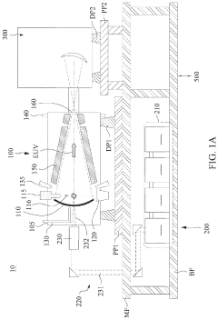
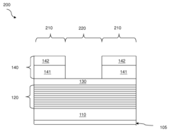
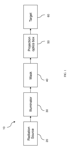
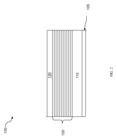
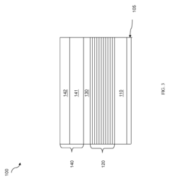
EUV lithography systems comprise specialized components designed to work with extreme ultraviolet light. These include EUV light sources, reflective optics (as opposed to refractive optics used in conventional lithography), specialized masks, and precision positioning systems. The systems operate in vacuum environments due to the high absorption of EUV light in air. These components work together to enable nanometer-scale pattern transfer for advanced semiconductor manufacturing.- EUV Lithography System Components: Extreme Ultraviolet (EUV) lithography systems comprise specialized components designed to work with short-wavelength light. These systems include EUV light sources, reflective optics (as traditional transmissive optics absorb EUV radiation), specialized masks, and precision positioning stages. The integration of these components enables the creation of semiconductor devices with feature sizes below 10nm, representing a significant advancement in lithography technology.
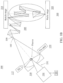
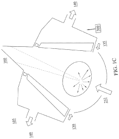
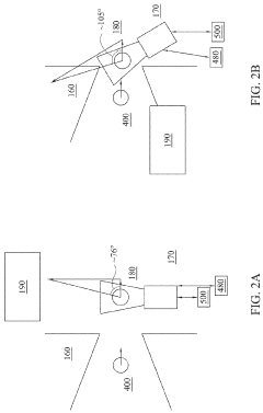
- EUV Source Technology: EUV lithography requires specialized light sources that can generate extreme ultraviolet radiation at approximately 13.5nm wavelength. These sources typically use laser-produced plasma or discharge-produced plasma technologies where high-energy lasers or electrical discharges strike targets (often tin droplets) to create EUV radiation. Innovations in this area focus on increasing source power, stability, and reliability while reducing debris generation that can contaminate optical components.
- Mask and Reticle Technology for EUV: EUV lithography employs reflective masks rather than the transmissive masks used in conventional lithography. These masks consist of multilayer reflective coatings with absorber patterns on top. Key innovations include defect mitigation strategies, pattern accuracy improvements, and methods to handle mask-induced imaging errors. Advanced inspection and repair technologies are critical for ensuring mask quality, as defects at this scale can significantly impact the final semiconductor device performance.
- EUV Optical Systems and Alignment: EUV optical systems use complex arrangements of multilayer mirrors to reflect and focus the EUV radiation. These systems require extreme precision in alignment and positioning, with tolerances in the sub-nanometer range. Innovations include advanced metrology systems for real-time monitoring, adaptive optics to correct for thermal and mechanical distortions, and sophisticated control algorithms to maintain optimal focus and alignment during exposure processes.
- Computational and Process Integration for EUV: EUV lithography requires sophisticated computational methods to optimize the lithographic process. This includes optical proximity correction, source mask optimization, and process window enhancement techniques. Additionally, integration with other semiconductor manufacturing steps is critical, including resist chemistry optimization, post-exposure processing, and metrology. Advanced modeling and simulation tools help predict and mitigate issues related to stochastic effects that become prominent at EUV wavelengths.
02 EUV Light Source Technology
EUV lithography requires specialized light sources that can generate extreme ultraviolet radiation at 13.5nm wavelength. These sources typically use laser-produced plasma or discharge-produced plasma technologies where high-energy lasers or electrical discharges strike tin droplets to create EUV photons. The light source systems include sophisticated debris mitigation, collector optics, and dose control mechanisms to ensure stable and reliable EUV output for the lithography process.Expand Specific Solutions03 Mask and Reticle Technology for EUV
EUV lithography uses reflective masks rather than the transmissive masks used in conventional lithography. These masks consist of multilayer reflective coatings with patterned absorber layers. The technology includes advanced methods for defect inspection, repair, and handling of EUV masks. Innovations in this area focus on improving mask lifetime, reducing defects, and enhancing pattern fidelity for increasingly smaller feature sizes.Expand Specific Solutions04 Thermal Management in EUV Systems
Thermal management is critical in EUV lithography systems due to the high power densities and heat loads generated during operation. Advanced cooling systems, temperature control mechanisms, and thermal expansion compensation techniques are employed to maintain dimensional stability and optical performance. These thermal management solutions address challenges in both the EUV source and the optical path to ensure consistent lithographic performance.Expand Specific Solutions05 Computational and Control Methods for EUV
Advanced computational and control methods are essential for EUV lithography performance. These include sophisticated algorithms for optical proximity correction, source mask optimization, and process window enhancement. Real-time control systems manage the complex interactions between subsystems, while computational lithography techniques compensate for physical limitations of EUV imaging. Machine learning approaches are increasingly applied to optimize process parameters and improve yield in EUV lithography.Expand Specific Solutions
Key EUV Equipment Manufacturers and Ecosystem
EUV Lithography is currently in the growth phase, with the global market expected to reach $10 billion by 2025. The technology has matured significantly but remains concentrated among few players. ASML Holding NV dominates the EUV equipment market as the sole supplier of production-ready EUV lithography systems, while companies like Carl Zeiss SMT provide critical optical components. Leading semiconductor manufacturers Taiwan Semiconductor Manufacturing Co., Samsung Electronics, and Intel are primary adopters, investing billions in EUV implementation. The supply chain complexity creates significant logistics challenges, with specialized materials from companies like Tokyo Electron and Applied Materials requiring precise coordination. This concentrated ecosystem makes the supply chain vulnerable to disruptions, necessitating strategic inventory management and alternative sourcing strategies.
Taiwan Semiconductor Manufacturing Co., Ltd.
Technical Solution: TSMC has pioneered the integration of EUV lithography into high-volume semiconductor manufacturing, beginning with their 7nm+ process and expanding to 5nm and 3nm nodes. The company has developed specialized supply chain protocols for EUV implementation, including dedicated clean room facilities with precise environmental controls and specialized transportation systems for EUV-related materials. TSMC maintains a multi-tiered supplier qualification system with rigorous certification processes for EUV-related materials and components, ensuring consistent quality across their global manufacturing network. Their logistics approach includes regional supplier clusters near major fabs to minimize transportation risks and reduce lead times for critical EUV materials. TSMC has implemented AI-driven predictive maintenance systems for EUV equipment, reducing unplanned downtime by approximately 30% and optimizing spare parts inventory. The company operates dedicated training facilities for EUV technicians and engineers, addressing the specialized workforce requirements of this advanced technology.
Strengths: Industry-leading implementation of EUV in high-volume manufacturing; sophisticated supplier qualification system; advanced predictive maintenance capabilities for EUV equipment. Weaknesses: High concentration of advanced manufacturing in geographically vulnerable Taiwan; extreme dependence on ASML as sole EUV equipment supplier; significant capital requirements for continued EUV expansion.
Carl Zeiss SMT GmbH
Technical Solution: Zeiss SMT is the exclusive supplier of the critical optical systems for ASML's EUV lithography machines, developing and manufacturing the complex optical components that enable EUV technology. Their EUV optical systems incorporate precision-engineered mirrors with surface accuracy to within 0.1nm, requiring specialized manufacturing and handling processes throughout the supply chain. Zeiss has developed proprietary coating technologies for EUV mirrors that achieve over 70% reflectivity at 13.5nm wavelength, essential for system performance. The company maintains dedicated clean room facilities with environmental controls exceeding ISO Class 1 standards, with particulate levels below 1 particle per cubic foot at 0.05μm. Their logistics system includes custom vibration-isolated transportation containers with continuous environmental monitoring for optical components. Zeiss has implemented a specialized supplier qualification program for EUV optical materials, with rigorous testing protocols for material purity and consistency. The company maintains strategic inventory of long-lead-time materials and components to mitigate supply chain disruptions.
Strengths: Unmatched expertise in EUV optics; close strategic partnership with ASML; proprietary manufacturing processes for critical optical components. Weaknesses: Single-source dependency for ASML's EUV systems creates supply chain vulnerability; extreme manufacturing complexity limits production scaling; specialized transportation requirements add logistics complexity and cost.
Critical Patents and Innovations in EUV Technology
Method and apparatus for mitigating contamination
PatentActiveUS20230273525A1
Innovation
- A supersonic gas jet with high-density hydrogen gas is employed at the intermediate focus to deflect tin nanoparticles away from the reticle, either alone or in combination with a low-level electromagnetic field, ensuring they do not contaminate the scanner side.
Extreme ultraviolet lithography process and mask
PatentActiveUS9448491B2
Innovation
- A mask structure incorporating a reflective multilayer with a flare-suppressing absorption stack (FSAS) and a flare-suppressing-by-phase-shifting (FSbPhS) layer, which absorbs EUV light and induces destructive interference to suppress OOB radiation, specifically DUV flare, enhancing image contrast and lithography performance.
Supply Chain Vulnerabilities and Resilience Strategies
The global EUV lithography supply chain exhibits significant vulnerabilities due to its highly concentrated nature. ASML's monopoly on EUV lithography systems creates a single point of failure that could disrupt the entire semiconductor manufacturing ecosystem. This concentration risk is compounded by the geographic clustering of critical suppliers, with key components sourced from specialized vendors in Europe, Japan, and the United States. Any disruption affecting these regions—whether from natural disasters, geopolitical tensions, or public health crises—can severely impact the availability of EUV systems.
Raw material dependencies present another layer of vulnerability. EUV lithography relies on rare earth elements and specialized materials with limited sourcing options. The mirrors essential for EUV systems require ultra-pure silicon and precise coatings that come from a handful of qualified suppliers. Similarly, the specialized photoresists and masks necessary for the process have few alternative sources, creating bottlenecks in the supply chain.
Geopolitical tensions have emerged as a significant threat to EUV supply chain stability. Export controls and technology restrictions between major economies have already affected the deployment of advanced lithography systems to certain markets. These restrictions not only impact immediate equipment availability but also influence long-term capacity planning and technology development trajectories across the semiconductor industry.
To address these vulnerabilities, semiconductor manufacturers are implementing multi-faceted resilience strategies. Inventory management has evolved beyond just-in-time approaches to include strategic stockpiling of critical components and materials. Leading chip manufacturers maintain safety stocks of essential EUV consumables and spare parts to mitigate short-term supply disruptions.
Supplier diversification efforts are underway, though limited by the specialized nature of EUV technology. Companies are investing in developing alternative sources for components where technically feasible, while establishing deeper collaborative relationships with existing suppliers to ensure preferential access during shortages.
Regional manufacturing strategies are being reconsidered, with major semiconductor players establishing more geographically distributed production capabilities. Government initiatives in the US, Europe, and Asia are supporting domestic semiconductor manufacturing capacity, including investments in the supporting ecosystem needed for advanced lithography.
Long-term resilience strategies include significant R&D investments in alternative lithography technologies that could eventually reduce dependence on EUV systems. Additionally, industry consortia are forming to address supply chain vulnerabilities collectively, sharing best practices and potentially coordinating procurement strategies to ensure more stable access to critical EUV components and systems.
Geopolitical Factors Affecting EUV Technology Access
The geopolitical landscape surrounding EUV lithography technology has become increasingly complex, with national security concerns and technological sovereignty emerging as critical factors influencing access to this advanced semiconductor manufacturing capability. The United States, in particular, has implemented export controls targeting China's access to EUV systems, citing dual-use concerns and potential military applications. These restrictions have been formalized through the Bureau of Industry and Security's Entity List and the Foreign Direct Product Rule, creating significant barriers for Chinese semiconductor manufacturers.
The Netherlands, home to ASML—the sole producer of commercial EUV lithography systems—has aligned with US policies, restricting exports of EUV technology to China. This alignment reflects broader geopolitical tensions and the formation of technology alliances aimed at maintaining Western technological advantages in critical sectors. The Dutch government's decision demonstrates how semiconductor technology has become a focal point in great power competition.
Japan and South Korea, both significant players in the semiconductor supply chain, have also faced pressure to restrict technology transfers to China. Their positions are complicated by economic dependencies on the Chinese market and their roles as suppliers of critical components for EUV systems. This tension illustrates the difficult balance between economic interests and security considerations that characterizes the current geopolitical environment.
The European Union has developed its European Chips Act partly in response to these geopolitical pressures, aiming to reduce dependency on external suppliers and secure access to critical technologies. Similarly, the CHIPS and Science Act in the United States provides substantial funding to rebuild domestic semiconductor manufacturing capabilities, reflecting concerns about supply chain vulnerabilities exposed during recent global disruptions.
Taiwan's position is particularly precarious, as it hosts TSMC, the world's leading contract chipmaker and a major user of EUV technology. Cross-strait tensions with China create significant geopolitical risks for global access to advanced semiconductor manufacturing capabilities, with potential implications for technology companies worldwide.
These geopolitical factors have accelerated efforts to develop indigenous alternatives to EUV lithography in countries facing access restrictions. China has increased investments in semiconductor self-sufficiency, though developing competitive alternatives to ASML's EUV technology remains a significant challenge due to the complex ecosystem of suppliers and intellectual property required.
The fragmentation of the global semiconductor supply chain along geopolitical lines threatens to increase costs, reduce efficiency, and potentially slow innovation in the sector. Companies must now navigate an increasingly complex landscape of regulations, alliances, and restrictions that directly impact their ability to access cutting-edge lithography technology.
Unlock deeper insights with Patsnap Eureka Quick Research — get a full tech report to explore trends and direct your research. Try now!
Generate Your Research Report Instantly with AI Agent
Supercharge your innovation with Patsnap Eureka AI Agent Platform!