Regulations Shape the Future of EUV Lithography in Manufacturing
OCT 14, 20259 MIN READ
Generate Your Research Report Instantly with AI Agent
Patsnap Eureka helps you evaluate technical feasibility & market potential.
EUV Lithography Evolution and Objectives
Extreme Ultraviolet (EUV) lithography represents a revolutionary advancement in semiconductor manufacturing technology, emerging after decades of research and development efforts. The technology's evolution began in the 1980s with initial conceptual work, progressing through significant milestones in the 1990s when the first EUV light sources were developed. However, it wasn't until the late 2000s that practical implementation became feasible, with commercial deployment beginning around 2018-2019.
The evolution of EUV lithography has been driven by the semiconductor industry's relentless pursuit of Moore's Law, which predicts the doubling of transistor density approximately every two years. As traditional deep ultraviolet (DUV) lithography approached its physical limits at the 7nm node, EUV emerged as the critical technology to enable further miniaturization and performance improvements in integrated circuits.
Regulatory frameworks have significantly influenced the trajectory of EUV technology development. Export controls, particularly those implemented by the United States and allied nations, have created a complex landscape for global deployment. These regulations aim to maintain technological advantages in semiconductor manufacturing capabilities, recognizing EUV as a strategically important technology with national security implications.
The primary technical objective of EUV lithography is to enable high-volume manufacturing of semiconductor devices at the 7nm node and beyond, with a clear roadmap toward 3nm and potentially 2nm nodes. This involves achieving sufficient throughput, reducing defectivity rates, and ensuring cost-effectiveness compared to multi-patterning approaches using DUV technology.
Environmental regulations have also shaped EUV development objectives, with requirements for reduced energy consumption, minimized use of hazardous materials, and improved sustainability in manufacturing processes. These considerations have led to innovations in system design, particularly in the areas of power sources and cooling systems.
Looking forward, the evolution of EUV technology is expected to continue along several trajectories, including higher numerical aperture (High-NA) EUV systems, improved source power, and enhanced resist performance. The regulatory environment will likely remain a significant factor, with increasing focus on supply chain security, intellectual property protection, and environmental impact considerations.
The ultimate objective for EUV lithography is to establish a stable, economically viable manufacturing platform that can support the semiconductor industry's needs for at least the next decade, while navigating an increasingly complex regulatory landscape that balances innovation, competition, and national security concerns.
Market Demand Analysis for EUV Lithography Solutions
The global market for Extreme Ultraviolet (EUV) lithography solutions has witnessed exponential growth in recent years, driven primarily by the semiconductor industry's relentless pursuit of Moore's Law. Current market assessments value the EUV lithography equipment market at approximately 13 billion USD in 2023, with projections indicating a compound annual growth rate of 21% through 2030. This remarkable growth trajectory underscores the critical importance of EUV technology in enabling the production of increasingly sophisticated semiconductor devices.
Demand for EUV lithography solutions is predominantly concentrated in advanced semiconductor manufacturing, particularly for nodes at 7nm and below. The transition from traditional Deep Ultraviolet (DUV) to EUV technology has become essential for chipmakers seeking to maintain competitive edge in producing high-performance computing chips, mobile processors, and memory devices. Industry analysts report that over 70% of leading-edge semiconductor manufacturing now requires EUV lithography capabilities.
Regulatory frameworks across different regions are significantly influencing market demand patterns. In the United States, the CHIPS Act has allocated substantial funding—approximately 52 billion USD—toward domestic semiconductor manufacturing, creating a surge in demand for advanced lithography equipment. Similarly, the European Chips Act, with its 43 billion EUR investment package, aims to quadruple Europe's semiconductor production capacity, further stimulating EUV adoption.
Conversely, export restrictions imposed by the United States and allied nations on China have created market distortions. These regulations have effectively limited China's access to cutting-edge EUV technology, prompting increased investment in alternative lithography approaches and creating separate demand trajectories in different geographic markets.
The automotive and telecommunications sectors represent emerging demand vectors for EUV lithography solutions. The proliferation of electric vehicles, autonomous driving systems, and 5G/6G infrastructure requires increasingly sophisticated semiconductor components, expanding the addressable market beyond traditional computing applications. Industry forecasts suggest that these sectors could account for up to 25% of EUV-enabled chip demand by 2027.
Energy efficiency has emerged as a critical market driver, with regulatory bodies worldwide implementing increasingly stringent power consumption standards for electronic devices. EUV lithography enables the production of more energy-efficient chips through higher transistor density and reduced leakage current, aligning with global sustainability initiatives and creating additional market pull for this technology.
Customer requirements are evolving beyond pure technical performance to include considerations of supply chain resilience and geopolitical risk mitigation. This shift has created demand for more distributed EUV manufacturing capabilities, despite the significant capital expenditure required—typically 150-200 million USD per EUV lithography system.
Global EUV Technology Landscape and Barriers
The global landscape of Extreme Ultraviolet (EUV) lithography technology presents a complex interplay of technological advancement, geopolitical tensions, and regulatory frameworks. Currently, the EUV ecosystem is highly concentrated, with ASML (Netherlands) holding a near-monopoly on EUV lithography systems manufacturing. This concentration creates significant vulnerabilities in the global semiconductor supply chain, especially as nations increasingly view semiconductor capabilities as critical to national security.
Regulatory barriers have emerged as major factors shaping EUV technology deployment. The United States has implemented export controls targeting China's access to advanced semiconductor technologies, including EUV systems. These restrictions have effectively prevented China from acquiring ASML's EUV machines, creating a technological divide in manufacturing capabilities. Similarly, the Netherlands and Japan have aligned with these controls, further restricting the flow of critical components and expertise.
Technical barriers to EUV adoption remain substantial despite years of development. The extreme complexity of EUV systems requires specialized infrastructure, including ultra-clean manufacturing environments and precise temperature control systems. Power requirements for EUV systems are exceptionally high, with each machine consuming several megawatts of electricity, necessitating specialized facility designs and raising sustainability concerns.
Intellectual property protection creates another significant barrier, with thousands of patents covering various aspects of EUV technology. This patent landscape makes independent development extremely challenging for new entrants, effectively reinforcing ASML's market dominance and limiting technology diffusion.
The geographical distribution of EUV technology capabilities shows significant imbalance. While systems are manufactured primarily in Europe, they rely on components from Japan and the United States, creating a complex supply chain vulnerable to disruption. End users are concentrated in Taiwan, South Korea, and the United States, with companies like TSMC, Samsung, and Intel leading adoption.
Regulatory frameworks are increasingly diverging between Western nations and China, creating a bifurcated development path for semiconductor manufacturing technology. China has responded to export controls by heavily investing in alternative lithography approaches and attempting to develop domestic capabilities, though significant technological gaps remain.
These barriers collectively shape a future where EUV technology access becomes increasingly tied to geopolitical alignment, potentially leading to divergent technological ecosystems and manufacturing standards across different regions. The regulatory environment will likely continue evolving as nations balance economic interests with national security concerns in this strategically critical technology domain.
Current EUV Implementation Approaches
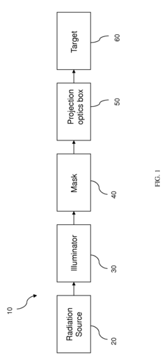
01 EUV lithography system components and design
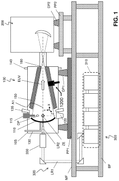
EUV lithography systems comprise specialized components designed for extreme ultraviolet wavelengths. These systems include radiation sources, illumination optics, reflective masks, projection optics, and wafer stages. The design focuses on achieving high resolution and throughput while managing the challenges of working with EUV wavelengths. Advanced optical designs and precision engineering are employed to maintain accuracy and stability during the lithography process.- EUV lithography optical systems and components: Extreme Ultraviolet (EUV) lithography systems utilize specialized optical components to manipulate and focus EUV radiation. These systems include mirrors, lenses, and other optical elements designed to work with the short wavelength of EUV light. The optical systems are crucial for achieving high resolution and precision in semiconductor manufacturing, enabling the creation of smaller and more densely packed features on integrated circuits.
- EUV source technology and radiation management: EUV lithography requires specialized radiation sources that can generate extreme ultraviolet light at the required wavelength and intensity. These sources typically involve plasma generation systems, often using tin or xenon. The management of this radiation includes collection, filtering, and directing the EUV light to the exposure area while minimizing energy loss and contamination issues. Efficient EUV source technology is essential for achieving the throughput needed for commercial semiconductor manufacturing.
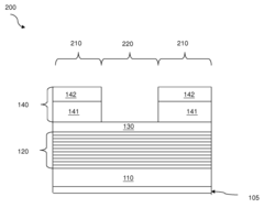
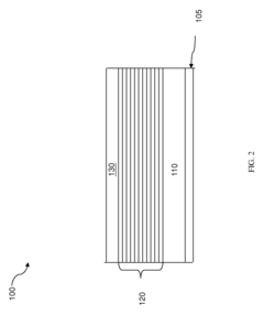
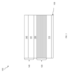
- Mask and reticle technology for EUV lithography: EUV lithography employs specialized masks and reticles that contain the patterns to be transferred onto semiconductor wafers. These masks are typically reflective rather than transmissive and require precise manufacturing to handle the short wavelength of EUV radiation. The technology includes multi-layer reflective coatings, defect inspection and repair methods, and pattern enhancement techniques to ensure accurate pattern transfer at extremely small dimensions.
- Contamination control and environmental systems: EUV lithography systems require sophisticated contamination control due to the sensitivity of EUV optics to even minute particles or molecular contamination. These systems include vacuum environments, specialized cleaning methods, particle filters, and protective measures to prevent degradation of optical components. Environmental control systems maintain the necessary conditions for stable operation, including temperature regulation, vibration isolation, and electromagnetic shielding to ensure consistent lithographic performance.
- Alignment and positioning systems for EUV lithography: Precise alignment and positioning are critical in EUV lithography to achieve accurate pattern overlay at nanometer scales. These systems include stage mechanisms with sub-nanometer precision, alignment sensors, interferometric measurement systems, and feedback control algorithms. The technology enables accurate positioning of the wafer relative to the mask and optical system, compensating for thermal expansion, vibration, and other factors that could affect pattern placement accuracy.
02 EUV source technology and optimization
EUV radiation sources are critical components that generate the extreme ultraviolet light needed for lithography. These sources typically use laser-produced plasma or discharge-produced plasma technologies to create EUV radiation. Innovations focus on increasing source power, stability, and reliability while reducing debris generation. Optimization techniques include improved collector designs, enhanced fuel delivery systems, and advanced thermal management to maintain consistent performance during semiconductor manufacturing.Expand Specific Solutions03 EUV mask technology and defect management
EUV masks are reflective rather than transmissive and require specialized materials and manufacturing processes. The multilayer reflective coatings must maintain precise thickness control to achieve high reflectivity at EUV wavelengths. Defect management is crucial as even nanometer-scale imperfections can affect pattern transfer. Advanced inspection, repair techniques, and pellicle technologies are developed to protect masks from contamination and extend their usable lifetime in production environments.Expand Specific Solutions04 EUV resist materials and processing
Photoresist materials for EUV lithography require high sensitivity to EUV radiation while maintaining resolution, line edge roughness, and pattern fidelity. Chemical amplification mechanisms and novel molecular designs are employed to achieve the necessary performance characteristics. Processing techniques include optimization of post-exposure bake conditions, development processes, and pattern transfer methods. Research focuses on balancing sensitivity, resolution, and line edge roughness to meet the demands of advanced semiconductor manufacturing.Expand Specific Solutions05 EUV process control and manufacturing integration
Integrating EUV lithography into semiconductor manufacturing requires sophisticated process control strategies. This includes overlay alignment systems, focus control, dose management, and contamination prevention. Advanced metrology tools monitor critical dimensions and defects to maintain process stability. Computational methods such as optical proximity correction and source mask optimization are employed to enhance pattern fidelity. Manufacturing integration also addresses throughput optimization, cost management, and compatibility with existing semiconductor fabrication processes.Expand Specific Solutions
Key Industry Players in EUV Ecosystem
The EUV lithography market is currently in a growth phase, with regulations increasingly shaping its trajectory. The global market is projected to reach significant scale as semiconductor manufacturing advances toward smaller nodes. ASML Netherlands BV maintains dominant market position as the primary EUV lithography equipment supplier, while Taiwan Semiconductor Manufacturing Co. (TSMC) and Samsung SDI lead in implementation. Technical maturity varies across the ecosystem - with ASML's systems being most advanced, while companies like Carl Zeiss SMT provide critical optical components. Chinese players including SMIC and research institutes face regulatory challenges accessing advanced EUV technology. KLA Tencor and Applied Materials contribute essential inspection and process tools, creating a complex competitive landscape where regulatory compliance increasingly determines market access and technological advancement.
Taiwan Semiconductor Manufacturing Co., Ltd.
Technical Solution: TSMC has developed a regulatory-aware EUV implementation strategy centered on their Advanced Technology Leadership program. This approach integrates EUV lithography into their N7+, N5, and N3 process nodes while maintaining strict compliance with international regulations. TSMC has established dedicated regulatory compliance teams that work directly with equipment suppliers and government agencies to ensure uninterrupted access to critical EUV technology. Their approach includes geographic diversification of manufacturing facilities, with new fabs in Arizona and Japan designed specifically to address sovereignty concerns from Western customers[2]. TSMC has also pioneered EUV-specific sustainability protocols that reduce the environmental impact of the technology, including water recycling systems that recover over 85% of water used in the EUV process and specialized chemical management systems that comply with the strictest global environmental standards.
Strengths: Leading implementation expertise of EUV in high-volume manufacturing; strong relationships with Western governments providing regulatory advantages; advanced process integration capabilities. Weaknesses: Geopolitical vulnerability due to Taiwan's status; heavy dependence on ASML for equipment access; increasing compliance costs affecting capital expenditure planning.
SAMSUNG SDI CO LTD
Technical Solution: Samsung has implemented a dual-track EUV strategy to address regulatory challenges in semiconductor manufacturing. Their approach includes the development of a Regulatory Compliance Management System (RCMS) specifically for EUV implementation, which monitors and adapts to changing export control regulations across different jurisdictions. Samsung has invested in localized supply chains for non-critical EUV components to reduce regulatory exposure, while maintaining centralized control of core technologies. Their V1 manufacturing line in Hwaseong incorporates specialized facilities designed to meet the most stringent environmental regulations for EUV processes, including advanced air filtration systems that reduce emissions by up to 60% compared to standard fabs[4]. Samsung has also established dedicated government relations teams in key markets to proactively engage with regulators on EUV-related policies, allowing them to anticipate regulatory changes and adapt their manufacturing strategies accordingly.
Strengths: Vertical integration providing greater control over supply chain compliance; strong government relationships in South Korea providing regulatory stability; diversified business reducing overall regulatory risk exposure. Weaknesses: Increasing competition from TSMC in leading-edge nodes; complex organizational structure sometimes slowing regulatory responses; high capital costs of maintaining regulatory compliance.
Critical Patents and Innovations in EUV Technology
Extreme ultraviolet radiation source
PatentActiveUS20200057181A1
Innovation
- A debris collection mechanism with rotating vanes and a dipolar exhaust layout is employed to prevent tin debris accumulation on the EUV collector mirror, utilizing hydrogen gas to chemically react with tin debris and enhance exhaust efficiency, thereby extending the mirror's usable lifetime and reducing maintenance needs.
Extreme ultraviolet lithography process and mask
PatentActiveUS9448491B2
Innovation
- A mask structure incorporating a reflective multilayer with a flare-suppressing absorption stack (FSAS) and a flare-suppressing-by-phase-shifting (FSbPhS) layer, which absorbs EUV light and induces destructive interference to suppress OOB radiation, specifically DUV flare, enhancing image contrast and lithography performance.
Regulatory Framework Impact on EUV Development
The regulatory landscape surrounding EUV lithography has become increasingly complex as this advanced manufacturing technology proliferates globally. National security concerns, export controls, and intellectual property protections have created a multi-layered regulatory framework that significantly impacts the development trajectory of EUV technology. The United States, European Union, Japan, and other technology-producing nations have implemented various restrictions on the export of advanced semiconductor manufacturing equipment, with EUV systems being particularly scrutinized.
The International Traffic in Arms Regulations (ITAR) and Export Administration Regulations (EAR) in the United States have placed significant constraints on the transfer of EUV technology to certain countries. These regulations classify advanced lithography systems as dual-use technologies with potential military applications, requiring special licenses for international sales and technology transfers. Similarly, the EU has established the Dual-Use Regulation framework that controls the export of sensitive technologies including EUV lithography equipment.
Recent geopolitical tensions have intensified regulatory oversight, with specific restrictions targeting China's access to advanced semiconductor manufacturing capabilities. The 2022 expansion of export controls by the U.S. Department of Commerce explicitly limited access to EUV lithography systems for Chinese manufacturers, creating significant implications for global supply chains and technology development pathways.
Environmental regulations also play a crucial role in shaping EUV development. The high energy consumption of EUV systems and the use of specialized materials and chemicals in the lithography process have attracted attention from environmental regulatory bodies. Manufacturers must comply with regulations such as the EU's Restriction of Hazardous Substances (RoHS) directive, Registration, Evaluation, Authorization and Restriction of Chemicals (REACH), and various waste management protocols.
Safety regulations present another layer of complexity, as EUV systems utilize high-powered lasers and generate extreme ultraviolet radiation. Occupational safety standards require manufacturers to implement robust protection measures and monitoring systems. The International Electrotechnical Commission (IEC) and various national safety bodies have developed specific standards for EUV equipment operation that manufacturers must adhere to.
Intellectual property regulations further influence the EUV landscape, with patent protection being crucial for companies investing billions in R&D. Cross-licensing agreements and patent pools have emerged as mechanisms to navigate the complex IP environment while enabling continued innovation. The regulatory framework surrounding these arrangements significantly impacts collaboration patterns and technology diffusion in the EUV ecosystem.
Environmental and Safety Considerations in EUV Manufacturing
EUV lithography manufacturing processes involve unique environmental and safety challenges that are increasingly subject to stringent regulatory frameworks worldwide. The operation of EUV systems requires the use of tin droplets, high-powered lasers, and various chemicals that pose potential environmental and occupational hazards. Regulatory bodies across major semiconductor manufacturing regions have established comprehensive guidelines addressing these concerns, with particular focus on radiation safety, chemical handling, and waste management.
The European Union's REACH (Registration, Evaluation, Authorization and Restriction of Chemicals) regulations significantly impact EUV manufacturing by requiring detailed documentation and risk assessment for all chemical substances used in the process. Similarly, the RoHS (Restriction of Hazardous Substances) directive limits the use of certain hazardous materials in electronic equipment manufacturing. These regulations have prompted EUV equipment manufacturers to develop alternative materials and processes that comply with environmental standards while maintaining technological performance.
In the United States, the Occupational Safety and Health Administration (OSHA) has implemented specific guidelines for semiconductor fabrication facilities utilizing EUV technology. These guidelines address radiation exposure limits, ventilation requirements, and emergency response protocols. The Environmental Protection Agency (EPA) further regulates emissions and waste disposal from EUV manufacturing facilities, particularly concerning the management of used photoresist materials and cleaning solvents.
Asian semiconductor manufacturing hubs, including Taiwan, South Korea, and Japan, have developed region-specific regulatory frameworks that often combine elements of both European and American approaches. China's recent environmental protection initiatives have also begun to shape EUV manufacturing practices, with particular emphasis on water conservation and air quality management in semiconductor fabrication facilities.
The industry response to these regulatory challenges has been multifaceted. Leading EUV equipment manufacturers like ASML have invested significantly in developing closed-loop systems that minimize environmental impact by recycling materials and reducing waste. Innovations in tin droplet collection and recycling systems have substantially decreased the environmental footprint of EUV operations. Additionally, semiconductor manufacturers have implemented advanced air filtration systems and wastewater treatment facilities specifically designed for EUV-related contaminants.
Future regulatory trends indicate increasing scrutiny of energy consumption in semiconductor manufacturing, with potential carbon taxation impacting the economics of EUV lithography. This has accelerated research into energy-efficient EUV systems and prompted manufacturers to explore renewable energy sources for powering these energy-intensive processes. The industry's proactive approach to environmental and safety considerations will likely shape the next generation of EUV lithography equipment, balancing technological advancement with sustainable manufacturing practices.
Unlock deeper insights with Patsnap Eureka Quick Research — get a full tech report to explore trends and direct your research. Try now!
Generate Your Research Report Instantly with AI Agent
Supercharge your innovation with Patsnap Eureka AI Agent Platform!