What Drives the Adoption of EUV Lithography in Complex IC Designs
OCT 14, 20259 MIN READ
Generate Your Research Report Instantly with AI Agent
Patsnap Eureka helps you evaluate technical feasibility & market potential.
EUV Lithography Evolution and Objectives
Extreme Ultraviolet (EUV) lithography represents a revolutionary advancement in semiconductor manufacturing technology, marking a significant departure from traditional Deep Ultraviolet (DUV) lithography methods. The evolution of EUV technology spans over three decades, beginning in the 1980s with initial research into short-wavelength lithography techniques. By the 1990s, EUV emerged as a promising candidate for next-generation lithography, though significant technical challenges remained unresolved.
The development trajectory accelerated in the early 2000s when industry consortia like ASML, Intel, and Samsung intensified their collaborative efforts to overcome the fundamental barriers to EUV implementation. These challenges included developing reliable high-power light sources, creating effective reflective optics, and designing specialized photoresist materials capable of responding to 13.5nm wavelength light.
A critical milestone occurred in 2016-2017 when ASML delivered the first commercial EUV lithography systems capable of high-volume manufacturing. This breakthrough enabled the industry to progress beyond the limitations of multi-patterning techniques that had become increasingly complex and costly at advanced nodes. The subsequent years witnessed rapid improvements in EUV system throughput, reliability, and resolution capabilities.
The primary objective driving EUV adoption is the continuation of Moore's Law in an era where traditional scaling approaches face diminishing returns. EUV lithography, with its 13.5nm wavelength (compared to 193nm for DUV), enables the printing of significantly smaller features in a single exposure step, dramatically reducing the complexity of advanced node manufacturing processes.
Additional objectives include cost reduction through process simplification, as EUV can replace multiple DUV exposures with a single step. This translates to fewer masks, reduced process variability, and improved yields for complex designs. Furthermore, EUV technology aims to enable new device architectures that were previously impractical due to alignment challenges in multi-patterning approaches.
Looking forward, the industry has established a clear roadmap for EUV technology evolution, including high-NA (numerical aperture) EUV systems currently under development. These next-generation tools promise to extend EUV lithography's capabilities to even smaller feature sizes, potentially enabling semiconductor scaling well into the sub-3nm node era. The ultimate goal remains enabling continued innovation in integrated circuit design and performance while managing manufacturing complexity and cost.
Semiconductor Market Demand Analysis
The semiconductor industry is experiencing unprecedented demand for advanced integrated circuits (ICs) driven by emerging technologies such as artificial intelligence, 5G networks, autonomous vehicles, and high-performance computing. This market evolution has created significant pressure for more powerful, energy-efficient, and compact semiconductor devices, directly influencing the adoption of Extreme Ultraviolet (EUV) lithography technology.
Market research indicates that the global semiconductor market is projected to reach $1 trillion by 2030, with advanced nodes (7nm and below) representing the fastest-growing segment. These advanced nodes, which benefit most from EUV lithography, are expected to grow at a compound annual growth rate of 19% through 2026, significantly outpacing the broader semiconductor market growth of 7-8%.
The demand for complex IC designs is particularly strong in data centers and AI applications, where computational requirements are doubling approximately every 3-4 months. This acceleration has created a technology pull for EUV lithography, as traditional deep ultraviolet (DUV) lithography reaches its physical limits in achieving the required feature sizes and densities.
Mobile device manufacturers represent another significant market driver, with premium smartphones incorporating increasingly sophisticated chips manufactured at 5nm and below. The transition to 5G has further accelerated this trend, with RF components and baseband processors requiring higher integration densities achievable primarily through EUV processes.
Automotive semiconductor demand is also evolving rapidly, with advanced driver-assistance systems (ADAS) and electric vehicle control systems requiring more sophisticated ICs. Industry forecasts suggest automotive semiconductor content will increase from approximately $500 per vehicle in 2021 to over $1,000 by 2030, with a growing percentage requiring advanced node manufacturing.
Geographically, East Asia dominates semiconductor demand, accounting for over 60% of global consumption, followed by North America at approximately 24%. This regional concentration influences EUV adoption strategies, as manufacturers align capacity investments with market proximity.
The economic implications of EUV adoption are substantial, with cost-per-wafer considerations balanced against performance gains. While EUV lithography increases manufacturing costs by 15-20% compared to multiple-patterning DUV approaches, it enables approximately 30% higher transistor density and reduces overall process complexity, creating compelling economics for high-value applications.
Customer willingness to pay premium prices for advanced node chips manufactured using EUV technology has been validated across multiple market segments, particularly in high-performance computing, premium mobile devices, and AI accelerators, where performance advantages translate directly to competitive differentiation and market share gains.
EUV Technology Status and Barriers
Extreme Ultraviolet (EUV) lithography represents a significant technological breakthrough in semiconductor manufacturing, currently deployed primarily in advanced nodes below 7nm. The global landscape of EUV technology shows concentration in specific regions, with the Netherlands, Japan, and the United States leading research and implementation efforts, while South Korea, Taiwan, and China are rapidly advancing their capabilities.
Despite its revolutionary potential, EUV lithography faces several critical technical barriers. Power source stability remains a fundamental challenge, as current EUV light sources struggle to maintain consistent high power levels needed for volume production. The 13.5nm wavelength light requires approximately 250W of source power for economically viable throughput, but achieving this consistently while maintaining uptime above 80% continues to challenge manufacturers.
Mask infrastructure presents another significant hurdle. EUV masks are fundamentally different from traditional optical masks, requiring specialized blank materials, unique absorber stacks, and complex pellicle solutions. Defect-free mask production remains difficult, with defect inspection and repair technologies still evolving to meet the stringent requirements of sub-7nm nodes.
Photoresist performance constitutes a critical technical barrier. The high-energy photons in EUV exposure create different chemical reactions compared to traditional lithography, necessitating novel resist chemistries. Current EUV resists face a challenging trade-off between sensitivity, resolution, and line-edge roughness—the so-called "triangle of death" in resist development.
Pattern fidelity issues emerge as designs become more complex. Stochastic effects, where random variations in photon absorption and secondary electron generation lead to unpredictable pattern defects, become increasingly problematic at smaller feature sizes. These effects can cause missing contacts, bridge defects, and line breaks that significantly impact yield.
Integration challenges with existing semiconductor manufacturing processes represent another barrier. EUV lithography requires adjustments to surrounding processes, including etching, deposition, and metrology. The transition from multi-patterning approaches to EUV single patterning demands substantial process reengineering.
Economic barriers complement technical challenges. The extreme cost of EUV equipment—with each lithography tool exceeding $150 million—limits adoption to only the largest semiconductor manufacturers. Additionally, the specialized knowledge required for EUV operation creates workforce development challenges, as the industry faces a shortage of engineers and technicians with relevant expertise.
Current EUV Implementation Strategies
01 EUV lithography system design and optimization
EUV lithography systems require specialized design considerations to achieve optimal performance. These systems incorporate advanced optical components, precise alignment mechanisms, and sophisticated control systems to handle the unique challenges of extreme ultraviolet wavelengths. Innovations in system architecture focus on improving resolution, reducing defects, and enhancing throughput for semiconductor manufacturing applications.- EUV Lithography System Design and Components: EUV lithography systems require specialized components to handle extreme ultraviolet light. These systems include specialized mirrors, light sources, and optical arrangements that can effectively manipulate EUV radiation. The design must account for the unique properties of EUV light, including its absorption by most materials and the need for vacuum environments. Advanced optical systems and precise positioning mechanisms are essential for achieving the nanometer-scale resolution required for modern semiconductor manufacturing.
- EUV Mask Technology and Defect Management: EUV masks are critical components that require specialized manufacturing and inspection techniques. These masks use reflective rather than transmissive designs and must be free of defects at the nanometer scale. Technologies for detecting, characterizing, and repairing mask defects are essential for successful EUV lithography adoption. Advanced inspection tools and computational methods help identify potential issues before they affect production, while innovative mask designs help mitigate the impact of unavoidable defects.
- EUV Resist Materials and Processing: Specialized photoresist materials are required for EUV lithography that can respond effectively to the high-energy photons while maintaining resolution, sensitivity, and line edge roughness requirements. These materials must be optimized for the unique exposure mechanisms of EUV radiation. Processing techniques for these resists, including development, etching, and pattern transfer, must be adapted to work with the extremely small feature sizes enabled by EUV technology. Chemical amplification and novel molecular designs help achieve the necessary performance characteristics.
- EUV Integration with Manufacturing Processes: Integrating EUV lithography into existing semiconductor manufacturing workflows presents significant challenges. This includes developing compatible process steps before and after exposure, managing thermal effects, and ensuring proper alignment with previous layers. Factory automation systems must be adapted to handle the unique requirements of EUV tools, including specialized maintenance procedures and environmental controls. Computational methods for optimizing process parameters and predicting outcomes help maximize yield and performance in production environments.
- EUV Economic and Performance Considerations: The adoption of EUV lithography involves significant economic considerations, including high tool costs, throughput challenges, and power requirements. Manufacturers must balance these factors against the benefits of increased resolution and reduced multi-patterning steps. Performance metrics such as uptime, availability, and cost per wafer are critical for determining the economic viability of EUV adoption. Strategies for maximizing return on investment include optimizing tool utilization, extending consumable lifetimes, and developing more efficient operational procedures.
02 EUV source technology and development
The development of reliable and powerful EUV light sources is critical for the adoption of EUV lithography in semiconductor manufacturing. These sources typically utilize laser-produced plasma or discharge-produced plasma to generate extreme ultraviolet radiation. Innovations focus on increasing source power, stability, and lifetime while reducing operational costs and maintenance requirements to enable high-volume manufacturing.Expand Specific Solutions03 EUV mask and reticle technology
EUV lithography requires specialized reflective masks rather than traditional transmissive photomasks. These masks consist of multilayer reflective coatings with absorber patterns and must meet stringent requirements for defect control, pattern accuracy, and durability. Innovations in mask technology focus on improving reflectivity, reducing defects, enhancing pattern fidelity, and developing effective inspection and repair methods.Expand Specific Solutions04 EUV resist materials and processes
Specialized photoresist materials are essential for EUV lithography to achieve high resolution and sensitivity while minimizing line edge roughness. These materials must efficiently absorb EUV radiation and provide the chemical amplification necessary for pattern formation. Innovations focus on developing resist formulations with improved sensitivity, resolution, line edge roughness, and pattern collapse resistance to meet the demands of advanced semiconductor manufacturing.Expand Specific Solutions05 EUV integration and manufacturing challenges
The integration of EUV lithography into semiconductor manufacturing presents numerous challenges including contamination control, vacuum requirements, and compatibility with existing processes. Solutions involve developing specialized clean environments, vacuum systems, and process integration strategies. Innovations focus on overcoming these challenges to enable high-volume manufacturing with acceptable yields, throughput, and cost-effectiveness for advanced technology nodes.Expand Specific Solutions
Leading EUV Equipment Manufacturers and Chipmakers
EUV lithography adoption in complex IC designs is currently in a growth phase, with the market expected to expand significantly due to increasing demand for advanced semiconductor nodes. The technology has reached commercial maturity but continues to evolve rapidly. Taiwan Semiconductor Manufacturing Co. (TSMC) and Samsung Electronics lead implementation at 5nm and below nodes, while ASML Netherlands remains the dominant equipment supplier. GlobalFoundries and IBM are advancing integration capabilities for specialized applications. The ecosystem includes critical materials suppliers like AGC and SCHOTT AG supporting photomask and optical components. The competitive landscape shows a clear stratification between leading-edge manufacturers with EUV capabilities and those focusing on mature nodes, with significant barriers to entry due to the multi-billion dollar investments required.
Taiwan Semiconductor Manufacturing Co., Ltd.
Technical Solution: TSMC has pioneered the industrial implementation of EUV lithography, integrating it first in their 7nm+ process and extensively in their 5nm and 3nm nodes. Their EUV adoption strategy involves a multi-layered approach that combines process optimization, design rule modifications, and custom computational lithography techniques. TSMC's EUV implementation utilizes single-exposure patterning for critical layers, reducing multi-patterning steps and improving yield. Their process integrates specialized resists with sensitivity optimized for EUV wavelengths and custom pellicle solutions to enhance mask lifetime. TSMC has developed proprietary computational lithography algorithms that compensate for stochastic effects inherent to EUV, including dedicated solutions for edge placement error correction and source mask optimization. Their N3 (3nm) process technology employs EUV for over 20 critical layers, enabling transistor densities exceeding 250 million transistors per square millimeter while maintaining power efficiency improvements of 25-30% compared to previous nodes.
Strengths: Industry-leading implementation expertise with proven high-volume manufacturing capability; comprehensive design enablement ecosystem supporting customer adoption; demonstrated yield management expertise for EUV processes. Weaknesses: Extremely high capital expenditure requirements for EUV implementation; dependency on limited EUV equipment suppliers; challenges in managing increased cycle times for complex EUV layers.
Samsung Electronics Co., Ltd.
Technical Solution: Samsung has developed a comprehensive EUV implementation strategy across both memory and logic semiconductor production. Their V-NAND technology now incorporates EUV for critical patterning steps in advanced nodes, while their foundry business utilizes EUV extensively in 7nm and smaller processes. Samsung's approach includes specialized resist chemistry optimized for their specific device architectures, with sensitivity tuned to maximize throughput while maintaining pattern fidelity. Their EUV implementation includes proprietary computational lithography techniques that address specific challenges in memory cell patterning, where regular arrays benefit from customized source shape optimization. Samsung has pioneered the use of EUV for DRAM production, applying it to critical wordline and bitline formation in their DDR5 products. Their 3nm GAA (Gate-All-Around) process technology leverages EUV for multiple critical layers, enabling their multi-bridge channel FET (MBCFET) architecture that delivers improved electrostatic control and performance characteristics compared to conventional FinFET designs.
Strengths: Vertical integration allowing coordinated EUV implementation across diverse product lines; significant R&D resources enabling parallel development paths; ability to leverage learning across memory and logic applications. Weaknesses: Historically lower yields compared to TSMC in leading-edge nodes; challenges in EUV pellicle adoption affecting defect rates; complex coordination required between memory and foundry business units.
Critical EUV Patents and Technical Innovations
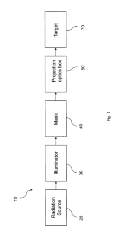
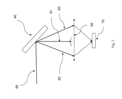
Extreme ultraviolet lithography process and mask
PatentActiveUS20160306272A1
Innovation
- The implementation of an EUV lithography system using a reflective mask with three states having specific reflection coefficients, combined with nearly on-axis illumination of partial coherence less than 0.3, and a projection optics box that removes most non-diffracted light to enhance pattern contrast and throughput.
System and Method for Extreme Ultraviolet Source Control
PatentActiveUS20210068241A1
Innovation
- The system employs a dual-pulse laser-produced plasma mechanism with optimized parameters, including pre-pulses and main pulses, to enhance EUV conversion efficiency and minimize debris deposition on the LPP collector by controlling the speed and geometry of target plumes, using a controller to adjust laser pulse energy and timing for optimal EUV radiation generation and collector protection.
Economic Impact of EUV Adoption
The adoption of Extreme Ultraviolet (EUV) lithography represents a significant economic inflection point in the semiconductor industry, with far-reaching implications across the global technology ecosystem. Initial capital expenditure for EUV implementation is substantial, with each lithography system costing upwards of $150 million, plus additional infrastructure investments ranging from $20-50 million for specialized clean rooms and supporting equipment. Despite these high entry costs, leading semiconductor manufacturers have committed billions to EUV adoption due to compelling long-term economic benefits.
Cost analysis reveals that while EUV systems require 2-3x higher initial investment than traditional immersion lithography, they deliver 30-40% reduction in process steps for advanced nodes, translating to significant operational savings. For 5nm processes and beyond, EUV adoption reduces mask counts by approximately 25-30%, decreasing manufacturing complexity and time-to-market for new chip designs.
The economic ripple effects extend throughout the semiconductor value chain. EUV enables continued node scaling, preserving Moore's Law economics with 15-20% cost reduction per transistor at advanced nodes compared to multi-patterning alternatives. This cost advantage becomes increasingly pronounced at 3nm and below, where traditional lithography approaches face diminishing returns and escalating costs.
For semiconductor equipment suppliers, EUV represents a market opportunity exceeding $10 billion annually by 2025. The specialized nature of EUV technology has reinforced ASML's market position, creating significant economic concentration in the equipment sector. Simultaneously, material suppliers have developed specialized EUV-specific offerings, creating new high-margin product categories.
From a macroeconomic perspective, EUV adoption enables continued advancement of computing capabilities that underpin artificial intelligence, 5G/6G communications, and other emerging technologies estimated to contribute $15-20 trillion to global GDP by 2030. Regions with EUV manufacturing capability gain strategic economic advantages in the increasingly critical semiconductor supply chain.
The return on investment timeline for EUV adoption typically spans 3-5 years, with profitability accelerating as production volumes increase and yields improve. Early adopters like TSMC and Samsung have reported that despite higher initial costs, EUV implementation has improved their competitive position and profit margins on premium nodes, allowing them to command price premiums of 15-25% for EUV-manufactured chips.
Supply Chain Resilience for EUV Technology
The global EUV lithography supply chain represents a complex ecosystem with significant vulnerabilities due to its concentrated nature. ASML, headquartered in the Netherlands, maintains a near-monopoly on EUV lithography systems, creating a critical dependency point for the entire semiconductor industry. This concentration of manufacturing capability presents substantial geopolitical and business continuity risks, particularly as international tensions rise around advanced semiconductor technologies.
Raw material sourcing for EUV systems presents another vulnerability layer. Critical components such as specialized mirrors require rare materials including ruthenium and specific isotopes of hydrogen. These materials often originate from limited geographical locations, creating potential bottlenecks during supply disruptions. The COVID-19 pandemic demonstrated how quickly these supply chains can be compromised, with delivery times for EUV systems extending significantly during 2020-2021.
Component manufacturing for EUV systems involves a network of specialized suppliers across multiple countries. Zeiss in Germany produces the crucial optical systems, while various precision components come from suppliers in Japan, the United States, and Europe. This distributed manufacturing model, while providing some resilience through diversification, also creates multiple potential failure points requiring careful management.
Logistics challenges further complicate EUV supply chain resilience. The transportation of complete EUV systems requires specialized handling due to their extreme precision requirements and sensitivity to environmental factors. Any disruption to global shipping or air freight can significantly impact delivery schedules, affecting downstream IC production planning.
Workforce considerations represent another critical vulnerability. The highly specialized knowledge required for EUV system development, installation, and maintenance is concentrated among a limited pool of experts globally. This human resource constraint creates potential bottlenecks in scaling up production or responding to sudden demand increases.
To enhance supply chain resilience, leading semiconductor manufacturers have implemented several strategies. These include long-term procurement contracts with ASML, investment in alternative lithography technologies as contingency options, geographical diversification of manufacturing facilities, and strategic stockpiling of critical components. Additionally, industry-government partnerships have emerged to address supply chain vulnerabilities through initiatives like the CHIPS Act in the United States and similar programs in Europe and Asia, which aim to reshore critical semiconductor manufacturing capabilities.
Unlock deeper insights with Patsnap Eureka Quick Research — get a full tech report to explore trends and direct your research. Try now!
Generate Your Research Report Instantly with AI Agent
Supercharge your innovation with Patsnap Eureka AI Agent Platform!