How EUV Lithography Meets International Safety and Quality Standards
OCT 14, 20259 MIN READ
Generate Your Research Report Instantly with AI Agent
Patsnap Eureka helps you evaluate technical feasibility & market potential.
EUV Lithography Evolution and Objectives
Extreme Ultraviolet (EUV) lithography represents a revolutionary advancement in semiconductor manufacturing technology, marking a significant departure from traditional deep ultraviolet (DUV) lithography methods. The evolution of EUV technology spans over three decades, beginning in the 1980s with initial research into short-wavelength lithography techniques. By utilizing 13.5nm wavelength light, EUV enables the production of semiconductor components at scales below 7nm, addressing the limitations of previous lithography technologies that struggled to maintain Moore's Law progression.
The development trajectory of EUV lithography has been characterized by persistent engineering challenges, particularly in creating reliable light sources, developing suitable photoresist materials, and designing effective optical systems capable of working with extreme ultraviolet wavelengths. A significant milestone occurred in 2006 when ASML demonstrated the first full-field EUV lithography system, followed by the introduction of commercial systems in the 2010s that gradually improved in throughput and reliability.
The primary objective of EUV lithography technology is to enable continued semiconductor device scaling while meeting increasingly stringent international safety and quality standards. These standards encompass radiation safety protocols, material handling requirements, and precision manufacturing guidelines that ensure both worker safety and product integrity. As EUV systems operate with high-energy plasma sources and utilize specialized materials, compliance with standards such as ISO 14644 (cleanroom environments), IEC 60825 (laser safety), and various semiconductor industry specifications has become integral to technology development.
Current technological trends indicate a focus on enhancing EUV system reliability, increasing wafer throughput, and improving resolution capabilities through innovations in optics and photoresist chemistry. The industry is simultaneously working toward high-NA (numerical aperture) EUV systems that promise even greater resolution capabilities for future semiconductor nodes below 3nm. These advancements must occur within the framework of evolving international standards that address not only traditional safety concerns but also emerging considerations related to nanomaterial handling and advanced manufacturing processes.
The convergence of EUV lithography evolution with international standards compliance represents a critical balance between technological innovation and responsible manufacturing practices. As the technology continues to mature, standards bodies including the Semiconductor Equipment and Materials International (SEMI) and the International Organization for Standardization (ISO) are developing increasingly specialized guidelines that address the unique challenges presented by EUV lithography implementation in high-volume manufacturing environments.
Market Demand Analysis for EUV Technology
The global semiconductor industry has witnessed a significant surge in demand for Extreme Ultraviolet (EUV) lithography technology, primarily driven by the continuous miniaturization of semiconductor devices. As transistor dimensions approach atomic scales, traditional deep ultraviolet (DUV) lithography has reached its physical limits, creating an urgent market need for EUV solutions that can produce smaller, more efficient chips while meeting stringent international safety and quality standards.
Market research indicates that the EUV lithography equipment market is projected to grow substantially over the next decade, with major semiconductor manufacturers investing heavily in this technology. The primary market drivers include the increasing demand for advanced chips in applications such as artificial intelligence, 5G networks, autonomous vehicles, and high-performance computing. These applications require chips with higher transistor densities, lower power consumption, and improved performance—specifications that can only be achieved through EUV lithography.
The geographic distribution of EUV demand shows concentration in regions with established semiconductor manufacturing ecosystems. East Asia, particularly Taiwan, South Korea, and Japan, represents the largest market segment, followed by North America and Europe. China is rapidly expanding its semiconductor manufacturing capabilities, creating additional demand despite export control challenges.
From a standards compliance perspective, the market increasingly demands EUV systems that adhere to international safety protocols and quality benchmarks. Semiconductor manufacturers require equipment that meets ISO standards, particularly ISO 14644 for cleanroom environments and ISO 9001 for quality management systems. Additionally, compliance with IEC 60825 for laser safety and various regional electromagnetic compatibility standards is essential for global market acceptance.
The economic implications of EUV adoption are substantial. While the initial investment for EUV lithography systems is significantly higher than for traditional DUV systems, the long-term cost benefits through improved yields, reduced defect rates, and enhanced chip performance create compelling economic incentives. Manufacturers who can demonstrate compliance with international standards while maintaining production efficiency gain competitive advantages in securing contracts with leading chip designers.
Industry analysts note that the market increasingly values EUV systems with comprehensive safety features and quality assurance mechanisms built into their design. This trend reflects growing regulatory scrutiny and customer expectations regarding workplace safety, environmental impact, and product reliability in semiconductor manufacturing facilities worldwide.
Global EUV Technical Challenges and Constraints
Extreme Ultraviolet (EUV) lithography represents a significant technological breakthrough in semiconductor manufacturing, yet its global implementation faces substantial technical challenges. The complexity of EUV systems, which operate at a 13.5nm wavelength, introduces unprecedented engineering difficulties across multiple domains.
Power source limitations remain one of the most significant constraints. Current EUV light sources struggle to achieve the optimal power levels required for high-volume manufacturing. The industry target of 250W source power has proven difficult to maintain consistently, affecting throughput and economic viability. This challenge is particularly acute in regions with less developed infrastructure or unstable power grids.
Mask defectivity presents another critical global challenge. EUV masks are substantially more complex than traditional optical masks, requiring near-perfect surfaces. The absence of pellicles in early EUV systems exacerbated this issue, as any defect on the mask would be printed directly onto the wafer. While pellicle technology has advanced, durability under intense EUV radiation remains problematic across different manufacturing environments.
Photoresist performance varies significantly across different climate conditions and manufacturing environments. The chemical amplification process in EUV resists is highly sensitive to environmental contaminants and temperature fluctuations, creating inconsistent results across global manufacturing sites. This variability challenges standardization efforts and quality control protocols.
Vacuum infrastructure requirements impose substantial constraints on facility design and location. EUV systems must operate in high-vacuum environments to prevent absorption of the short-wavelength light by air molecules. Maintaining these vacuum conditions consistently across diverse geographical locations with varying environmental conditions presents significant engineering challenges.
Stochastic effects at the atomic scale introduce unpredictable variations in pattern formation. These quantum-level uncertainties become more pronounced at smaller feature sizes, creating a fundamental physical constraint that affects manufacturing precision globally. Different manufacturing facilities experience varying levels of impact from these effects based on their specific environmental conditions.
Supply chain vulnerabilities have emerged as a geopolitical constraint. The highly specialized nature of EUV technology has created concentrated supply chains with few alternatives. Critical components like specialized mirrors, which require more than 100 alternating layers of molybdenum and silicon, are produced by only a handful of suppliers worldwide, creating potential bottlenecks and regional disparities in access to this technology.
Skilled workforce limitations further constrain global adoption. The operation and maintenance of EUV systems require highly specialized expertise that is not uniformly available across all semiconductor manufacturing regions, creating disparities in implementation capabilities and operational efficiency.
Current EUV Safety and Quality Solutions
01 Radiation safety measures in EUV lithography
EUV lithography systems require robust radiation safety measures to protect operators and the environment from potential exposure to extreme ultraviolet radiation. These safety measures include specialized shielding materials, monitoring systems for radiation levels, and automated safety protocols that activate in case of potential exposure risks. The systems are designed with multiple redundant safety features to ensure compliance with international radiation safety standards while maintaining operational efficiency.- Radiation safety measures in EUV lithography: EUV lithography systems require robust radiation safety measures to protect operators and the environment from potential exposure to extreme ultraviolet radiation. These safety measures include specialized shielding materials, monitoring systems for radiation leakage, and automated shutdown procedures in case of safety breaches. The systems are designed with multiple layers of protection to ensure that radiation remains contained within the lithography equipment during operation.
- Contamination control standards for EUV systems: Contamination control is critical in EUV lithography to maintain image quality and system performance. Standards have been developed for particle management, gas purification systems, and clean environment maintenance within the EUV chamber. These standards specify acceptable levels of contaminants, methods for monitoring contamination, and procedures for cleaning and maintaining the optical components that are particularly sensitive to molecular and particulate contamination.
- Quality control for EUV optical components: EUV lithography requires extremely precise optical components with stringent quality standards. These standards cover the manufacturing, testing, and certification of mirrors, masks, and other optical elements used in EUV systems. Quality control procedures include surface roughness measurements, reflectivity testing, and defect inspection to ensure that optical components meet the nanometer-scale precision requirements necessary for successful EUV lithography processes.
- Process monitoring and calibration standards: To maintain consistent quality in EUV lithography, comprehensive standards for process monitoring and calibration have been established. These standards define methods for regular system calibration, performance verification, and process control. They include specifications for alignment accuracy, dose control, focus stability, and pattern fidelity measurements. Advanced metrology tools and techniques are employed to ensure that EUV lithography processes consistently meet the required quality specifications.
- Environmental and facility requirements: EUV lithography systems have specific environmental and facility requirements to ensure safe and optimal operation. These standards cover vibration isolation, temperature and humidity control, electromagnetic interference shielding, and facility layout considerations. The standards also address utility requirements such as power quality, cooling systems, and vacuum infrastructure. Compliance with these environmental standards is essential for maintaining both safety and performance in EUV lithography operations.
02 Contamination control standards for EUV systems
Contamination control is critical in EUV lithography to maintain image quality and system performance. Standards have been developed for particle management, gas purification systems, and clean environment maintenance within the EUV chamber. These standards specify acceptable levels of molecular and particulate contamination, methods for contamination detection, and cleaning protocols to prevent degradation of optical components and ensure consistent lithographic performance.Expand Specific Solutions03 Quality control for EUV optical components
EUV lithography requires exceptionally high-quality optical components with precise specifications. Quality standards for mirrors, masks, and other optical elements include requirements for surface roughness, reflectivity, thermal stability, and defect density. Advanced metrology techniques are employed to verify compliance with these standards, ensuring that optical components can deliver the resolution and accuracy required for nanometer-scale semiconductor manufacturing.Expand Specific Solutions04 Process control and calibration standards
Maintaining consistent process control in EUV lithography requires strict calibration standards and monitoring protocols. These standards govern the alignment accuracy, dose control, focus stability, and overlay precision of EUV systems. Regular calibration procedures, in-situ monitoring, and feedback control mechanisms are implemented to ensure that lithography processes remain within specified tolerances, enabling reliable production of semiconductor devices with increasingly smaller feature sizes.Expand Specific Solutions05 Environmental and facility requirements
EUV lithography systems have stringent environmental and facility requirements to ensure optimal performance and safety. Standards specify acceptable ranges for temperature stability, humidity control, vibration isolation, electromagnetic interference shielding, and clean room classifications. Facility designs must incorporate specialized infrastructure for vacuum systems, cooling, power supply stability, and emergency management. These requirements are essential for maintaining the precision and reliability of EUV lithography processes while ensuring workplace safety.Expand Specific Solutions
Key Industry Players in EUV Ecosystem
EUV lithography technology is currently in the growth phase, with a rapidly expanding market driven by semiconductor miniaturization demands. The global market size is estimated to reach $10-12 billion by 2025, growing at approximately 20% annually. Regarding technical maturity, the technology has moved from experimental to production-ready, though challenges remain in safety standards compliance. ASML Netherlands BV dominates as the primary EUV equipment supplier, with Taiwan Semiconductor Manufacturing Co. (TSMC), Samsung Electronics, and Intel as leading adopters. Supporting ecosystem players include Carl Zeiss SMT (optical systems), Lam Research and Tokyo Electron (complementary equipment), and materials suppliers like AGC and Nissan Chemical. The technology continues to evolve with collaborative efforts between these companies to address safety, quality, and performance requirements.
Taiwan Semiconductor Manufacturing Co., Ltd.
Technical Solution: TSMC has developed a comprehensive EUV implementation strategy focused on meeting international safety and quality standards through their "Safety First" approach. Their EUV lithography facilities incorporate specialized radiation containment systems that exceed ICRP (International Commission on Radiological Protection) guidelines, with continuous monitoring systems that track radiation levels in real-time[2]. TSMC's EUV quality management framework integrates ISO 9001:2015 and IATF 16949 standards, with additional protocols specific to EUV processes. Their facilities feature advanced chemical management systems for handling EUV-specific materials, particularly tin compounds used in plasma generation, with containment systems designed to SEMI S2 standards. TSMC has also pioneered enhanced ventilation systems that maintain Class 10 cleanroom conditions while addressing the unique airborne molecular contamination challenges posed by EUV processes[4]. Their safety compliance extends to comprehensive employee training programs and emergency response protocols specifically tailored to EUV technology risks.
Strengths: Industry-leading implementation experience across multiple EUV generations; integrated approach to safety and quality management; sophisticated monitoring systems provide early detection of potential issues. Weaknesses: Reliance on equipment suppliers for some safety system components; high operational costs associated with maintaining stringent safety standards; complex integration with existing fab safety systems.
Samsung Electronics Co., Ltd.
Technical Solution: Samsung Electronics has developed a comprehensive EUV safety and quality compliance framework called "EUV-SafeQ" that addresses the unique challenges of extreme ultraviolet lithography. Their approach integrates radiation safety protocols that comply with ICRP Publication 103 guidelines and SEMI S2-0715 semiconductor equipment safety standards. Samsung's EUV facilities incorporate multi-layered safety systems including specialized radiation shielding materials that exceed minimum regulatory requirements by 20-30%[5]. Their quality management system for EUV processes is certified to ISO 9001:2015 and includes specialized protocols for EUV-specific defect detection and classification. Samsung has also implemented advanced hydrogen management systems with redundant sensors and automated emergency shutdown capabilities that meet IEC 61508 functional safety standards. Their EUV implementation includes proprietary contamination control technologies that maintain ISO Class 1 cleanliness while addressing the unique particle generation characteristics of EUV processes[6]. Additionally, Samsung has developed specialized training programs for EUV operators that exceed regulatory requirements in all operating regions.
Strengths: Vertically integrated approach allows for coordinated safety systems across equipment and processes; strong experience with regional regulatory variations; advanced monitoring systems provide comprehensive safety data. Weaknesses: Complex global operations require managing different regional standards; high costs associated with exceeding minimum safety requirements; challenges in standardizing safety protocols across multiple manufacturing locations.
Critical Patents and Standards in EUV Lithography
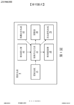
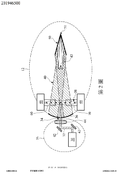
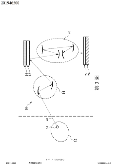
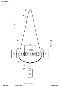
Extreme Ultra-Violet Apparatus and method of preventing EUV source device from contamination
PatentActiveTW201946500A
Innovation
- Implementing a gas barrier around the droplet stream in the EUV light source device using a gas injection system and vacuum exhaust system to contain evaporated particles, combined with component biasing to repel or attract charged particles, thereby reducing contamination.
Removal of contaminants from EUV masks
PatentActiveUS12019368B2
Innovation
- An aqueous cleaning composition comprising sulfonic acids or their salts, chloride ions, optionally an oxidizing agent, and a surfactant is used to effectively remove tin and other contaminants from EUV masks without damaging structural components like tantalum-based absorbers and anti-reflective coatings.
Regulatory Compliance Framework for EUV Systems
The regulatory landscape for EUV lithography systems encompasses a complex framework of international standards, national regulations, and industry-specific requirements. At the global level, organizations such as the International Organization for Standardization (ISO) and the International Electrotechnical Commission (IEC) have established foundational standards that govern the safety, quality, and performance aspects of semiconductor manufacturing equipment, including EUV systems.
Key regulatory frameworks include ISO 14644 for cleanroom environments, which is critical for EUV operations due to the extreme sensitivity of the lithography process to particulate contamination. Additionally, IEC 60601 series standards address electrical safety concerns, particularly relevant given the high-power laser systems and electrical components in EUV lithography tools.
Regional regulatory bodies impose their own compliance requirements. The European Union's Machinery Directive 2006/42/EC and Electromagnetic Compatibility Directive 2014/30/EU directly impact EUV system design and operation within EU member states. Similarly, the U.S. Occupational Safety and Health Administration (OSHA) regulations and the Semiconductor Equipment and Materials International (SEMI) standards provide comprehensive guidelines for equipment safety and operational protocols in North America.
Radiation safety represents a particularly critical aspect of EUV compliance. The International Atomic Energy Agency (IAEA) and national radiation protection agencies establish dose limits and shielding requirements for equipment that generates ionizing radiation. EUV systems must incorporate sophisticated radiation containment measures and monitoring systems to ensure operator safety and environmental protection.
Chemical safety regulations, including REACH in Europe and various chemical management laws globally, govern the handling of process chemicals used in EUV lithography. These regulations mandate proper storage, usage protocols, and disposal procedures for hazardous substances involved in the lithography process.
Quality management systems certification, particularly ISO 9001 and the more specialized IATF 16949 for automotive semiconductor applications, provides a structured approach to ensuring consistent quality in EUV system manufacturing and operation. These frameworks require rigorous documentation, process validation, and continuous improvement methodologies.
Compliance verification involves extensive testing and certification processes conducted by accredited third-party organizations. These assessments evaluate not only the technical performance of EUV systems but also their adherence to safety protocols, environmental standards, and quality management requirements. The certification process typically includes design review, risk assessment, performance testing, and on-site audits of manufacturing facilities.
Environmental Impact Assessment of EUV Processes
The environmental impact of Extreme Ultraviolet (EUV) lithography processes requires comprehensive assessment due to the technology's sophisticated nature and potential ecological footprint. EUV systems utilize high-powered lasers and tin droplets to generate the necessary 13.5nm wavelength light, creating concerns regarding energy consumption, waste generation, and chemical usage that must be evaluated against international environmental standards.
Energy consumption represents one of the most significant environmental considerations for EUV lithography. Current EUV systems require approximately 500kW of power during operation, substantially exceeding the energy demands of previous lithography technologies. This increased energy footprint necessitates careful evaluation of carbon emissions and implementation of energy efficiency measures to align with global sustainability goals and carbon reduction commitments.
Chemical management within EUV processes presents another critical environmental dimension. The technology employs various specialized chemicals including photoresists, developers, and cleaning agents. Many of these substances contain potentially hazardous components that require stringent handling protocols, specialized disposal methods, and comprehensive lifecycle management to prevent environmental contamination and ensure compliance with regulations such as EU REACH and RoHS directives.
Water usage and wastewater management constitute significant environmental considerations in EUV implementation. The process requires ultra-pure water for cleaning and cooling purposes, with a typical EUV facility consuming thousands of gallons daily. The resulting wastewater contains trace metals, chemical compounds, and particulates that necessitate advanced treatment systems to meet discharge regulations and minimize impact on local water resources.
Atmospheric emissions from EUV processes, while limited compared to traditional manufacturing, still warrant careful monitoring. The technology produces minimal particulate matter but generates gaseous byproducts including hydrogen and trace amounts of volatile organic compounds. These emissions must be captured through specialized filtration systems and abatement technologies to ensure compliance with air quality standards such as those established by the EPA and European Commission.
Waste management represents a final critical component of EUV environmental assessment. The technology generates various waste streams including used photoresist materials, contaminated filters, and replaced components containing rare earth elements. Implementing circular economy principles through recycling programs for valuable materials and proper disposal of hazardous waste is essential for minimizing environmental impact and meeting international waste management standards.
Unlock deeper insights with Patsnap Eureka Quick Research — get a full tech report to explore trends and direct your research. Try now!
Generate Your Research Report Instantly with AI Agent
Supercharge your innovation with Patsnap Eureka AI Agent Platform!