Understanding the Intersections of EUV Lithography and IoT Solutions
OCT 14, 20259 MIN READ
Generate Your Research Report Instantly with AI Agent
Patsnap Eureka helps you evaluate technical feasibility & market potential.
EUV Lithography and IoT Evolution Background
Extreme Ultraviolet (EUV) lithography represents a revolutionary advancement in semiconductor manufacturing, enabling the production of increasingly miniaturized and powerful integrated circuits. The technology's evolution began in the 1990s as researchers sought alternatives to traditional optical lithography, which was approaching its physical limits. By utilizing extremely short wavelengths (13.5 nm), EUV lithography has enabled the semiconductor industry to continue following Moore's Law, producing transistors at the 7nm node and below.
The Internet of Things (IoT), meanwhile, has evolved from a conceptual framework in the late 1990s to a ubiquitous technological ecosystem connecting billions of devices worldwide. The IoT evolution has been characterized by increasing device miniaturization, enhanced computational capabilities, improved energy efficiency, and expanded connectivity options. This progression has been fundamentally dependent on advancements in semiconductor manufacturing technologies.
The intersection of these two technological domains represents a fascinating symbiotic relationship. EUV lithography enables the production of more powerful, energy-efficient chips that serve as the foundation for advanced IoT devices. Conversely, the explosive growth of IoT applications creates unprecedented demand for semiconductor components, driving further innovation in manufacturing technologies like EUV lithography.
Historically, semiconductor manufacturing has followed a predictable trajectory of miniaturization, with each new generation enabling more transistors per chip. However, as feature sizes approached the 10nm threshold, traditional deep ultraviolet (DUV) lithography techniques encountered fundamental physical limitations. EUV lithography emerged as the solution to these challenges, though its implementation required overcoming significant technical hurdles related to light sources, masks, and resists.
The IoT landscape has simultaneously undergone dramatic transformation. Early IoT implementations were limited by processing power, energy consumption, and connectivity constraints. As semiconductor technology advanced, IoT capabilities expanded exponentially, enabling applications ranging from consumer wearables to industrial automation systems and smart city infrastructure.
Current trends indicate continued convergence between these technologies. EUV lithography is enabling the development of specialized IoT chips that combine processing capabilities, connectivity, and sensor integration in increasingly compact form factors. Meanwhile, the data generated by billions of IoT devices is driving demand for more powerful edge and cloud computing solutions, which in turn rely on advanced semiconductor manufacturing.
Understanding this technological co-evolution is essential for anticipating future developments in both fields. As EUV lithography continues to mature and new complementary technologies emerge, the capabilities of IoT devices will expand accordingly, enabling novel applications across diverse sectors including healthcare, transportation, manufacturing, and consumer electronics.
Market Demand Analysis for EUV-IoT Integration
The integration of Extreme Ultraviolet (EUV) lithography and Internet of Things (IoT) technologies represents a significant market opportunity across multiple sectors. Current market analysis indicates growing demand for advanced semiconductor manufacturing capabilities that can support the expanding IoT ecosystem. The global IoT market is projected to reach several trillion dollars by 2025, with connected devices numbering in the tens of billions, all requiring increasingly sophisticated semiconductor components.
EUV lithography, as the most advanced semiconductor manufacturing technology, enables the production of chips with feature sizes below 7nm. This capability directly addresses the market need for more powerful, energy-efficient processors and memory components essential for next-generation IoT devices. Market research shows particular demand growth in edge computing applications, where processing capabilities must be balanced with power consumption constraints.
Industry surveys reveal that manufacturers of IoT devices across automotive, industrial, healthcare, and consumer sectors are actively seeking semiconductor solutions that offer higher performance in smaller form factors. The automotive sector specifically demonstrates strong demand for EUV-enabled semiconductor components that can withstand harsh environments while delivering advanced driver assistance systems (ADAS) and autonomous driving capabilities.
Healthcare represents another significant market opportunity, with demand for implantable and wearable IoT devices requiring ultra-miniaturized, low-power components that can only be manufactured using advanced lithography techniques. Market forecasts indicate double-digit growth in this segment over the next five years.
From a geographical perspective, Asia-Pacific currently leads in demand for EUV-IoT integration, driven by the concentration of semiconductor manufacturing facilities and IoT device assembly operations. However, North America shows the fastest growth rate in specialized applications requiring cutting-edge semiconductor capabilities, particularly in defense, aerospace, and advanced medical devices.
Supply chain analysis indicates potential bottlenecks in meeting market demand, as EUV lithography equipment remains limited in availability and requires significant capital investment. This creates a premium market segment where manufacturers with access to EUV capabilities can command higher margins for IoT-specific semiconductor components.
Consumer willingness to pay for advanced IoT functionality enabled by EUV-manufactured components varies significantly by application. Mission-critical industrial and healthcare applications demonstrate the highest price tolerance, while consumer devices face more stringent cost constraints despite requiring advanced functionality.
Market timing analysis suggests that the convergence of EUV manufacturing capabilities and IoT market demand is approaching an inflection point, with significant growth expected as EUV manufacturing capacity expands and IoT applications continue to proliferate across industries.
Technical Challenges in EUV-IoT Convergence
The integration of Extreme Ultraviolet (EUV) lithography and Internet of Things (IoT) technologies presents significant technical challenges despite their potential synergistic benefits. The fundamental complexity arises from the vastly different scales and operational environments these technologies inhabit. EUV lithography operates at the nanometer scale in highly controlled cleanroom environments, while IoT systems function across diverse real-world settings with varying environmental conditions.
One primary challenge is the development of robust sensor networks capable of monitoring the intricate EUV lithography processes without introducing contamination. The extreme sensitivity of EUV systems to particulates smaller than 10nm requires sensors with unprecedented precision while maintaining compatibility with the vacuum and radiation environment of EUV chambers. Current IoT sensor technologies struggle to meet these stringent requirements while maintaining reliability.
Data management presents another substantial hurdle. EUV lithography systems generate massive volumes of process data—potentially terabytes per day from a single tool. Transmitting, processing, and analyzing this data in real-time through IoT frameworks demands advanced edge computing solutions and specialized communication protocols that can handle both the volume and security requirements of semiconductor manufacturing environments.
Power constraints significantly impact the integration efforts. EUV systems consume substantial energy, while many IoT devices are designed for low-power operation. Developing energy-efficient monitoring solutions that can operate continuously in proximity to EUV equipment without requiring frequent maintenance or battery replacement remains technically challenging.
Security vulnerabilities emerge at the intersection of these technologies. The semiconductor industry requires exceptional protection of intellectual property and manufacturing processes. Introducing IoT connectivity to EUV systems creates potential attack vectors that must be addressed through specialized security frameworks beyond standard IoT security protocols.
Thermal management issues arise when integrating electronic IoT components near EUV systems that generate significant heat. Ensuring reliable operation of sensors and communication modules in these environments requires advanced thermal design and materials science solutions not commonly found in conventional IoT deployments.
Standardization gaps between semiconductor manufacturing protocols and IoT communication standards create interoperability challenges. The semiconductor industry uses specialized interfaces and protocols (SECS/GEM, etc.) that must be bridged to common IoT standards (MQTT, CoAP) through complex middleware solutions, adding layers of complexity to system integration.
The technical expertise divide between semiconductor engineering specialists and IoT developers further complicates integration efforts. Cross-disciplinary knowledge is rare, creating communication barriers and implementation challenges when teams attempt to merge these technologies into cohesive solutions.
Current EUV-IoT Integration Solutions
01 EUV Lithography Systems and Components
Extreme Ultraviolet (EUV) lithography systems utilize short wavelength light to create nanometer-scale patterns on semiconductor wafers. These systems include specialized components such as mirrors, masks, and light sources that operate in vacuum environments. The technology enables the production of smaller, more densely packed integrated circuits with feature sizes below 10nm, which is crucial for advancing semiconductor manufacturing capabilities.- EUV Lithography Systems and Components: Extreme Ultraviolet (EUV) lithography systems utilize short wavelength light to create nanometer-scale patterns on semiconductor wafers. These systems include specialized components such as mirrors, masks, and light sources that operate in vacuum environments. The technology enables the production of smaller, more densely packed integrated circuits with feature sizes below 10nm, supporting continued advancement in semiconductor manufacturing capabilities.
- IoT Device Integration with Semiconductor Manufacturing: Internet of Things (IoT) solutions are being integrated into semiconductor manufacturing processes, including EUV lithography. These solutions involve networks of sensors that monitor equipment performance, environmental conditions, and process parameters in real-time. The collected data enables predictive maintenance, process optimization, and quality control, resulting in improved manufacturing efficiency and reduced downtime.
- Advanced Process Control for EUV Lithography: Advanced process control systems for EUV lithography incorporate machine learning algorithms and real-time data analysis to optimize exposure parameters, alignment, and focus. These systems can automatically adjust process variables based on feedback from integrated sensors and metrology tools, compensating for variations in equipment performance and environmental conditions to maintain consistent pattern quality across wafers.
- EUV Resist Materials and Processing: Specialized photoresist materials have been developed specifically for EUV lithography applications. These materials are designed to be highly sensitive to EUV radiation while providing the resolution and pattern fidelity required for advanced semiconductor nodes. The processing of these resists involves precise control of development conditions, post-exposure baking, and etching parameters to achieve optimal pattern transfer.
- Edge Computing Solutions for Lithography Systems: Edge computing architectures are being implemented in EUV lithography systems to process the massive amounts of data generated during semiconductor manufacturing. These solutions enable real-time analysis and decision-making at the equipment level, reducing latency and bandwidth requirements. Edge computing nodes can perform complex calculations for mask optimization, dose control, and pattern verification without relying on centralized computing resources.
02 EUV Process Control and Optimization
Methods and systems for controlling and optimizing EUV lithography processes focus on improving accuracy, throughput, and yield. These include advanced metrology techniques, real-time monitoring systems, and feedback control mechanisms that adjust process parameters based on measured results. Process optimization strategies address challenges such as pattern fidelity, overlay accuracy, and defect reduction to ensure consistent manufacturing quality.Expand Specific Solutions03 IoT Integration in Semiconductor Manufacturing
Internet of Things (IoT) solutions are being integrated into semiconductor manufacturing environments to enhance production efficiency and equipment monitoring. These systems collect and analyze data from various manufacturing tools, including EUV lithography equipment, to enable predictive maintenance, process optimization, and quality control. IoT platforms facilitate real-time decision making and remote monitoring capabilities across fabrication facilities.Expand Specific Solutions04 Advanced Mask Technology for EUV
Specialized mask technologies for EUV lithography address unique challenges associated with short wavelength exposure. These include reflective masks with multilayer coatings, advanced absorber materials, and novel designs to mitigate pattern distortion effects. Mask inspection and repair techniques ensure defect-free patterns, while computational approaches optimize mask designs for specific applications to achieve desired pattern transfer accuracy.Expand Specific Solutions05 EUV and IoT for Smart Manufacturing
The convergence of EUV lithography and IoT creates opportunities for smart manufacturing in the semiconductor industry. This integration enables data-driven production environments where equipment performance, process parameters, and quality metrics are continuously monitored and optimized. Advanced analytics and machine learning algorithms process the collected data to identify patterns, predict failures, and suggest process improvements, leading to higher yields and reduced downtime.Expand Specific Solutions
Key Industry Players in EUV and IoT Sectors
The EUV lithography and IoT solutions market is in a growth phase, with increasing integration between advanced semiconductor manufacturing and connected device ecosystems. The global market is expanding rapidly, driven by demand for smaller, more powerful chips for IoT applications. Technologically, EUV lithography is maturing with ASML holding dominant position in equipment manufacturing, while Taiwan Semiconductor, Samsung, and Intel lead in implementation. Companies like Huawei, ZTE, and Siemens are bridging semiconductor capabilities with IoT applications. Research institutions such as Beijing University of Posts & Telecommunications and Tongji University are advancing theoretical foundations. The competitive landscape features established semiconductor giants collaborating with software and connectivity providers to create comprehensive solutions for the converging EUV-IoT ecosystem.
Taiwan Semiconductor Manufacturing Co., Ltd.
Technical Solution: TSMC has developed a sophisticated approach to integrating EUV lithography with IoT solutions across their manufacturing facilities. Their "Intelligent Fab" initiative incorporates over 50,000 IoT sensors throughout their EUV production lines, creating a comprehensive digital twin of their manufacturing operations. TSMC utilizes advanced analytics to optimize EUV exposure parameters in real-time, achieving up to 15% improvement in throughput compared to traditional methods. Their system employs machine learning algorithms that continuously analyze process data from EUV lithography tools to predict maintenance needs and prevent costly downtime. TSMC has implemented edge computing nodes directly connected to their EUV systems, processing over 30TB of data daily to enable immediate adjustments to lithography parameters based on environmental conditions and previous exposure results, significantly enhancing yield rates for their most advanced process nodes.
Strengths: Industry-leading implementation of IoT in semiconductor manufacturing; extensive experience as primary user of EUV technology; proven track record of yield improvements through data-driven optimization. Weaknesses: Proprietary systems limiting broader industry adoption; high capital investment requirements; dependency on equipment suppliers like ASML for core EUV technology advancements.
Intel Corp.
Technical Solution: Intel has developed an integrated approach to EUV lithography and IoT called "Smart Lithography Platform" (SLP). This system incorporates thousands of sensors throughout their EUV lithography process, collecting data on over 200 critical parameters including temperature variations, vibration levels, and optical performance metrics. Intel's platform utilizes edge computing nodes positioned directly within their fabrication facilities to process approximately 25TB of data daily with latency under 10ms for time-critical adjustments. Their proprietary algorithms analyze patterns across multiple EUV exposure cycles to identify subtle variations that could impact yield, enabling proactive adjustments before defects occur. Intel has implemented a hierarchical IoT architecture specifically designed for their EUV operations, with localized processing for immediate control decisions and cloud integration for deeper analytics and cross-fab optimization. This approach has reportedly reduced EUV-related defects by approximately 35% while improving equipment utilization rates by 12-15% compared to their previous systems.
Strengths: Vertical integration allowing seamless hardware-software optimization; extensive manufacturing expertise informing practical IoT implementations; strong internal research capabilities. Weaknesses: Relatively late adoption of EUV technology compared to competitors; challenges in scaling IoT solutions across diverse manufacturing facilities; complex legacy systems integration issues.
Critical Patents and Research in EUV-IoT Intersection
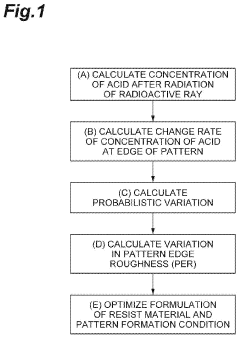
Method of simulating resist pattern, resist material and method of optimizing formulation thereof, apparatus and recording medium
PatentActiveUS20200057371A1
Innovation
- A simulation method and resist material formulation optimization that accounts for probabilistic variations in photon noise and active species distribution, using a chemical amplification-type resist material with a photo-acid-generating agent and photodecomposable quencher, to minimize pattern edge roughness and sensitivity variations.
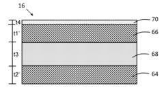
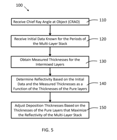
Extreme ultraviolet mirrors and masks with improved reflectivity
PatentInactiveUS20180226166A1
Innovation
- A method to optimize the reflectivity of multi-layer stacks in EUV optical elements by determining and selecting the thicknesses of intermixed and pure layers to maximize reflectivity, using a computer-based system that considers intermixing and deposition conditions, and implementing these optimizations in Bragg mirrors and masks.
Supply Chain Implications for EUV-IoT Technologies
The integration of EUV lithography and IoT technologies creates complex supply chain dynamics that require careful consideration. The specialized nature of EUV equipment, particularly the advanced optical systems and precision components, necessitates a highly specialized supplier network that spans multiple continents. Key suppliers like ASML, Zeiss, and Cymer form the backbone of this ecosystem, creating potential bottlenecks and single points of failure that could impact global semiconductor production.
Material sourcing presents significant challenges, particularly for rare earth elements and specialized chemicals required for both EUV processes and IoT sensor manufacturing. The geographical concentration of these resources in regions like China for rare earth elements and Japan for photoresist chemicals introduces geopolitical vulnerabilities that can disrupt the entire supply chain. Recent global events have highlighted these vulnerabilities, prompting industry leaders to explore alternative sourcing strategies and material substitutions.
Logistics and transportation for EUV-IoT technologies demand exceptional precision. EUV lithography machines, weighing several tons and containing thousands of precision components, require specialized transportation solutions with vibration control and environmental stability. Similarly, many IoT components require controlled environments during shipping to maintain their integrity and functionality.
Inventory management strategies are evolving to address the unique challenges of this intersection. Just-in-time approaches are being reconsidered in favor of strategic stockpiling of critical components, particularly those with limited supplier options or long lead times. Advanced analytics and IoT-enabled tracking systems are being deployed to provide real-time visibility into inventory levels and supply chain movements.
Resilience planning has become a central focus for companies operating in this space. Diversification of suppliers, development of alternative materials, and investment in localized production capabilities are emerging as key strategies. The concept of "friendshoring" – establishing supply relationships with geopolitically aligned nations – is gaining traction as companies seek to reduce vulnerability to international tensions.
The environmental impact of these supply chains is receiving increased scrutiny. The significant energy requirements of EUV lithography and the electronic waste generated by IoT devices present sustainability challenges that must be addressed. Leading companies are investing in circular economy initiatives, including component reuse programs and more environmentally friendly manufacturing processes, to mitigate these impacts while maintaining the technological advancement necessary for continued innovation.
Sustainability Considerations in EUV-IoT Development
The integration of EUV lithography and IoT solutions presents significant sustainability challenges and opportunities that must be addressed as these technologies continue to converge. The energy-intensive nature of EUV lithography processes, which require substantial power for generating and directing extreme ultraviolet light, raises important environmental concerns. Current EUV systems consume between 500-1000 kW during operation, contributing significantly to the semiconductor industry's carbon footprint.
Water usage represents another critical sustainability consideration, with EUV lithography requiring ultra-pure water for cooling systems and cleaning processes. A typical advanced semiconductor fabrication facility utilizing EUV technology may consume 4-7 million gallons of water daily, necessitating innovative water recycling and conservation approaches when integrating with IoT manufacturing processes.
Material efficiency and waste reduction present both challenges and opportunities in the EUV-IoT intersection. The rare and expensive materials used in EUV systems, including specialized mirrors coated with molybdenum-silicon multilayers, demand responsible sourcing and end-of-life management strategies. IoT integration can potentially optimize material usage through real-time monitoring and predictive maintenance, reducing waste and extending component lifespans.
Energy optimization through IoT implementation offers promising sustainability benefits. Smart sensors and AI-driven control systems can monitor and adjust EUV lithography processes in real-time, potentially reducing energy consumption by 15-25% compared to conventional systems. These efficiency gains become increasingly significant as EUV technology scales to meet growing semiconductor demands for IoT device production.
Circular economy principles are gradually being applied to EUV-IoT development, with manufacturers implementing take-back programs for specialized components and exploring remanufacturing options. The semiconductor industry has established targets to increase recycling rates of critical materials from current levels of approximately 30% to over 60% by 2030, though significant technical challenges remain in recovering high-purity materials from complex EUV systems.
Regulatory frameworks worldwide are evolving to address the environmental impacts of advanced semiconductor manufacturing. The European Union's Eco-Design Directive and various international agreements on greenhouse gas emissions are increasingly influencing how EUV and IoT technologies are developed and deployed, creating both compliance challenges and incentives for sustainable innovation in this rapidly evolving technological intersection.
Unlock deeper insights with Patsnap Eureka Quick Research — get a full tech report to explore trends and direct your research. Try now!
Generate Your Research Report Instantly with AI Agent
Supercharge your innovation with Patsnap Eureka AI Agent Platform!