

EUV Lithography: A Benchmark Study for Photonic Circuitry
OCT 14, 202510 MIN READ
Generate Your Research Report Instantly with AI Agent
PatSnap Eureka helps you evaluate technical feasibility & market potential.
EUV Lithography Evolution and Objectives
Extreme Ultraviolet (EUV) lithography represents a revolutionary advancement in semiconductor manufacturing technology, marking a significant departure from traditional optical lithography methods. The evolution of EUV lithography began in the late 1980s when researchers recognized the limitations of conventional deep ultraviolet (DUV) lithography in achieving smaller feature sizes. The technology utilizes 13.5 nm wavelength light, enabling the production of semiconductor devices with feature sizes below 10 nm.
The historical trajectory of EUV lithography development has been characterized by persistent technical challenges and collaborative industry efforts. Initial research focused on fundamental physics and proof-of-concept demonstrations, followed by the development of practical EUV light sources, specialized optics, and photoresist materials. By the early 2000s, consortia like SEMATECH and ASML's partnerships with research institutions accelerated progress toward commercial viability.
A critical milestone occurred in 2018 when ASML delivered the first production-ready EUV lithography systems to leading semiconductor manufacturers. This achievement represented the culmination of over three decades of research and development, with investments exceeding $10 billion. The technology has since enabled the continuation of Moore's Law beyond what was previously thought possible with conventional lithography techniques.
In the context of photonic circuitry, EUV lithography offers unprecedented precision for fabricating nanophotonic components. The technology enables the creation of waveguides, resonators, and other photonic structures with dimensions approaching the wavelength of light used in optical communications. This capability is essential for advancing integrated photonics, which promises to overcome the bandwidth and energy efficiency limitations of electronic circuits.
The primary objectives of EUV lithography in photonic applications include achieving sub-10 nm feature sizes with high throughput, reducing pattern edge roughness to minimize optical losses, and ensuring compatibility with existing semiconductor manufacturing processes. Additionally, researchers aim to develop specialized EUV resists optimized for photonic structures, which have different requirements than electronic components.
Looking forward, the technology roadmap for EUV lithography includes high-numerical-aperture (high-NA) EUV systems capable of resolving features below 8 nm, multi-patterning techniques to further extend resolution limits, and computational lithography approaches that optimize pattern fidelity. These advancements are critical for enabling next-generation photonic integrated circuits that will form the backbone of future computing and communication systems.
Market Demand for Advanced Photonic Circuitry
The global market for advanced photonic circuitry is experiencing unprecedented growth, driven primarily by the increasing demand for high-speed data transmission, energy-efficient computing solutions, and miniaturized electronic components. As traditional electronic circuits approach their physical limitations in terms of speed and energy efficiency, photonic integrated circuits (PICs) have emerged as a promising alternative, offering superior performance in data processing and transmission.
The telecommunications sector represents the largest market segment for advanced photonic circuitry, with an estimated annual growth rate exceeding 20% over the past five years. This surge is primarily attributed to the exponential increase in global data traffic, necessitating higher bandwidth and more efficient data transmission technologies. Major telecom operators worldwide are actively investing in photonic technologies to enhance their network infrastructure capabilities.
Data centers constitute another significant market for photonic circuitry, as they seek to reduce power consumption while increasing data processing speeds. The energy efficiency advantages of photonic circuits compared to traditional electronic circuits make them particularly attractive for large-scale computing facilities, where power consumption represents a substantial operational cost. Several leading cloud service providers have already begun implementing photonic interconnects in their newest data center designs.
Consumer electronics manufacturers are also showing increased interest in photonic circuitry, particularly for applications requiring high-speed data transfer such as augmented reality devices, high-definition displays, and next-generation smartphones. Market research indicates that consumer applications could potentially become the fastest-growing segment for photonic circuitry within the next decade.
The automotive industry represents an emerging market for advanced photonic circuitry, particularly with the development of autonomous vehicles that require sophisticated sensing and communication systems. LiDAR systems, which rely heavily on photonic components, are becoming standard features in advanced driver-assistance systems, creating substantial demand for specialized photonic circuits.
EUV lithography plays a crucial role in meeting these market demands by enabling the production of increasingly miniaturized and complex photonic circuits. The precision offered by EUV technology allows for the fabrication of nanoscale photonic components with unprecedented accuracy, directly addressing the industry's need for higher integration density and improved performance.
Market forecasts suggest that the global photonic integrated circuit market will continue its robust growth trajectory, potentially reaching a market value several times its current size by 2030. This growth is expected to accelerate as EUV lithography technology matures, reducing production costs and enabling more widespread adoption of photonic circuitry across various industries.
EUV Technology Status and Implementation Barriers
Extreme Ultraviolet (EUV) lithography represents a revolutionary advancement in semiconductor manufacturing technology, enabling the production of increasingly miniaturized integrated circuits. Currently, EUV lithography has reached commercial implementation in leading semiconductor fabrication facilities, with ASML holding a virtual monopoly on EUV lithography systems. The technology operates at a wavelength of 13.5nm, significantly shorter than previous deep ultraviolet (DUV) systems that operated at 193nm, allowing for much finer feature resolution.
Despite its commercial deployment, EUV technology faces substantial implementation barriers that limit its broader adoption across the semiconductor industry. The most significant challenge remains the extraordinarily high cost of EUV lithography systems, with each machine priced at approximately $150-200 million. This represents a capital investment that only the largest semiconductor manufacturers can justify, creating a significant barrier to entry for smaller players in the market.
Technical challenges persist in EUV power source stability and efficiency. Current EUV systems utilize laser-produced plasma sources that generate EUV radiation by firing high-power CO2 lasers at tin droplets. These sources still struggle to maintain consistent power levels needed for high-volume manufacturing, with typical source power around 250W when industry targets for optimal throughput require 500W or higher. This power limitation directly impacts production throughput and economic viability.
Mask defectivity remains another critical barrier. EUV masks are significantly more complex than traditional photomasks, utilizing multilayer reflective coatings rather than transmissive designs. The absence of pellicles (protective films) that can withstand EUV radiation intensities creates vulnerability to particle contamination. Additionally, mask inspection tools capable of detecting defects at EUV-relevant dimensions remain limited in capability and extremely expensive.
Photoresist performance continues to challenge implementation efforts. EUV photoresists must simultaneously achieve high sensitivity (to compensate for limited source power), low line edge roughness, and minimal pattern collapse at extremely small dimensions. The stochastic effects at these dimensions create fundamental physical limitations that resist manufacturers are still working to overcome.
For photonic circuitry applications specifically, EUV lithography faces additional challenges related to the three-dimensional nature of photonic structures. While EUV excels at creating extremely fine two-dimensional patterns, photonic circuits often require precise control of sidewall angles and feature heights that extend beyond traditional semiconductor requirements. The integration of these capabilities into EUV processes represents an ongoing area of development.
Infrastructure requirements present another significant barrier, with EUV systems requiring specialized facilities with extraordinary vibration control, temperature stability, and vacuum systems. The complexity of maintenance and operation further limits deployment to only the most sophisticated manufacturing environments.
Current EUV Solutions for Photonic Circuit Fabrication
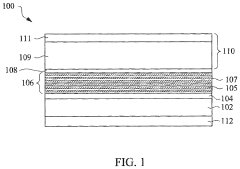
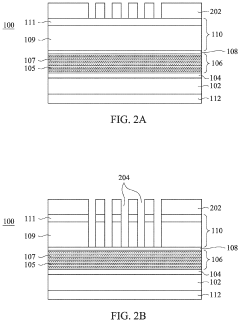
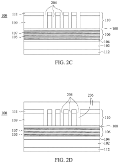
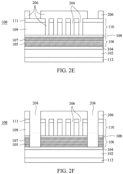
01 EUV lithography system components and design
EUV lithography systems incorporate specialized components designed to work with extreme ultraviolet light. These systems typically include radiation sources, optical elements, mirrors, and projection systems that operate in vacuum environments. The design focuses on managing the short wavelength radiation to achieve high-resolution patterning for semiconductor manufacturing, with particular attention to optical alignment and beam path optimization.- EUV Lithography System Components: EUV lithography systems consist of specialized components designed to work with extreme ultraviolet light. These include EUV light sources, reflective optics (since EUV is absorbed by traditional lenses), specialized masks, and precision positioning systems. The systems operate in vacuum environments as EUV light is absorbed by air. Advanced sensors and control systems ensure nanometer-level accuracy required for semiconductor manufacturing at extremely small feature sizes.
- EUV Source Technology: EUV light sources typically generate extreme ultraviolet radiation at 13.5nm wavelength through laser-produced plasma or discharge-produced plasma methods. These sources use tin, xenon or other materials that emit EUV radiation when excited to high energy states. The technology includes sophisticated debris mitigation systems, collector optics, and power delivery systems to provide stable, high-power EUV light required for high-volume manufacturing applications.
- EUV Mask Technology: EUV masks differ significantly from traditional photomasks, using reflective rather than transmissive designs. They consist of multilayer mirrors with patterned absorber layers that reflect EUV radiation in specific patterns. The technology includes advanced materials for high reflectivity, defect inspection and repair methods, and pellicle solutions to protect masks from contamination. Mask architecture must account for unique challenges like shadowing effects and three-dimensional pattern fidelity at extreme scales.
- EUV Process Control and Optimization: Process control for EUV lithography requires specialized techniques to manage the unique challenges of working with EUV radiation. This includes advanced computational lithography methods, overlay control systems, and focus control mechanisms. The technology encompasses sophisticated metrology tools for measuring critical dimensions, defect inspection systems, and feedback loops for process optimization. Machine learning algorithms are increasingly employed to enhance process control and yield management in EUV lithography.
- EUV Resist and Pattern Development: EUV-specific photoresist materials are designed to be highly sensitive to EUV radiation while maintaining the resolution, line edge roughness, and sensitivity requirements for advanced semiconductor nodes. These specialized chemical formulations include novel polymer systems, photoacid generators, and quencher components optimized for EUV wavelengths. The technology also encompasses post-exposure development processes, pattern transfer techniques, and methods to minimize stochastic effects that become prominent at extreme dimensions.
02 Contamination control and mitigation in EUV systems
Contamination control is critical in EUV lithography due to the sensitivity of optical components to particles and molecular contaminants. Various techniques are employed to prevent and mitigate contamination, including specialized cleaning methods, protective layers for optical surfaces, gas purging systems, and contamination barriers. These approaches help maintain system performance and extend the lifetime of critical components exposed to intense EUV radiation.Expand Specific Solutions03 EUV mask technology and inspection
EUV masks require specialized materials and structures to effectively pattern semiconductor devices at extreme ultraviolet wavelengths. These masks typically use reflective rather than transmissive designs and incorporate multiple layers for optimal performance. Advanced inspection techniques are employed to detect defects and ensure pattern fidelity, including actinic inspection methods that use EUV wavelengths to identify issues that might not be visible with conventional inspection approaches.Expand Specific Solutions04 Thermal management in EUV lithography
Thermal management is essential in EUV lithography systems due to the high energy levels involved. The absorption of EUV radiation generates significant heat that can cause thermal expansion, distortion, and degradation of critical components. Advanced cooling systems, temperature monitoring, and thermal compensation mechanisms are implemented to maintain dimensional stability and ensure consistent imaging performance during operation.Expand Specific Solutions05 Computational methods for EUV lithography optimization
Computational techniques play a crucial role in optimizing EUV lithography processes. These include simulation methods for predicting imaging performance, optical proximity correction algorithms to enhance pattern fidelity, and machine learning approaches to improve process control. Design rule checking and verification tools are also employed to ensure that patterns can be successfully transferred using EUV technology, accounting for the unique challenges of short-wavelength lithography.Expand Specific Solutions
Leading Companies in EUV Lithography Ecosystem
EUV Lithography for photonic circuitry is currently in an early growth phase, with the market expected to expand significantly as demand for advanced semiconductor manufacturing increases. The global market is projected to reach $10-15 billion by 2025, driven by the need for smaller, more efficient chip designs. Technologically, ASML Holding NV maintains market leadership with its proprietary EUV systems, while Taiwan Semiconductor Manufacturing Co. and Samsung Electronics are the primary adopters implementing this technology at scale. Other key players developing complementary technologies include Tokyo Electron, Lam Research, and Carl Zeiss SMT. IBM and GlobalFoundries are advancing research applications, while Chinese entities like Shanghai Micro Electronics Equipment are working to close the technological gap. The ecosystem remains highly concentrated with significant barriers to entry due to the complex technical requirements.
Taiwan Semiconductor Manufacturing Co., Ltd.
Technical Solution: TSMC has pioneered the implementation of EUV lithography in high-volume semiconductor manufacturing, particularly for advanced nodes below 7nm. Their N7+ technology was the first commercially available process to use EUV, reducing mask layers by 20% compared to traditional DUV approaches. TSMC's N5 process extensively leverages EUV lithography for critical layers, achieving approximately 1.8x logic density improvement over N7. Their EUV implementation strategy focuses on selective layer application where EUV provides maximum economic benefit, typically for critical dimensions requiring single-exposure patterning. TSMC has developed specialized resist materials optimized for their process conditions, achieving line edge roughness below 2nm. Their photonic circuit applications include advanced silicon photonics platforms with waveguide losses below 0.5dB/cm and integrated germanium photodetectors with >30GHz bandwidth. TSMC's EUV implementation includes sophisticated computational lithography techniques and design-technology co-optimization methodologies to maximize pattern fidelity and yield[2][5].
Strengths: Industry-leading implementation of EUV in high-volume manufacturing; proven integration with advanced packaging technologies; extensive process control expertise; comprehensive design enablement ecosystem. Weaknesses: Extremely high capital expenditure requirements; dependency on limited EUV equipment suppliers; challenges with throughput optimization at leading nodes; ongoing work needed to reduce defect densities.
Samsung Electronics Co., Ltd.
Technical Solution: Samsung has aggressively adopted EUV lithography for its advanced semiconductor manufacturing processes, particularly in memory and logic applications. Their 7nm LPP (Low Power Plus) process was among the first to implement EUV technology, reducing mask complexity by approximately 20% compared to multi-patterning approaches. Samsung's EUV implementation extends to their V-NAND flash memory technology, where they've achieved sub-20nm cell structures with improved uniformity. For photonic circuitry applications, Samsung has developed specialized EUV processes achieving waveguide losses below 0.7dB/cm in silicon nitride platforms. Their approach combines EUV lithography with advanced etching techniques to create high-aspect-ratio waveguide structures with sidewall roughness below 1nm RMS. Samsung has invested in developing proprietary computational lithography solutions specifically optimized for photonic component manufacturing, addressing the unique challenges of curved structures and varying critical dimensions. Their research includes novel resist formulations with enhanced sensitivity (approximately 30mJ/cm²) while maintaining resolution capabilities below 15nm[4][6].
Strengths: Vertically integrated manufacturing capabilities; significant capital investment capacity; expertise across memory and logic applications; advanced packaging integration capabilities. Weaknesses: Relatively newer to EUV implementation compared to some competitors; ongoing yield optimization challenges; high operational costs; dependency on limited equipment suppliers.
Critical Patents and Breakthroughs in EUV Technology
Protection layer on low thermal expansion material (LTEM) substrate of extreme ultraviolet (EUV) mask
PatentActiveUS12001132B2
Innovation
- A protection layer is deposited on the LTEM substrate, functioning as an etch stop and reducing particle generation during EUV irradiation, while retaining some reflective multilayers to maintain high reflectivity and control critical dimension errors.
Alternating copolymer chain scission photoresists
PatentActiveUS11906901B2
Innovation
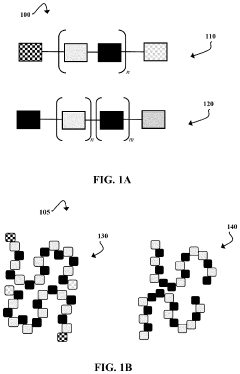
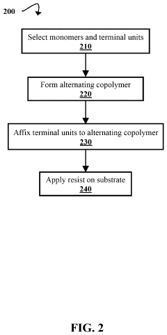
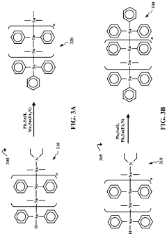
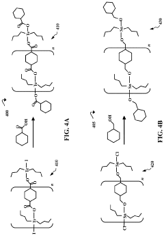
- Development of alternating copolymers with EUV-absorbing elements, such as Sn, Te, or Bi, that undergo chain scission upon EUV radiation exposure, eliminating the need for minority components like chemical amplifiers, and incorporating unreactive terminal units to control polymer chain lengths and prevent inter-chain reactions.
Environmental Impact of EUV Manufacturing Processes
The manufacturing processes associated with Extreme Ultraviolet (EUV) lithography present significant environmental considerations that must be addressed as this technology becomes more prevalent in photonic circuitry production. EUV systems require substantial energy inputs, with a single EUV lithography machine consuming approximately 1 megawatt of power during operation. This high energy demand contributes to considerable carbon emissions, particularly in regions where electricity generation relies heavily on fossil fuels.
Water usage represents another critical environmental concern. The production of EUV equipment and its operation necessitate ultra-pure water in substantial quantities for cooling systems and cleaning processes. A typical semiconductor fabrication facility utilizing EUV technology may consume millions of gallons of water daily, placing pressure on local water resources and requiring extensive water treatment infrastructure.
The rare materials required for EUV lithography components present additional environmental challenges. Critical elements such as ruthenium for mirrors and specialized materials for masks involve mining operations with significant ecological footprints. The extraction processes for these materials often generate toxic byproducts and can lead to habitat destruction in mining regions.
Chemical waste management constitutes a substantial environmental consideration in EUV manufacturing. The process utilizes various specialized chemicals, including photoresists, developers, and cleaning agents. Many of these substances are potentially hazardous and require sophisticated treatment protocols before disposal. Improper handling can lead to soil contamination and water pollution, necessitating rigorous waste management systems.
The production of EUV light sources generates specific environmental concerns. Tin droplet technology, commonly used in EUV systems, produces tin waste that requires specialized disposal methods. Additionally, the high-vacuum environments essential for EUV operation demand energy-intensive pumping systems that contribute to the overall environmental footprint.
Several leading semiconductor manufacturers have initiated sustainability programs specifically targeting EUV environmental impacts. These include closed-loop water recycling systems, energy efficiency improvements, and chemical recovery processes. ASML, the primary manufacturer of EUV equipment, has committed to carbon neutrality goals and implemented design modifications to reduce resource consumption in newer generation machines.
Regulatory frameworks governing EUV manufacturing environmental impacts vary globally, with the European Union typically enforcing the most stringent standards through directives like the Restriction of Hazardous Substances (RoHS) and Registration, Evaluation, Authorization and Restriction of Chemicals (REACH) regulations. As EUV adoption accelerates in photonic circuitry applications, harmonizing these regulatory approaches will become increasingly important for sustainable industry growth.
Supply Chain Resilience for EUV Equipment
The global supply chain for Extreme Ultraviolet (EUV) lithography equipment represents one of the most complex and vulnerable technological ecosystems in the semiconductor industry. With only a handful of suppliers capable of producing critical components, the EUV supply chain faces significant resilience challenges that could impact the advancement of photonic circuitry manufacturing.
ASML, the sole manufacturer of EUV lithography machines, relies on a network of specialized suppliers spanning multiple continents. The mirrors required for EUV systems, manufactured by Zeiss in Germany, demand unprecedented precision with surface irregularities less than 20 picometers. Similarly, the EUV light sources developed by Cymer (now an ASML subsidiary) in the United States require specialized components from global suppliers, creating multiple potential points of failure.
Geopolitical tensions have emerged as a primary threat to EUV supply chain stability. Export controls and technology restrictions between major semiconductor-producing nations have created uncertainty regarding access to critical components and intellectual property. The concentration of key suppliers in regions susceptible to natural disasters or political instability further compounds these vulnerabilities.
The COVID-19 pandemic exposed additional weaknesses in the EUV supply chain, with manufacturing delays and logistics disruptions affecting delivery schedules for new equipment. These delays directly impacted the development timeline for advanced photonic circuitry, highlighting the interconnectedness of global technology supply networks.
To enhance resilience, leading semiconductor manufacturers have implemented several strategic approaches. Intel, TSMC, and Samsung have established closer partnerships with ASML and key suppliers, including multi-year purchase agreements and joint technology development initiatives. These arrangements provide greater visibility into the supply chain and help stabilize component availability.
Geographical diversification of manufacturing capabilities represents another critical strategy. Several suppliers have established redundant production facilities in different regions to mitigate location-specific risks. This approach, while capital-intensive, provides essential backup capacity during regional disruptions.
Inventory management practices have also evolved, with many companies increasing safety stock levels of critical components despite the associated carrying costs. Advanced analytics and supply chain visibility tools enable more accurate forecasting and earlier detection of potential disruptions, allowing for proactive mitigation measures.
Looking forward, the industry is exploring opportunities to standardize certain components across different generations of EUV equipment, potentially reducing supply chain complexity and increasing the number of qualified suppliers. However, the highly specialized nature of EUV technology will continue to present unique challenges for supply chain resilience in photonic circuitry manufacturing.
Unlock deeper insights with PatSnap Eureka Quick Research — get a full tech report to explore trends and direct your research. Try now!
Generate Your Research Report Instantly with AI Agent
Supercharge your innovation with PatSnap Eureka AI Agent Platform!