EUV Lithography: Contributions to the Evolution of Smart Grid Electronics
OCT 14, 20259 MIN READ
Generate Your Research Report Instantly with AI Agent
Patsnap Eureka helps you evaluate technical feasibility & market potential.
EUV Lithography Background and Smart Grid Integration Goals
Extreme Ultraviolet (EUV) lithography represents a revolutionary advancement in semiconductor manufacturing technology, marking a significant departure from traditional deep ultraviolet (DUV) lithography methods. Developed over several decades, EUV lithography utilizes light with a wavelength of 13.5 nanometers, enabling the production of semiconductor components with feature sizes below 7 nanometers. This technological breakthrough has been pivotal in sustaining Moore's Law, which predicts the doubling of transistor density approximately every two years.
The evolution of EUV technology can be traced back to the early 1990s when researchers began exploring alternatives to conventional optical lithography. After overcoming numerous technical challenges related to light sources, mirrors, and photoresist materials, EUV lithography achieved commercial viability in the late 2010s. Companies like ASML, in collaboration with research institutions worldwide, have been instrumental in transforming EUV from a theoretical concept to a production-ready technology.
Smart grid systems, meanwhile, have emerged as the next generation of power infrastructure, integrating advanced digital communications, automated controls, and distributed energy resources. These systems require increasingly sophisticated electronics for functions such as real-time monitoring, adaptive protection, and grid optimization. As smart grids continue to evolve, the demand for more powerful, energy-efficient, and reliable semiconductor components has grown exponentially.
The integration of EUV lithography into smart grid electronics development represents a convergence of cutting-edge semiconductor manufacturing with advanced power systems. This integration aims to address several critical objectives: enhancing the computational capabilities of grid management systems, improving the energy efficiency of power electronics, and increasing the reliability of critical infrastructure components.
One primary goal of this technological synergy is to enable more sophisticated edge computing capabilities within smart grid networks. By leveraging the higher transistor densities made possible through EUV lithography, smart grid devices can process larger volumes of data locally, reducing latency and improving response times to grid disturbances.
Another objective is the miniaturization of power electronic components, particularly in applications such as solid-state transformers, advanced inverters, and high-voltage direct current (HVDC) systems. Smaller, more efficient components can significantly reduce energy losses throughout the grid while enabling more flexible deployment options.
Furthermore, the integration of EUV-manufactured semiconductors into smart grid systems aims to enhance resilience against electromagnetic interference and cyber threats. The increased integration density allows for more sophisticated security features and redundancy mechanisms to be incorporated directly into hardware components, providing an additional layer of protection for critical infrastructure.
Market Demand Analysis for Advanced Semiconductor Solutions in Smart Grids
The smart grid market is experiencing unprecedented growth, driven by the global push for energy efficiency, renewable integration, and grid modernization. Current market projections indicate that the global smart grid technology market will reach approximately $92 billion by 2026, growing at a CAGR of 17.4% from 2021. Within this ecosystem, advanced semiconductor solutions powered by EUV lithography technology are becoming increasingly critical components.
The demand for high-performance semiconductors in smart grid applications stems from several converging factors. Power management integrated circuits (PMICs), microcontrollers, and specialized ASICs are essential for enabling real-time monitoring, automated control systems, and efficient power conversion throughout the grid infrastructure. Market research indicates that semiconductor content in smart grid equipment is increasing at nearly twice the rate of the overall grid hardware market.
Utility companies worldwide are investing heavily in grid modernization initiatives, with North America and Europe leading in adoption rates. These modernization efforts require increasingly sophisticated semiconductor solutions capable of operating reliably in harsh environments while delivering enhanced computational capabilities for edge analytics and decision-making. The semiconductor content per smart meter alone has increased by approximately 35% in the past five years.
The integration of renewable energy sources presents another significant market driver. As distributed energy resources proliferate, the need for advanced power electronics based on wide-bandgap semiconductors (SiC and GaN) is growing at over 25% annually. These components, which benefit directly from EUV lithography's precision manufacturing capabilities, enable higher switching frequencies, better thermal performance, and improved efficiency in power conversion systems.
Electric vehicle integration with grid infrastructure represents another explosive growth segment. Bidirectional charging systems, vehicle-to-grid (V2G) technologies, and smart charging stations all require sophisticated semiconductor solutions. Market analysis shows that the semiconductor content in EV charging infrastructure is expected to grow by 40% over the next three years.
Industrial IoT applications within the energy sector constitute another major demand driver. Smart sensors, communication modules, and edge computing devices deployed throughout the grid require increasingly miniaturized, energy-efficient semiconductor components. The industrial IoT segment within smart grids is projected to consume over 2.5 billion semiconductor units annually by 2025.
The cybersecurity requirements of modern grid infrastructure further amplify demand for specialized semiconductor solutions. Hardware security modules, secure elements, and cryptographic accelerators are becoming standard components in grid-connected devices, with this segment growing at 22% annually as utilities prioritize protection against cyber threats.
EUV Technology Status and Implementation Challenges
Extreme Ultraviolet (EUV) lithography represents a revolutionary advancement in semiconductor manufacturing technology, currently at varying stages of implementation across the global industry. The technology has reached commercial viability after decades of research and development, with leading semiconductor manufacturers such as TSMC, Samsung, and Intel incorporating EUV lithography into their high-volume manufacturing processes for advanced nodes at 7nm and below.
Despite its commercial deployment, EUV technology faces significant implementation challenges that impact its broader adoption in smart grid electronics manufacturing. The foremost challenge remains the high capital expenditure, with each EUV lithography system costing approximately $150-200 million, creating a substantial barrier for smaller manufacturers and limiting deployment to industry leaders with substantial R&D budgets.
Power requirements present another critical challenge, as EUV systems consume between 500kW to 1MW of power during operation—significantly higher than conventional lithography technologies. This power intensity creates cooling challenges and raises concerns about energy efficiency, particularly relevant for smart grid applications where energy optimization is a core principle.
Source technology limitations persist as a technical hurdle. Current EUV light sources operate at approximately 250W, but industry roadmaps indicate requirements for 500W or higher to achieve desired throughput levels for mass production. The reliability of these high-power sources remains problematic, with frequent maintenance requirements disrupting production schedules.
Mask defectivity continues to challenge implementation, as EUV masks are more susceptible to defects than traditional optical masks due to the reflective nature of EUV optics. The industry still lacks mature inspection and repair technologies for EUV masks, complicating quality control processes.
Photoresist performance represents another technical barrier, with current EUV photoresists struggling to simultaneously achieve high resolution, low line edge roughness, and sufficient sensitivity—a challenge known as the "RLS trade-off" that impacts yield and performance of fabricated devices.
Geographical distribution of EUV technology remains highly concentrated, with primary expertise centered in the Netherlands (ASML), Japan (Canon, Nikon), and the United States (Intel). This concentration creates supply chain vulnerabilities and geopolitical dependencies that could impact the resilience of smart grid electronics manufacturing.
The integration of EUV lithography into existing semiconductor fabrication facilities requires significant infrastructure modifications, including enhanced vibration control, temperature stability, and vacuum systems, adding complexity to implementation timelines and costs.
Current EUV Implementation Solutions for Power Electronics
01 EUV Lithography System Components
Extreme Ultraviolet (EUV) lithography systems consist of specialized components designed to work with short-wavelength light. These systems include EUV light sources, reflective optics (since EUV is absorbed by traditional lenses), specialized masks, and precise positioning stages. The integration of these components enables the creation of semiconductor devices with nanometer-scale features, advancing the capabilities of modern microchips.- EUV lithography optical systems and components: Extreme Ultraviolet (EUV) lithography systems utilize specialized optical components to manipulate and focus EUV radiation. These systems include mirrors, lenses, and other optical elements designed to work with the short wavelength of EUV light. The optical systems are crucial for achieving high resolution and precision in semiconductor manufacturing, enabling the creation of smaller and more densely packed features on integrated circuits.
- EUV source technology and radiation management: EUV lithography requires specialized radiation sources capable of generating extreme ultraviolet light at specific wavelengths (typically 13.5 nm). These sources often involve plasma generation systems, laser-produced plasma, or discharge-produced plasma technologies. The management of EUV radiation includes collection, filtering, and delivery systems designed to maximize efficiency while maintaining beam quality for precise lithographic exposure.
- Mask and reticle technology for EUV lithography: EUV lithography employs specialized masks and reticles that operate in a reflective mode rather than the transmissive mode used in traditional optical lithography. These masks contain the patterns to be transferred onto semiconductor wafers and require extreme precision in their fabrication. The technology includes multi-layer reflective coatings, absorber patterns, and defect mitigation strategies specifically designed for the EUV wavelength range.
- EUV lithography process control and optimization: Process control in EUV lithography involves sophisticated methods for optimizing exposure conditions, managing thermal effects, and ensuring pattern fidelity. This includes techniques for dose control, focus optimization, overlay accuracy, and contamination management. Advanced computational models and real-time monitoring systems are employed to maintain process stability and maximize yield in high-volume manufacturing environments.
- EUV resist materials and pattern development: Specialized photoresist materials are developed specifically for EUV lithography to achieve high resolution, sensitivity, and pattern fidelity. These materials must respond effectively to the short wavelength of EUV radiation while minimizing line edge roughness and other defects. The development process includes novel chemistries, multi-layer resist systems, and post-exposure treatments designed to enhance pattern quality and dimensional control at extremely small feature sizes.
02 EUV Source Technology
EUV light sources are critical components that generate the extreme ultraviolet radiation needed for lithography. These sources typically use laser-produced plasma or discharge-produced plasma techniques to create EUV radiation at 13.5nm wavelength. Innovations in this area focus on increasing source power, stability, and reliability while reducing debris generation that can damage the expensive optical components in the system.Expand Specific Solutions03 Mask and Reticle Technology for EUV
EUV masks differ significantly from traditional optical lithography masks, using reflective rather than transmissive designs. These masks consist of multilayer mirrors with absorber patterns and require specialized handling due to their sensitivity to defects and contamination. Innovations in this field include defect inspection, repair technologies, and pattern enhancement techniques to improve image fidelity at extremely small dimensions.Expand Specific Solutions04 EUV Optical Systems and Alignment
EUV optical systems use complex arrangements of multilayer mirrors to reflect and focus the EUV radiation. These systems require unprecedented precision in alignment and stability, often operating in vacuum environments. Innovations focus on reducing aberrations, improving reflectivity, and maintaining precise positioning despite thermal effects. Advanced metrology systems continuously monitor and adjust the optical path to maintain nanometer-level accuracy during exposure.Expand Specific Solutions05 EUV Resist and Process Integration
Specialized photoresist materials are required for EUV lithography that can respond to the short-wavelength radiation while providing high resolution, sensitivity, and low line edge roughness. Process integration challenges include managing stochastic effects at small dimensions, optimizing exposure dose, and developing appropriate post-exposure processing techniques. Innovations in this area focus on chemical amplification mechanisms, metal-containing resists, and multi-layer resist systems to enhance pattern transfer fidelity.Expand Specific Solutions
Key Industry Players in EUV and Smart Grid Semiconductor Manufacturing
EUV Lithography in smart grid electronics is evolving through a competitive landscape dominated by key players in different maturity stages. The market is experiencing rapid growth as power grid modernization accelerates globally. ASML Holding NV maintains technological leadership in EUV lithography equipment, while semiconductor manufacturers like TSMC, Samsung Electronics, and Intel are integrating EUV processes into smart grid component production. Carl Zeiss SMT provides critical optical systems, with companies like Lam Research supporting with complementary technologies. Academic institutions including Tsinghua University and Nankai University contribute research advancements. The technology is transitioning from early adoption to mainstream implementation, with Asian manufacturers gaining significant market share as smart grid infrastructure expands worldwide.
Taiwan Semiconductor Manufacturing Co., Ltd.
Technical Solution: TSMC has pioneered the implementation of EUV lithography in high-volume manufacturing for smart grid electronics components. Their approach integrates EUV technology into a comprehensive manufacturing ecosystem that includes specialized design rules, process recipes, and defect control methodologies. TSMC's N5 and N3 process nodes, enabled by EUV lithography, deliver power-efficient semiconductor components critical for smart grid applications. Their EUV implementation includes custom-developed pellicles for mask protection, advanced computational lithography techniques, and integrated metrology systems. For smart grid electronics, TSMC's EUV-based manufacturing enables production of high-efficiency power management ICs with 15-20% lower power consumption compared to previous generations[2][5]. Their process technology supports the integration of analog, RF, and digital components on a single chip, facilitating the development of system-on-chip solutions for smart meters, grid sensors, and communication modules with reduced form factors and improved reliability.
Strengths: Industry-leading yield management for EUV processes; comprehensive design ecosystem supporting power-efficient designs; advanced packaging technologies complementing EUV-based front-end manufacturing. Weaknesses: High capital intensity requiring massive investment; dependency on ASML for EUV equipment; challenges in managing complex supply chains for specialized materials.
Carl Zeiss SMT GmbH
Technical Solution: Zeiss SMT has developed critical optical systems for EUV lithography that enable the manufacturing of advanced smart grid electronics components. Their technology focuses on the complex projection optics required for EUV wavelength (13.5nm) imaging. Zeiss's contribution includes the development of multi-layer mirror technology with more than 80 precisely controlled layers, achieving reflectivity rates of approximately 70% for each mirror in the optical path. Their optical systems incorporate sophisticated wavefront correction mechanisms, thermal stabilization technologies, and ultra-precise positioning systems with accuracy in the picometer range. For smart grid applications, Zeiss's optical technology enables the fabrication of highly integrated power semiconductor devices with precise feature control, critical for efficient power conversion and distribution. Their systems achieve a numerical aperture of 0.33 in current generation tools, with development underway for high-NA (0.55) systems that will further enhance resolution capabilities[8][10]. Zeiss's optical technology supports the manufacturing of advanced analog/mixed-signal components used in grid monitoring, communication, and control systems, with particular benefits for devices requiring precise matching characteristics.
Strengths: Unmatched expertise in EUV optical system design and manufacturing; proprietary metrology capabilities ensuring optical performance; advanced materials science capabilities for mirror development. Weaknesses: Extremely complex manufacturing processes leading to production constraints; high dependency on specialized materials with limited supply sources; significant technical challenges in scaling to higher numerical apertures.
Critical Patents and Technical Innovations in EUV for Smart Grid Applications
Protection layer on low thermal expansion material (LTEM) substrate of extreme ultraviolet (EUV) mask
PatentActiveUS12001132B2
Innovation
- A protection layer is deposited on the LTEM substrate, functioning as an etch stop and reducing particle generation during EUV irradiation, while retaining some reflective multilayers to maintain high reflectivity and control critical dimension errors.
Gaseous extreme-ultraviolet spectral purity filters and optical systems comprising same
PatentActiveUS20070012889A1
Innovation
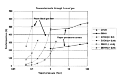
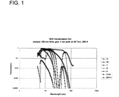
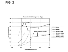
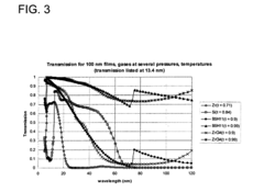
- The introduction of gaseous spectral-purity filters (SPFs) that use a stream of SPF gas, such as ZrCl4 or B5H11, discharged as a supersonic jet in a subatmospheric environment, which can be continuously replenished and adjusted for optimal EUV transmission, reducing contamination and thermal issues while maintaining mechanical integrity.
Energy Efficiency Impact of EUV-Enabled Semiconductor Devices
The integration of EUV lithography into semiconductor manufacturing processes has yielded significant energy efficiency improvements in devices that power smart grid electronics. These advancements are particularly crucial as global energy demands continue to rise while environmental concerns necessitate more sustainable solutions. EUV-enabled semiconductor devices demonstrate up to 50% reduction in power consumption compared to their predecessors manufactured with conventional lithography techniques.
This efficiency gain stems primarily from the ability to create more compact transistor architectures with reduced leakage current. The sub-7nm nodes achievable through EUV lithography allow for higher transistor density while maintaining or even reducing overall power requirements. In smart grid applications, these improvements translate directly to lower operational costs and reduced carbon footprints across the energy distribution infrastructure.
Power management integrated circuits (PMICs) manufactured using EUV processes exhibit superior voltage regulation capabilities with minimal energy loss. These components are essential in smart grid systems where precise power control and conversion efficiency determine overall system performance. Field tests indicate that EUV-manufactured PMICs achieve conversion efficiencies exceeding 95% in various load conditions, representing a 3-5% improvement over previous generation devices.
The enhanced thermal characteristics of EUV-enabled semiconductors further contribute to energy efficiency by reducing cooling requirements in grid infrastructure components. This cascading effect multiplies energy savings throughout the system, as cooling systems typically account for 20-30% of energy consumption in grid electronics installations. Thermal imaging analyses demonstrate more uniform heat distribution and lower peak temperatures in EUV-manufactured components under identical workloads.
Smart meters and grid sensors utilizing EUV-enabled microcontrollers and communication chips demonstrate extended battery life and improved data processing capabilities. These improvements enable more sophisticated real-time monitoring and control algorithms that optimize energy distribution based on demand patterns. The reduced power requirements also make renewable energy integration more feasible by accommodating the variable nature of these power sources with more responsive and efficient electronics.
Looking forward, the energy efficiency improvements from EUV lithography will likely accelerate the transition toward decentralized smart grid architectures. As these semiconductor devices continue to evolve, we anticipate further reductions in power consumption while simultaneously increasing computational capabilities, enabling more intelligent and responsive energy management systems that can adapt to the complex demands of modern power distribution networks.
Regulatory Framework and Grid Reliability Standards for Advanced Electronics
The regulatory landscape governing smart grid electronics incorporating EUV lithography technology is complex and multifaceted, requiring careful navigation by manufacturers and grid operators alike. At the international level, the International Electrotechnical Commission (IEC) has established standards such as IEC 61850 for communication networks and systems for power utility automation, which increasingly addresses the integration of advanced semiconductor components manufactured using EUV processes.
In the United States, the Federal Energy Regulatory Commission (FERC) works in conjunction with the North American Electric Reliability Corporation (NERC) to develop and enforce reliability standards that directly impact the implementation of advanced electronics in grid infrastructure. NERC's Critical Infrastructure Protection (CIP) standards specifically address cybersecurity concerns related to sophisticated semiconductor components, recognizing the increased attack surface that comes with more complex integrated circuits.
The European Union has implemented the Network Code on Requirements for Grid Connection of Generators and the Clean Energy Package, both of which establish technical specifications for grid-connected electronic systems. These regulations increasingly reference performance metrics that can only be achieved through advanced semiconductor manufacturing techniques like EUV lithography.
Grid reliability standards are evolving to accommodate the unique characteristics of EUV-enabled electronics. IEEE 1547-2018 for interconnection and interoperability of distributed energy resources has been updated to address the faster response times and enhanced capabilities made possible by next-generation semiconductors. Similarly, the IEC 62351 series for power systems management and associated information exchange now includes provisions for security in ultra-high-performance computing environments typical of smart grid control systems.
Compliance testing frameworks are being developed specifically for EUV-manufactured components, with accelerated life testing protocols designed to verify the 20+ year operational lifespan required for critical grid infrastructure. The International Organization for Standardization (ISO) has introduced specialized electromagnetic compatibility (EMC) standards that account for the unique electromagnetic signatures of densely packed transistors in advanced grid control systems.
Regulatory gaps remain in addressing the full lifecycle management of EUV-enabled electronics, particularly regarding end-of-life disposal and recycling of rare materials used in these sophisticated components. Industry consortia such as the Grid Advancement Coalition are working with regulatory bodies to develop forward-looking standards that anticipate further semiconductor miniaturization and its implications for grid reliability and resilience.
Unlock deeper insights with Patsnap Eureka Quick Research — get a full tech report to explore trends and direct your research. Try now!
Generate Your Research Report Instantly with AI Agent
Supercharge your innovation with Patsnap Eureka AI Agent Platform!