Comparison Between EUV Lithography and Traditional Photo Engraving Methods
OCT 14, 20259 MIN READ
Generate Your Research Report Instantly with AI Agent
Patsnap Eureka helps you evaluate technical feasibility & market potential.
EUV Lithography Evolution and Objectives
Extreme Ultraviolet (EUV) lithography represents a revolutionary advancement in semiconductor manufacturing technology, emerging from decades of research and development aimed at overcoming the physical limitations of traditional photolithography methods. The evolution of lithography technology has been driven by Moore's Law, which predicted the doubling of transistor density approximately every two years, necessitating increasingly precise fabrication techniques.
Traditional photolithography methods, which have dominated semiconductor manufacturing since the 1960s, utilize deep ultraviolet (DUV) light sources with wavelengths of 248nm and 193nm. These techniques have been progressively refined through innovations such as immersion lithography and multiple patterning. However, as feature sizes approached sub-10nm dimensions, the fundamental physical limitations of DUV wavelengths became insurmountable barriers to further miniaturization.
EUV lithography, operating at a significantly shorter wavelength of 13.5nm, emerged as the most promising solution to continue the semiconductor industry's scaling roadmap. The development of EUV technology began in the 1990s, but commercial viability remained elusive for decades due to formidable technical challenges including source power limitations, mask defectivity, and resist performance issues.
The primary objective of EUV lithography is to enable the continuation of Moore's Law by facilitating the production of increasingly smaller transistors with greater density and improved performance. Specifically, EUV aims to achieve reliable high-volume manufacturing of semiconductor devices at the 7nm node and beyond, while reducing the complexity and cost associated with multiple patterning techniques required by DUV lithography at these dimensions.
A secondary but equally important objective is to simplify the manufacturing process. Where DUV lithography at advanced nodes requires complex multi-patterning techniques that can involve 60-80 process steps for a single layer, EUV can potentially reduce this to 20-30 steps, significantly decreasing production time and cost while improving yield.
The technological trajectory of EUV lithography continues to evolve toward higher numerical aperture (High-NA) EUV systems, which promise to extend resolution capabilities even further. Current EUV systems operate at 0.33 NA, while next-generation High-NA EUV tools targeting 0.55 NA are under development to enable scaling to 3nm and below.
Understanding the evolution and objectives of EUV lithography provides essential context for comparing its capabilities, advantages, and limitations against traditional photolithography methods, particularly as the semiconductor industry navigates the increasing technical and economic challenges of continued scaling.
Semiconductor Industry Market Demands
The semiconductor industry has witnessed unprecedented growth in recent years, with the global market value reaching $555.9 billion in 2021 and projections indicating continued expansion to potentially exceed $1 trillion by 2030. This remarkable growth is primarily driven by increasing demands for advanced computing capabilities, artificial intelligence applications, and the proliferation of Internet of Things (IoT) devices across various sectors.
Central to this market expansion is the critical need for more sophisticated lithography technologies. As Moore's Law continues to guide industry development, manufacturers face mounting pressure to produce smaller, more efficient transistors on semiconductor wafers. The market demand for chips with sub-7nm process nodes has grown exponentially, with major players like TSMC, Samsung, and Intel racing to achieve 5nm, 3nm, and eventually 2nm process capabilities.
Consumer electronics represent the largest market segment driving lithography advancement, accounting for approximately 33% of semiconductor demand. Smartphones alone require billions of advanced chips annually, with each new generation demanding higher performance and lower power consumption that only cutting-edge lithography can deliver.
The automotive industry has emerged as another significant market driver, with modern vehicles incorporating up to 3,000 semiconductor chips. The transition toward electric and autonomous vehicles has intensified this demand, with projections suggesting a 15% annual growth rate in automotive semiconductor requirements through 2025.
Data centers and cloud computing infrastructure constitute a rapidly expanding market segment, with global spending on data center chips reaching $152 billion in 2021. These facilities require the most advanced processors possible to handle exponentially growing data processing needs, directly influencing lithography technology requirements.
The COVID-19 pandemic highlighted critical vulnerabilities in the semiconductor supply chain, resulting in unprecedented chip shortages across industries. This situation has accelerated governmental initiatives worldwide to establish domestic semiconductor manufacturing capabilities, with the US CHIPS Act allocating $52 billion and the European Chips Act committing €43 billion toward semiconductor industry development.
Market analysis reveals a clear bifurcation in lithography technology demands: high-volume manufacturers requiring extreme precision for cutting-edge applications versus those serving specialized markets with less stringent dimensional requirements. This dichotomy directly impacts the adoption rates of EUV versus traditional lithography methods, with market forecasts suggesting EUV equipment sales will grow at 24% CAGR through 2026, significantly outpacing traditional lithography equipment growth.
Current EUV Technology Challenges
Despite significant advancements in EUV lithography technology, several critical challenges continue to impede its widespread adoption and optimal performance. The most pressing issue remains the power source limitation. Current EUV systems operate with laser-produced plasma sources that generate 13.5nm wavelength light, but these sources struggle to achieve the power levels necessary for high-volume manufacturing. While the industry target is 250-300 watts, many deployed systems operate at lower power levels, resulting in reduced throughput and increased cost per wafer.
Mask defectivity presents another substantial challenge. EUV masks are fundamentally different from traditional photomasks, utilizing reflective rather than transmissive designs. The multilayer reflective coatings required for EUV wavelengths are susceptible to both surface and buried defects. Detection and repair of these defects remain technically difficult, with current inspection tools still evolving to meet the stringent requirements of sub-7nm node manufacturing.
Photoresist performance continues to be a limiting factor in EUV implementation. The photochemistry at EUV wavelengths differs significantly from traditional lithography, requiring novel resist materials. Current EUV resists face a persistent trade-off between sensitivity, resolution, and line-edge roughness—the so-called "triangle of death" in resist design. Improving one parameter typically degrades the others, creating a significant barrier to achieving optimal performance.
Stochastic effects have emerged as a fundamental challenge unique to EUV lithography. At the 13.5nm wavelength, the statistical variation in photon absorption becomes significant, leading to random variations in pattern formation. These stochastic effects manifest as line-edge roughness, line-width roughness, and in extreme cases, pattern failures such as bridging or broken lines. As feature sizes continue to shrink, these effects become increasingly problematic.
Infrastructure and supply chain limitations also constrain EUV adoption. The complex optical systems require ultra-precise mirrors with atomic-level smoothness, specialized vacuum systems, and highly purified gases. The supply chain for these components remains limited, with few vendors capable of meeting the exacting specifications required.
Cost remains perhaps the most significant barrier to widespread EUV adoption. EUV lithography tools represent the most expensive equipment in semiconductor manufacturing, with each system costing upwards of $150 million. When combined with higher operational costs due to lower throughput and increased maintenance requirements, the economic case for EUV implementation becomes challenging for all but the most advanced semiconductor manufacturers.
EUV vs Traditional Lithography Solutions
01 EUV Lithography Technology and Systems
Extreme Ultraviolet (EUV) lithography represents a significant advancement in semiconductor manufacturing, using short wavelength light (13.5nm) to create extremely fine circuit patterns. EUV systems typically include specialized light sources, reflective optics, and vacuum environments to overcome the challenges of working with this wavelength. These systems enable the production of smaller transistors and more densely packed integrated circuits compared to traditional lithography methods.- EUV Lithography Technology and Systems: Extreme Ultraviolet (EUV) lithography represents a significant advancement in semiconductor manufacturing, using short wavelength light (typically 13.5nm) to create extremely fine circuit patterns. EUV systems typically include specialized light sources, reflective optics, and vacuum environments to enable high-resolution patterning. This technology allows for the creation of smaller feature sizes than traditional optical lithography methods, supporting the continued miniaturization of semiconductor devices.
- Comparison Between EUV and Traditional Lithography Methods: Traditional photo engraving methods typically use longer wavelength light sources (193nm or 248nm) and refractive optics, while EUV lithography employs 13.5nm wavelength and reflective optics. Traditional methods often employ immersion techniques and multiple patterning to extend their resolution capabilities, whereas EUV offers inherently higher resolution but presents challenges in terms of source power, mask defects, and throughput. The transition from traditional to EUV lithography represents a significant shift in semiconductor manufacturing technology.
- Photomask and Reticle Technology for Advanced Lithography: Photomasks and reticles are critical components in both EUV and traditional lithography processes. For EUV, reflective masks with multilayer coatings are used instead of the transmissive masks employed in traditional lithography. The design, fabrication, and inspection of these masks present unique challenges, including defect detection and repair at nanometer scales. Advanced computational techniques are often employed to optimize mask designs for specific lithography processes, enhancing pattern fidelity and process windows.
- Resist Materials and Process Chemistry: Specialized photoresist materials have been developed for both EUV and traditional lithography processes. EUV resists must be highly sensitive due to the limited source power available, while maintaining high resolution and low line edge roughness. Chemical amplification mechanisms, metal-containing resists, and novel development processes are employed to meet these requirements. The interaction between resist chemistry and exposure conditions significantly impacts the final pattern quality and manufacturing yield.
- Integration and Manufacturing Considerations: Implementing EUV lithography in production environments requires significant modifications to manufacturing workflows compared to traditional methods. Considerations include vacuum handling systems, contamination control, and integration with existing process steps. Economic factors such as tool cost, throughput, and yield also play important roles in the adoption of EUV technology. Hybrid approaches that combine EUV and traditional lithography techniques are often employed to optimize cost and performance for different layers of semiconductor devices.
02 Comparison Between EUV and Traditional Photolithography
Traditional photolithography methods use longer wavelengths (193nm or 248nm) and transmission-based optical systems, while EUV lithography employs 13.5nm wavelength and reflection-based systems. Traditional methods often require multiple patterning steps to achieve what EUV can do in a single exposure. However, traditional methods benefit from decades of optimization and lower implementation costs, while EUV systems face challenges related to power requirements, mask defects, and throughput limitations.Expand Specific Solutions03 Mask Technology and Defect Management
EUV masks differ significantly from traditional photomasks, requiring reflective rather than transmissive designs. They consist of multiple layers of materials that reflect EUV radiation in specific patterns. Defect management is particularly critical in EUV lithography due to the shorter wavelength making even tiny imperfections significant. Advanced inspection and repair technologies are employed to identify and address defects in both the mask substrate and the reflective multilayer structure.Expand Specific Solutions04 Resist Materials and Processing
Photoresist materials for EUV lithography require different chemical compositions compared to those used in traditional photolithography. EUV resists must be highly sensitive to the 13.5nm wavelength while maintaining resolution, line edge roughness, and pattern fidelity requirements. The development process also differs, with EUV often requiring specialized post-exposure bake conditions and development chemicals to achieve optimal results. Research continues to improve resist sensitivity and reduce pattern collapse issues.Expand Specific Solutions05 Integration and Manufacturing Challenges
Implementing EUV lithography in production environments presents significant challenges including high vacuum requirements, contamination control, and thermal management. The integration of EUV with existing semiconductor manufacturing processes requires careful optimization of workflow and equipment. While traditional photolithography methods benefit from established infrastructure and processes, EUV adoption necessitates substantial investment in new equipment, facilities, and training. The industry continues to address challenges related to cost, throughput, and reliability.Expand Specific Solutions
Leading Semiconductor Equipment Manufacturers
EUV lithography represents a significant technological advancement in semiconductor manufacturing, currently in the growth phase with a market expected to reach $10 billion by 2025. The technology has matured rapidly, with ASML holding the dominant position as the sole supplier of EUV lithography systems. Key players like Taiwan Semiconductor Manufacturing Co., Samsung Electronics, and Intel are leading adopters, while Applied Materials, Lam Research, and Carl Zeiss SMT provide critical supporting technologies. Traditional photoengraving methods remain relevant for less advanced nodes, with companies like Nikon and Canon maintaining market share in this segment. The competitive landscape shows a clear technological stratification, with only the most advanced manufacturers able to implement EUV technology due to its complexity and cost.
Taiwan Semiconductor Manufacturing Co., Ltd.
Technical Solution: TSMC has pioneered the implementation of EUV lithography in high-volume manufacturing, being the first to deploy ASML's EUV systems at scale for commercial chip production. Their approach integrates EUV with traditional lithography in a hybrid model that optimizes cost and performance. For critical layers requiring the highest resolution, TSMC employs EUV single-pattern techniques, while using traditional 193nm immersion lithography with multi-patterning for less demanding layers[3]. TSMC's 5nm process technology (N5) represents their first node with extensive EUV implementation, using up to 14 EUV layers compared to only 4-5 EUV layers in their 7nm process. This strategic deployment has enabled a 1.84x logic density improvement and 15% performance gain over their previous node[4]. TSMC has developed proprietary resist materials and process recipes specifically optimized for EUV implementation, addressing challenges like stochastic effects and pattern roughness. Their EUV integration strategy includes specialized metrology systems for defect inspection and advanced computational lithography techniques to maximize the technology's capabilities while managing the economic considerations of deploying such expensive equipment.
Strengths: Industry-leading implementation of EUV in high-volume manufacturing; optimized hybrid approach balancing EUV and traditional lithography; demonstrated ability to scale to 3nm and beyond with EUV; superior yield management. Weaknesses: Extremely high capital expenditure requirements; dependency on ASML as sole EUV equipment supplier; challenges in managing EUV-specific defects and process variations at scale.
Samsung Electronics Co., Ltd.
Technical Solution: Samsung has developed a comprehensive EUV implementation strategy that competes directly with TSMC in advanced semiconductor manufacturing. Their approach focuses on maximizing the benefits of EUV while addressing its economic challenges through process optimization. Samsung's 7nm LPP (Low Power Plus) process was their first to incorporate EUV lithography, reducing mask layers by 20% compared to traditional multi-patterning techniques[5]. For their 5nm process, Samsung expanded EUV usage to approximately 12-14 critical layers, enabling a 25% logic area reduction compared to their 7nm process. Samsung has invested heavily in developing specialized EUV infrastructure, including dedicated clean rooms with enhanced vibration control, temperature stability to within 0.1°C, and specialized reticle handling systems to prevent contamination[6]. Their EUV implementation includes proprietary computational lithography techniques that optimize mask designs specifically for EUV's unique optical characteristics. Samsung has also pioneered the development of specialized photoresists with higher sensitivity for EUV exposure, helping to address throughput limitations while maintaining pattern fidelity. Their roadmap includes expanding EUV usage in memory manufacturing, particularly for DRAM, where they've demonstrated EUV-based patterning for sub-14nm DRAM production.
Strengths: Comprehensive EUV implementation across logic and memory products; significant process simplification compared to multi-patterning; demonstrated ability to scale to 3nm with EUV; vertical integration advantages in materials and equipment. Weaknesses: High capital expenditure requirements; challenges in EUV source power stability affecting throughput; complex facility requirements; dependency on ASML for EUV equipment.
Key Patents in EUV Technology
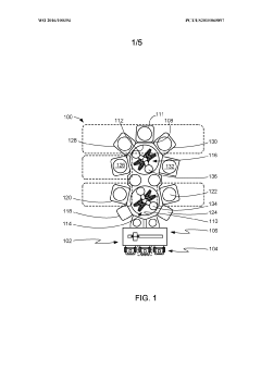
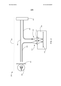
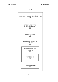
Monitoring system for deposition and method of operation thereof
PatentWO2016100394A1
Innovation
- A monitoring and deposition control system that includes a deposition chamber, a sensor array for in-situ broadband reflectometry to monitor layer thickness changes, and a processing unit to adjust deposition parameters in real-time, ensuring precise control of Mo/Si multilayer stacks for EUV mask blanks.
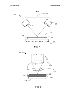
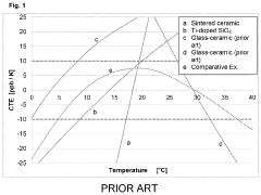
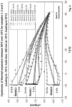
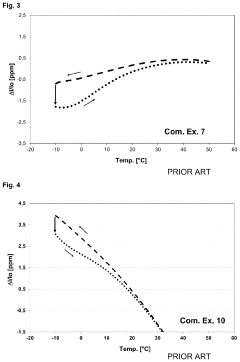
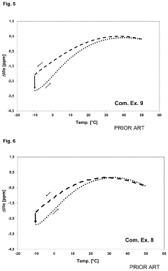
EUVL precision component with specific thermal expansion behavior
PatentPendingUS20240077798A1
Innovation
- A precision EUVL component with an average CTE of at most 0±0.1×10⁻⁶/K and thermal hysteresis of <0.1 ppm in the temperature range from 19 to 25°C, utilizing an LAS glass-ceramic composition with optimized SiO2, Li2O, and nucleating agents like TiO2, ZrO2, and WO3, which minimizes thermal hysteresis and ensures zero expansion.
Economic Impact Analysis
The economic implications of transitioning from traditional photolithography to Extreme Ultraviolet (EUV) lithography represent a significant shift in semiconductor manufacturing economics. Initial capital expenditure for EUV technology is substantially higher, with each EUV lithography machine costing approximately $150-200 million compared to $30-40 million for advanced DUV (Deep Ultraviolet) systems. This steep investment creates a considerable barrier to entry, limiting EUV adoption primarily to industry giants like TSMC, Samsung, and Intel.
However, the long-term economic benefits of EUV technology are becoming increasingly apparent. Process simplification represents one of the most significant advantages, as EUV can replace multiple DUV exposure steps with a single exposure. For advanced nodes below 7nm, traditional multi-patterning approaches may require 4-5 exposure steps for a single layer, whereas EUV can accomplish the same result in one step. This reduction translates to approximately 20-30% lower overall production costs for high-volume manufacturing once the initial investment is amortized.
The economic impact extends to operational efficiency as well. EUV lithography reduces cycle time by eliminating multiple processing steps, potentially increasing throughput by 15-25% for critical layers. Additionally, the improved resolution and pattern fidelity of EUV reduces defect rates and increases yield, particularly for the most complex chip designs. Industry reports suggest yield improvements of 3-8% for leading-edge nodes when transitioning from multi-patterning DUV to EUV, representing significant cost savings in high-volume production environments.
From a market perspective, EUV technology has created new economic hierarchies within the semiconductor ecosystem. ASML's effective monopoly on EUV equipment manufacturing has positioned the company as a critical gatekeeper in advanced semiconductor production. This concentration of technological capability has geopolitical implications, with nations increasingly viewing access to EUV technology as a matter of economic security and technological sovereignty.
The broader economic impact on the semiconductor value chain is equally profound. Chip designers can now implement more complex architectures that were previously impractical due to manufacturing limitations. This capability expansion drives innovation in end products across computing, telecommunications, automotive, and consumer electronics sectors, potentially generating trillions in economic value over the next decade.
Despite these advantages, the economic case for EUV adoption remains nuanced and depends heavily on production volume, chip complexity, and target market. For high-volume, leading-edge applications, the economic benefits clearly favor EUV. For specialty chips and lower-volume production, traditional lithography methods often remain more economically viable, creating a bifurcated market where both technologies will coexist for the foreseeable future.
Environmental Considerations in Lithography
Environmental considerations have become increasingly critical in semiconductor manufacturing processes, particularly in lithography technologies. Traditional photolithography methods typically employ deep ultraviolet (DUV) light sources that operate at wavelengths of 248nm or 193nm, requiring complex chemical processes with significant environmental implications. These conventional approaches utilize substantial quantities of photoresist chemicals, developers, and cleaning solvents that contain volatile organic compounds (VOCs), perfluorinated compounds (PFCs), and other potentially hazardous materials.
EUV lithography, while offering superior resolution capabilities, presents a different environmental profile. The technology operates at an extremely short wavelength of 13.5nm, requiring less photoresist material per wafer. This reduction in chemical usage represents a potential environmental advantage. However, EUV systems demand significantly higher energy consumption—approximately 10-15 times more power than traditional DUV systems—primarily due to the complex plasma generation process required to produce EUV radiation.
Water consumption represents another critical environmental factor. Traditional lithography methods typically require 5,000-10,000 liters of ultra-pure water per wafer for rinsing and cleaning processes. EUV systems have demonstrated potential for reduced water usage through more efficient process designs, though the overall manufacturing ecosystem still demands substantial water resources.
Greenhouse gas emissions differ significantly between these technologies. Traditional photolithography processes emit considerable amounts of perfluorocompounds (PFCs) with high global warming potential. EUV systems produce fewer direct process emissions but their elevated energy requirements translate to higher indirect carbon emissions in regions dependent on fossil fuel energy generation.
Waste management challenges also vary between these approaches. Traditional methods generate substantial liquid waste streams containing photoresist residues, developers, and cleaning agents requiring specialized treatment. EUV processes produce less chemical waste but generate more complex maintenance-related waste, including specialized mirrors and components containing rare earth elements that present recycling challenges.
Regulatory frameworks worldwide are evolving to address these environmental concerns. The European Union's Restriction of Hazardous Substances (RoHS) directive and various global initiatives to reduce perfluorinated chemicals are increasingly influencing lithography technology development. Leading semiconductor manufacturers have established ambitious sustainability targets, driving innovation in both traditional and EUV lithography to minimize environmental footprints while maintaining technological advancement.
Unlock deeper insights with Patsnap Eureka Quick Research — get a full tech report to explore trends and direct your research. Try now!
Generate Your Research Report Instantly with AI Agent
Supercharge your innovation with Patsnap Eureka AI Agent Platform!