

New Advances in EUV Lithography for Compact Device Technologies
OCT 14, 20259 MIN READ
Generate Your Research Report Instantly with AI Agent
PatSnap Eureka helps you evaluate technical feasibility & market potential.
EUV Lithography Evolution and Objectives
Extreme Ultraviolet (EUV) lithography represents a revolutionary advancement in semiconductor manufacturing technology, marking a significant departure from traditional deep ultraviolet (DUV) lithography methods. The evolution of EUV technology spans over three decades, beginning in the 1980s with initial research into short-wavelength lithography techniques. By utilizing 13.5nm wavelength light, EUV lithography enables the creation of significantly smaller features compared to the 193nm wavelength used in DUV systems, facilitating the continued miniaturization of semiconductor devices in accordance with Moore's Law.
The development trajectory of EUV lithography has been characterized by persistent efforts to overcome substantial technical challenges. Early research focused primarily on light source development, with significant breakthroughs occurring in the early 2000s through the implementation of laser-produced plasma (LPP) technology. This innovation, coupled with advancements in multilayer mirror optics and resist chemistry, has gradually transformed EUV from an experimental concept into a commercially viable manufacturing technology.
Industry adoption has accelerated markedly since 2019, when leading semiconductor manufacturers began incorporating EUV lithography into high-volume production processes. This transition represents the culmination of collaborative efforts across the semiconductor ecosystem, including equipment manufacturers, material suppliers, and chip designers, all working to integrate this complex technology into production environments.
The primary objective of current EUV lithography development is to enable the fabrication of increasingly compact and powerful semiconductor devices while maintaining economic viability. Specifically, the technology aims to support node transitions below 7nm, with particular emphasis on 5nm, 3nm, and eventually 2nm process nodes. These advancements are critical for meeting the growing computational demands of artificial intelligence, high-performance computing, and next-generation mobile devices.
Secondary objectives include improving system throughput to enhance manufacturing efficiency, reducing defect rates to increase yield, and developing more sensitive photoresist materials to optimize exposure performance. Additionally, significant research is being directed toward extending EUV capabilities through high-numerical-aperture (high-NA) systems, which promise to further reduce feature sizes and extend the technology's roadmap well into the next decade.
The evolution of EUV lithography continues to be driven by the semiconductor industry's relentless pursuit of greater integration density and improved device performance. As the technology matures, it is expected to enable new device architectures, including three-dimensional structures and novel materials integration, further expanding the capabilities of modern electronic systems while addressing increasing concerns about power efficiency and thermal management.
Semiconductor Industry Demand Analysis
The semiconductor industry is experiencing unprecedented demand for advanced lithography solutions, particularly EUV (Extreme Ultraviolet) lithography, driven by the relentless pursuit of Moore's Law and the need for increasingly compact device technologies. Market analysis indicates that the global semiconductor equipment market is projected to reach $120 billion by 2025, with lithography equipment accounting for approximately 30% of this value.
The demand for EUV lithography is primarily fueled by the production of advanced logic nodes (5nm and below) and high-density memory chips. Major semiconductor manufacturers including TSMC, Samsung, and Intel have committed substantial investments in EUV technology, with TSMC alone allocating over $15 billion for EUV equipment in their latest capacity expansion plans.
Consumer electronics continue to be the largest end-user segment driving demand for advanced semiconductors, with smartphones, tablets, and wearable devices requiring increasingly powerful yet energy-efficient chips. The automotive sector represents the fastest-growing segment, with compound annual growth rates exceeding 15% as vehicles incorporate more advanced driver assistance systems and autonomous driving capabilities.
Market research indicates that the transition to EUV lithography is accelerating, with the number of EUV layers in leading-edge chips increasing from 5-10 layers in 7nm nodes to 20-30 layers in 3nm nodes. This transition is creating significant demand for not only EUV lithography systems but also complementary technologies including photoresists, pellicles, and inspection tools.
Regional analysis shows Asia-Pacific dominating the market with over 65% share, led by Taiwan, South Korea, and increasingly China. North America and Europe follow with significant investments in both manufacturing and research facilities. The concentration of advanced semiconductor manufacturing in specific geographic regions has heightened concerns about supply chain resilience, further stimulating investments in domestic semiconductor capabilities across multiple regions.
The industry faces several demand-side challenges, including the high capital costs associated with EUV implementation (with each EUV lithography system costing approximately $150 million), skilled workforce shortages, and geopolitical tensions affecting technology access. Despite these challenges, market forecasts predict EUV lithography equipment demand will grow at 15-20% annually through 2028.
Long-term market trends indicate that emerging applications in quantum computing, artificial intelligence, and 6G communications will further drive demand for advanced lithography solutions beyond current projections, potentially creating new market segments for specialized semiconductor devices manufactured using customized EUV processes.
EUV Technical Challenges and Global Development Status
Extreme Ultraviolet (EUV) lithography represents a revolutionary advancement in semiconductor manufacturing, yet faces significant technical challenges that have influenced its global development trajectory. The primary technical hurdle remains the EUV light source, which requires generating and maintaining stable 13.5nm wavelength radiation. Current systems utilize laser-produced plasma from tin droplets, achieving power levels of 250-300W, though industry roadmaps demand 500W+ for high-volume manufacturing efficiency.
Photomask defectivity presents another critical challenge. EUV masks utilize complex multilayer reflective structures rather than traditional transmissive designs, making defect detection and repair substantially more difficult. The absence of pellicles in early EUV systems exacerbated contamination risks, though recent advancements in pellicle technology have improved but not eliminated this concern.
Photoresist performance continues to challenge manufacturers, with the fundamental trade-off between sensitivity, resolution, and line-edge roughness (the "triangle of death") remaining unresolved. Current EUV resists struggle to simultaneously achieve high sensitivity for throughput while maintaining the resolution and pattern fidelity required for advanced nodes.
Geographically, EUV technology development demonstrates clear concentration patterns. The Netherlands dominates equipment manufacturing through ASML's monopoly on EUV scanners. Japan leads in mask blanks and inspection tools, with companies like Lasertec controlling critical segments of the ecosystem. The United States maintains leadership in light source technology and computational lithography, while South Korea and Taiwan have become centers for implementation expertise.
China's participation in EUV development remains limited due to export restrictions, creating a significant technological divide in the global semiconductor landscape. This geopolitical dimension has accelerated alternative lithography research in regions with restricted EUV access.
Recent technical progress has focused on high-NA (numerical aperture) EUV systems, promising resolution improvements from 13nm to 8nm. However, these systems introduce new challenges in mask making, stage design, and computational requirements. Stochastic effects—random variations at atomic scales—have emerged as fundamental physics limitations requiring novel mitigation strategies combining materials science and computational approaches.
The EUV ecosystem has evolved toward greater vertical integration, with key players securing supply chains through strategic investments and acquisitions, reflecting both the technology's strategic importance and the specialized expertise required across the value chain.
Current EUV Implementation Strategies
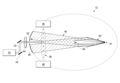
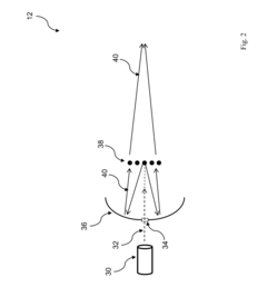
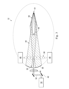
01 Compact EUV source designs
Compact designs for EUV light sources focus on reducing the overall footprint while maintaining performance. These innovations include optimized plasma generation chambers, integrated cooling systems, and efficient collector optics arrangements. The compact designs enable easier integration into lithography systems while addressing space constraints in semiconductor manufacturing facilities.- Compact EUV source and illumination systems: Compact extreme ultraviolet (EUV) light source designs and illumination systems that reduce the overall footprint of lithography equipment. These innovations include optimized source architectures, efficient collector optics, and integrated illumination systems that maintain high output power while minimizing space requirements. Such compact designs enable more efficient cleanroom utilization while maintaining the necessary performance for advanced semiconductor manufacturing.
- Miniaturized optical components for EUV lithography: Development of miniaturized optical components specifically designed for EUV lithography systems to reduce overall system size. These components include compact mirrors, reduced-size projection optics, and space-efficient beam delivery systems. Advanced manufacturing techniques enable the creation of smaller yet highly precise optical elements that maintain the stringent requirements for EUV wavelength while contributing to overall system compactness.
- Integrated cooling and vacuum systems for compact EUV tools: Innovative approaches to integrate cooling and vacuum systems in EUV lithography equipment to minimize space requirements. These designs incorporate efficient thermal management solutions, compact vacuum pumping arrangements, and optimized component layouts that reduce the overall footprint while maintaining the necessary environmental conditions for EUV operation. The integration of these critical subsystems contributes significantly to achieving more compact lithography tools.
- Modular and stackable EUV lithography system designs: Modular and stackable system architectures that enable more compact EUV lithography equipment. These designs feature vertically integrated components, reconfigurable modules, and optimized spatial arrangements that maximize functionality while minimizing floor space requirements. The modular approach also facilitates easier maintenance and upgrades without requiring complete system replacement, contributing to both compactness and operational efficiency.
- Compact EUV wafer handling and positioning systems: Space-efficient wafer handling and positioning systems specifically designed for compact EUV lithography tools. These innovations include miniaturized stage mechanisms, integrated wafer transport systems, and optimized alignment components that maintain nanometer-level precision while requiring less space. Advanced control systems enable precise positioning in a reduced form factor, contributing to the overall compactness of EUV lithography equipment.
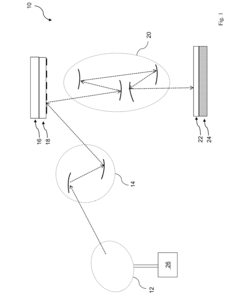
02 Optical system miniaturization
Miniaturization of optical components in EUV lithography systems contributes significantly to overall compactness. This includes innovative designs for mirrors, lenses, and beam delivery systems that maintain optical performance while reducing size. Advanced materials and manufacturing techniques enable the creation of smaller optical elements that can withstand the intense conditions of EUV lithography.Expand Specific Solutions03 Integrated cooling and thermal management
Compact thermal management solutions are critical for EUV lithography systems due to the high heat loads generated. These innovations include integrated cooling channels, advanced heat dissipation materials, and optimized thermal interfaces. Efficient thermal management in a reduced footprint helps maintain system stability and component longevity while contributing to overall system compactness.Expand Specific Solutions04 Compact vacuum and environmental control systems
EUV lithography requires sophisticated vacuum systems that have been redesigned for compactness. These systems incorporate miniaturized pumps, integrated vacuum chambers, and efficient sealing technologies. Compact environmental control systems maintain the necessary conditions for EUV lithography while occupying minimal space within the overall system architecture.Expand Specific Solutions05 Modular and stackable system architectures
Modular approaches to EUV lithography system design enable more compact overall configurations. These architectures feature stackable components, standardized interfaces, and reconfigurable layouts that optimize space utilization. The modular design philosophy allows for easier maintenance access and system upgrades while maintaining a compact footprint in semiconductor fabrication facilities.Expand Specific Solutions
Leading EUV Equipment Manufacturers and Chip Producers
EUV lithography technology for compact device manufacturing is currently in the growth phase, with the market expected to reach $10 billion by 2025. The competitive landscape is dominated by ASML Netherlands BV, which holds a near-monopoly on EUV lithography equipment production. Leading semiconductor manufacturers like Taiwan Semiconductor Manufacturing Co., Samsung Electronics, and Intel are driving adoption, investing heavily in EUV technology to enable sub-7nm node production. The technology maturity varies significantly across players, with TSMC and Samsung at the forefront of implementation, while companies like SMIC and Shanghai Sinyang Semiconductor Materials are working to close the technological gap. Supporting ecosystem players including Carl Zeiss SMT (optical systems), Applied Materials, and Lam Research (process tools) are critical to the technology's advancement and integration into manufacturing workflows.
Taiwan Semiconductor Manufacturing Co., Ltd.
Technical Solution: TSMC has pioneered advanced EUV lithography implementation in high-volume manufacturing, particularly for their 5nm and 3nm process nodes. Their approach involves multi-patterning EUV techniques that enable critical dimension control below 20nm. TSMC has developed specialized pellicles that increase EUV transmission rates to over 88%, significantly improving throughput and yield. Their EUV implementation includes custom photoresist materials optimized for sensitivity and line edge roughness reduction. TSMC has also created an integrated computational lithography platform that combines machine learning algorithms with optical proximity correction to enhance pattern fidelity. Their latest innovation includes stochastic defect mitigation strategies that have reduced random defects by approximately 65% compared to earlier EUV implementations, enabling higher yields for their most advanced nodes.
Strengths: Industry-leading EUV implementation with proven high-volume manufacturing capability; superior defect control and yield management; advanced computational lithography integration. Weaknesses: Extremely high capital costs for EUV equipment and facility requirements; technology heavily dependent on ASML as the sole EUV scanner supplier.
Samsung Electronics Co., Ltd.
Technical Solution: Samsung has developed a comprehensive EUV lithography strategy centered on their DRAM and logic fabrication processes. Their approach includes custom-designed EUV masks with advanced absorber materials that improve contrast by approximately 30% compared to conventional masks. Samsung has pioneered the use of dry EUV resist technology that reduces pattern collapse issues while maintaining sensitivity at acceptable levels for high-volume manufacturing. Their multi-layer resist strategy enables aspect ratios suitable for advanced 3D structures in memory devices. Samsung has also implemented specialized metrology systems for in-line monitoring of EUV-specific defects, with automated classification algorithms that have improved defect detection rates by over 40%. Their EUV implementation includes customized dose control mechanisms that compensate for mask heating effects, maintaining critical dimension uniformity across the wafer.
Strengths: Successful integration of EUV into both memory and logic production; innovative resist and mask technologies; strong vertical integration with Samsung's equipment division. Weaknesses: Higher operational costs compared to traditional lithography; challenges with EUV source reliability and uptime in early implementations.
Breakthrough Patents in EUV Resolution Enhancement
Collector in an Extreme Ultraviolet Lithography System with Optimal Air Curtain Protection
PatentActiveUS20160306282A1
Innovation
- An EUV radiation source with a collector module integrated gas supply mechanism forms an air curtain using hydrogen gas, creating a protective layer on the collector surface and a purge cone to prevent contamination, utilizing a supply gap and gas pipeline with inward and outward entrances to ensure comprehensive coverage.
Extreme ultraviolet radiation imaging
PatentInactiveUS20050243390A1
Innovation
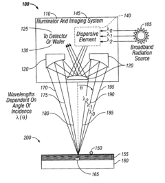
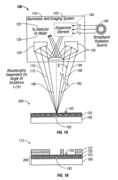
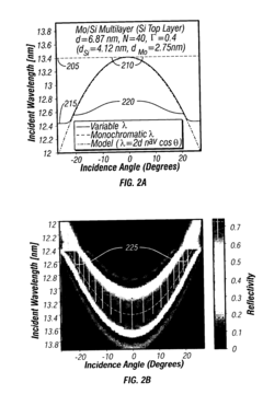
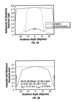
- Modulating the radiation wavelength and incident angle on reflective masks and mirrors in EUVL systems to increase the usable numerical aperture and resolution, utilizing a spectrally dispersive optical element and graded multi-layer coatings to enhance reflectivity across a range of angles and wavelengths.
Supply Chain Resilience for EUV Materials
The EUV lithography supply chain represents a complex global network with significant vulnerabilities that require strategic management. Critical materials for EUV processes, including specialized photoresists, pellicles, and mask blanks, often originate from limited geographical sources, creating potential bottlenecks. The COVID-19 pandemic exposed these vulnerabilities when manufacturing disruptions in Asia impacted the entire semiconductor industry, causing delays in advanced node production.
Leading semiconductor manufacturers have responded by implementing multi-sourcing strategies for key EUV materials. ASML, the sole provider of EUV lithography equipment, has established partnerships with multiple suppliers across different regions to ensure continuity of critical components. Intel and Samsung have invested in domestic supply chain development, creating regional manufacturing clusters to reduce dependency on cross-border logistics.
Material qualification represents another significant challenge in supply chain resilience. The extreme precision required for EUV processes means that alternative suppliers must meet stringent specifications, often requiring 12-18 months of validation before implementation. This timeline creates inherent rigidity in the supply chain that cannot be quickly reconfigured during disruptions.
Stockpiling has emerged as a common mitigation strategy, with major foundries maintaining 3-6 month reserves of critical EUV materials. However, this approach ties up significant capital and creates storage challenges for photosensitive materials with limited shelf life. Advanced inventory management systems using AI forecasting have been deployed to optimize these reserves.
Geopolitical tensions have further complicated EUV material supply chains. Export controls and technology restrictions between major semiconductor-producing nations have created additional compliance requirements and uncertainty. Industry consortia like SEMI have established working groups focused specifically on developing standards and contingency plans for EUV material supply chains.
Looking forward, vertical integration is becoming more prevalent as companies seek greater control over their supply chains. TSMC has invested in joint ventures with key material suppliers, while Samsung has expanded its internal capabilities for certain EUV-specific chemicals. These approaches help insulate companies from external disruptions but require substantial capital investment and technical expertise.
The industry is also exploring material innovations that could reduce supply chain vulnerabilities. Research into alternative photoresist chemistries that utilize more readily available compounds could decrease dependency on rare elements, while advances in recycling technologies for expensive materials like ruthenium are showing promise for reducing overall material requirements.
Environmental Impact of EUV Manufacturing Processes
The environmental impact of EUV lithography manufacturing processes represents a critical consideration as this advanced technology becomes more widely adopted in semiconductor fabrication. EUV systems consume substantial energy, with a single EUV lithography machine requiring approximately 1 MW of power during operation—significantly higher than traditional DUV lithography tools. This increased energy demand stems primarily from the complex laser-produced plasma process needed to generate EUV light at 13.5nm wavelength.
Water usage presents another significant environmental concern. EUV systems require ultra-pure water for cooling and cleaning processes, with consumption rates estimated at 5,000-10,000 gallons per day per tool. This places considerable strain on local water resources, particularly in semiconductor manufacturing hubs already facing water scarcity challenges.
Chemical consumption and waste generation also contribute to EUV's environmental footprint. The process utilizes various chemicals including photoresists, developers, and cleaning agents, many containing perfluorinated compounds (PFCs) with high global warming potential. Additionally, tin debris management systems generate waste streams requiring specialized disposal protocols to prevent environmental contamination.
Greenhouse gas emissions associated with EUV manufacturing extend beyond direct energy consumption. The production of specialized gases like hydrogen for the EUV source and the manufacturing of complex optical components involve carbon-intensive processes. Industry analyses suggest the carbon footprint of establishing an EUV manufacturing line is 30-40% higher than comparable DUV facilities.
Recent advancements have begun addressing these environmental challenges. Leading equipment manufacturers have implemented energy recovery systems that capture and reuse waste heat, reducing net energy consumption by up to 20%. Water recycling technologies have also improved, with closed-loop systems now capable of reclaiming up to 85% of process water.
The semiconductor industry has initiated collaborative efforts to develop more environmentally sustainable EUV processes. The "Green Lithography Consortium" established in 2022 brings together equipment manufacturers, chemical suppliers, and chip producers to set environmental benchmarks and develop next-generation eco-friendly materials specifically for EUV applications. These initiatives aim to reduce the environmental impact while maintaining the technological advantages that EUV lithography provides for compact device technologies.
Unlock deeper insights with PatSnap Eureka Quick Research — get a full tech report to explore trends and direct your research. Try now!
Generate Your Research Report Instantly with AI Agent
Supercharge your innovation with PatSnap Eureka AI Agent Platform!