EUV Lithography: The Central Force in Moore's Law Perspectives
OCT 14, 20259 MIN READ
Generate Your Research Report Instantly with AI Agent
Patsnap Eureka helps you evaluate technical feasibility & market potential.
EUV Lithography Evolution and Objectives
Extreme Ultraviolet (EUV) lithography represents a revolutionary advancement in semiconductor manufacturing technology, marking a significant milestone in the continued pursuit of Moore's Law. The evolution of lithography technology has been characterized by a progressive reduction in wavelength, from mercury lamps (436nm, 405nm, 365nm) to excimer lasers (248nm KrF, 193nm ArF), and finally to EUV at 13.5nm. This dramatic wavelength reduction enables the creation of significantly smaller circuit features, essential for advancing semiconductor node technology.
The development of EUV lithography spans over three decades, beginning in the 1980s with initial research into extreme ultraviolet light sources. The 1990s saw the formation of crucial industry consortia like EUV LLC, which brought together major semiconductor manufacturers to address the immense technical challenges. By the early 2000s, prototype EUV systems were demonstrating feasibility, though numerous obstacles remained in source power, mask technology, and resist chemistry.
A critical turning point occurred in 2016-2017 when ASML delivered the first production-ready EUV systems, the NXL:3400B, capable of meeting commercial requirements. This achievement represented the culmination of over $15 billion in research and development investment across the industry, highlighting the extraordinary technical complexity and economic significance of EUV technology.
The primary objective of EUV lithography development has been to enable semiconductor scaling beyond the physical limitations of traditional optical lithography. Specifically, EUV aims to facilitate high-volume manufacturing of integrated circuits at the 7nm node and beyond, where conventional 193nm immersion lithography becomes economically impractical due to multi-patterning requirements. EUV technology reduces process complexity by allowing single-exposure patterning for critical layers, improving yield and reducing manufacturing costs at advanced nodes.
Looking forward, the EUV technology roadmap includes several key objectives: increasing source power to improve throughput, enhancing resolution through high numerical aperture (High-NA) systems, developing more sensitive photoresists, and improving mask infrastructure. ASML's High-NA EUV systems, with a numerical aperture of 0.55 compared to current 0.33 systems, aim to extend EUV lithography to the 2nm node and potentially beyond, supporting Moore's Law well into the 2030s.
The successful implementation of EUV lithography has profound implications for the semiconductor industry's ability to maintain technological advancement rates, supporting innovations in artificial intelligence, quantum computing, and other emerging technologies that depend on continued transistor density improvements.
Semiconductor Industry Demand Analysis
The semiconductor industry's demand for advanced lithography technologies, particularly EUV (Extreme Ultraviolet) lithography, has been driven by the relentless pursuit of Moore's Law and the economic benefits of continued miniaturization. Market analysis indicates that the global semiconductor industry, valued at approximately $573 billion in 2022, is projected to reach $1.38 trillion by 2030, with a compound annual growth rate of 12.28%.
EUV lithography represents a critical enabling technology for this growth trajectory, as traditional DUV (Deep Ultraviolet) lithography has reached its physical limits for advanced node production. The market demand for EUV lithography systems has shown remarkable resilience despite their high cost, with each system priced between $150-200 million. This resilience stems from the technology's ability to reduce multi-patterning steps, thereby improving yield and lowering overall production costs for advanced nodes below 7nm.
Industry analysis reveals that leading semiconductor manufacturers have committed substantial capital expenditure toward EUV implementation. TSMC, Samsung, and Intel collectively planned to invest over $200 billion in capacity expansion between 2021 and 2023, with a significant portion allocated to EUV-based production lines. This investment surge reflects the strategic importance of EUV technology in maintaining competitive advantage in the high-performance computing, mobile, automotive, and AI chip markets.
The demand for EUV lithography is further amplified by emerging applications in artificial intelligence, 5G/6G telecommunications, autonomous vehicles, and high-performance computing. These applications require increasingly powerful and energy-efficient chips that can only be manufactured using the most advanced process nodes enabled by EUV technology. Market forecasts suggest that by 2025, over 70% of leading-edge logic chips will be manufactured using EUV lithography.
Regional analysis indicates shifting dynamics in the semiconductor manufacturing landscape, with significant investments in domestic chip production capabilities across the United States, Europe, Japan, South Korea, and China. This regionalization trend, driven by supply chain security concerns and national technology policies, is creating new demand centers for advanced lithography equipment, including EUV systems.
The economic value proposition of EUV lithography remains compelling despite its high initial investment costs. Industry data shows that the cost-per-transistor continues to decrease with each node advancement enabled by EUV, maintaining the economic viability of Moore's Law. This cost efficiency, coupled with performance improvements, continues to drive demand from both established semiconductor manufacturers and emerging foundries seeking to compete in advanced node production.
EUV Technology Status and Barriers
Extreme Ultraviolet (EUV) lithography represents a revolutionary advancement in semiconductor manufacturing, currently deployed in leading-edge production nodes below 7nm. The technology utilizes 13.5nm wavelength light to achieve unprecedented resolution in chip fabrication. Despite its commercial implementation by industry leaders like TSMC, Samsung, and Intel, EUV technology faces significant technical barriers that constrain its full potential.
The primary challenge remains the EUV light source efficiency. Current systems operate at approximately 250W power levels, but the conversion efficiency from laser energy to usable EUV light remains below 5%. This inefficiency necessitates enormous input power and sophisticated cooling systems, creating substantial operational costs and environmental concerns. Industry roadmaps target 500W sources by 2025 to support high-volume manufacturing requirements.
Mask defectivity presents another critical barrier. EUV masks utilize complex multilayer reflective structures rather than traditional transmissive designs. Manufacturing these masks without defects is extraordinarily difficult, with even nanometer-scale imperfections potentially causing catastrophic device failures. Current inspection and repair technologies struggle to identify and address defects at the required precision levels.
Photoresist performance limitations further constrain EUV implementation. The ideal EUV photoresist must simultaneously achieve high resolution, low line edge roughness, and high sensitivity—a combination known as the "triangle trade-off." Current materials cannot optimize all three properties simultaneously, forcing manufacturers to compromise based on specific application requirements.
Stochastic effects represent perhaps the most fundamental physical barrier to EUV advancement. At extreme dimensions, random variations in photon absorption and chemical reactions create unpredictable pattern defects. These quantum-level phenomena establish theoretical limits to further miniaturization that cannot be overcome through engineering refinements alone.
Infrastructure constraints also impede broader EUV adoption. Each EUV lithography system costs approximately $150 million, with limited production capacity from the sole supplier, ASML. This creates a significant barrier to entry for semiconductor manufacturers and concentrates advanced chip production capabilities among a few global players.
Globally, EUV technology development remains concentrated in specific regions. The Netherlands dominates system manufacturing through ASML, while Japan leads in mask and optical component production. The United States maintains strength in light source technology, and South Korea excels in integration and high-volume manufacturing implementation. This geographic specialization creates complex supply chain dependencies that impact technology advancement and accessibility.
Current EUV Implementation Solutions
01 EUV lithography advancements for semiconductor scaling
Extreme Ultraviolet (EUV) lithography represents a breakthrough technology enabling the continuation of Moore's Law by allowing semiconductor manufacturers to create smaller and more densely packed transistors. With wavelengths of 13.5nm, EUV lithography overcomes the diffraction limits of previous optical lithography techniques, enabling feature sizes below 10nm. This technology has been crucial for maintaining the trajectory of semiconductor scaling as predicted by Moore's Law, allowing for continued miniaturization of integrated circuits while improving performance and energy efficiency.- EUV lithography advancements for Moore's Law continuation: Extreme Ultraviolet (EUV) lithography represents a breakthrough technology enabling the semiconductor industry to continue following Moore's Law by allowing for smaller feature sizes and higher transistor densities. EUV systems use light with a wavelength of 13.5nm, significantly shorter than previous lithography technologies, enabling the creation of circuit patterns at nanometer scales that were previously unachievable. These advancements help maintain the historical trend of doubling transistor density approximately every two years.
- EUV optical systems and resolution enhancement: Specialized optical systems are critical for EUV lithography to achieve the resolution required for advanced semiconductor nodes. These systems include complex arrangements of mirrors with multilayer coatings optimized for EUV wavelengths, as traditional lenses absorb EUV radiation. Resolution enhancement techniques such as optical proximity correction, phase-shift masks, and source mask optimization are implemented to overcome diffraction limits and further improve pattern fidelity at extremely small dimensions.
- EUV mask technology and defect management: EUV masks require specialized technology different from traditional photomasks due to the reflective nature of EUV lithography. These masks consist of multilayer reflective coatings with absorber patterns and must be virtually defect-free. Advanced inspection and repair technologies are employed to identify and mitigate defects that could impact pattern transfer. Pellicles and other protective measures are developed to prevent contamination during the lithography process, which is crucial for maintaining yield in high-volume manufacturing.
- EUV source technology and power scaling: EUV light sources represent one of the most significant challenges in EUV lithography implementation. Laser-produced plasma (LPP) sources, where high-power lasers strike tin droplets to generate EUV radiation, have become the dominant approach. Ongoing research focuses on increasing source power to improve throughput while maintaining stability and reliability. Power scaling is essential for making EUV economically viable for high-volume manufacturing and continuing to support Moore's Law scaling.
- EUV process integration and computational lithography: Integrating EUV lithography into semiconductor manufacturing requires sophisticated computational approaches and process optimization. Computational lithography techniques, including inverse lithography technology and machine learning algorithms, are used to design optimal mask patterns and illumination conditions. Resist chemistry has been specifically developed for EUV to achieve the required sensitivity, resolution, and line edge roughness. These advancements collectively enable the patterning of increasingly complex circuit designs at smaller nodes, supporting the continuation of Moore's Law.
02 EUV source and optical system innovations
Innovations in EUV light sources and optical systems have been critical to making EUV lithography commercially viable. These include high-power laser-produced plasma sources, specialized multilayer mirrors for EUV reflection, and vacuum systems to prevent absorption of EUV radiation. Advanced optical designs compensate for the unique challenges of working with EUV wavelengths, including specialized illumination systems and projection optics that maintain high resolution while minimizing aberrations. These innovations collectively address the technical challenges that previously limited EUV adoption in high-volume manufacturing.Expand Specific Solutions03 EUV mask technology and defect management
EUV mask technology represents a critical component in the EUV lithography ecosystem. Unlike traditional photomasks, EUV masks are reflective rather than transmissive and require specialized multilayer coatings. Innovations in this area include defect detection and repair techniques, pattern fidelity improvements, and methods to manage mask-induced imaging errors. Advanced computational techniques help predict and mitigate the impact of mask defects on final wafer patterns, ensuring that semiconductor devices manufactured using EUV lithography meet increasingly stringent quality requirements.Expand Specific Solutions04 EUV resist materials and processes
Specialized photoresist materials have been developed to work effectively with EUV radiation. These materials must provide high sensitivity to EUV wavelengths while maintaining resolution, line edge roughness, and pattern fidelity requirements. Chemical amplification mechanisms, metal-containing resists, and novel development processes have been engineered specifically for EUV lithography. These materials innovations are essential for achieving the pattern transfer accuracy needed to maintain Moore's Law scaling while addressing the lower photon flux inherent to EUV light sources compared to traditional lithography techniques.Expand Specific Solutions05 Integration of EUV with multi-patterning and computational lithography
To maximize the benefits of EUV lithography and extend Moore's Law further, manufacturers have developed hybrid approaches combining EUV with multi-patterning techniques and computational lithography. These methods include source-mask optimization, inverse lithography technology, and various resolution enhancement techniques. Advanced computational models simulate the entire lithography process to predict and correct for process variations. By integrating EUV with these complementary technologies, semiconductor manufacturers can achieve even smaller feature sizes than would be possible with EUV alone, further extending the economic and technical benefits predicted by Moore's Law.Expand Specific Solutions
Leading EUV Equipment Manufacturers and Ecosystem
EUV Lithography is currently in a growth phase, with the market expected to reach $10 billion by 2025. The technology has matured significantly, enabling semiconductor manufacturing at 7nm nodes and below. ASML dominates the equipment sector with its monopoly on EUV lithography systems, while companies like TSMC, Samsung, and Intel lead in implementation. Supporting players include Carl Zeiss SMT (optical components), Cymer (light sources), and Gigaphoton (developing alternative EUV sources). Research institutions like IMEC are advancing next-generation techniques. Chinese entities (SMIC, Institute of Microelectronics) are working to develop domestic capabilities but remain several years behind market leaders in EUV technology maturity.
ASML Netherlands BV
Technical Solution: ASML is the dominant force in EUV lithography, holding over 90% market share in advanced lithography equipment. Their flagship NXE series EUV systems operate at 13.5nm wavelength and utilize a complex system of mirrors rather than traditional lenses due to EUV light being absorbed by most materials. ASML's latest EUV systems (NXE:3600D) achieve resolution below 13nm with numerical aperture of 0.33 and throughput of 160 wafers per hour. Their technology employs laser-produced plasma sources where droplets of tin are hit by CO2 lasers to generate EUV light. ASML has also developed High-NA EUV technology (0.55 NA) to enable printing of features below 8nm without multi-patterning, which is crucial for advancing to 3nm nodes and beyond. Their holistic approach includes computational lithography software that optimizes mask designs to compensate for optical effects.
Strengths: Unmatched technical expertise and IP portfolio in EUV; established ecosystem with suppliers like Zeiss for critical optics; comprehensive service network supporting global chipmakers. Weaknesses: Extremely high system costs ($150-200M per tool) creating barriers for smaller fabs; complex supply chain vulnerability as demonstrated during recent global disruptions; high energy consumption of EUV systems remains a challenge.
Taiwan Semiconductor Manufacturing Co., Ltd.
Technical Solution: TSMC has pioneered the implementation of EUV lithography in high-volume manufacturing, becoming the first to use EUV for its 7nm+ and 5nm process nodes. Their approach integrates EUV into a hybrid lithography strategy, using it for critical layers while maintaining DUV for less demanding features. TSMC's EUV implementation includes custom-developed pellicles to protect masks from contamination, specialized resists optimized for EUV sensitivity, and advanced computational lithography techniques to enhance pattern fidelity. Their 5nm process employs up to 14 EUV layers, while their 3nm node (N3) increases this to over 20 EUV layers. TSMC has developed unique multi-patterning techniques specifically for EUV to extend its capabilities beyond theoretical limits, and their process control systems maintain tight overlay accuracy (<1.5nm) between successive lithography steps. TSMC's fabs incorporate specialized infrastructure including vibration isolation systems and temperature control to within ±0.01°C to maximize EUV tool performance.
Strengths: Industry-leading implementation expertise with highest yield rates for EUV processes; extensive process integration knowledge allowing optimal layer-specific lithography strategies; strong financial position enabling continuous investment in EUV capacity. Weaknesses: Heavy dependence on ASML as sole EUV equipment supplier creates strategic vulnerability; high capital expenditure requirements for maintaining technology leadership; geographic concentration of advanced manufacturing creates geopolitical risks.
Critical EUV Patents and Technical Innovations
Extreme ultraviolet lithography process and mask
PatentActiveUS9448491B2
Innovation
- A mask structure incorporating a reflective multilayer with a flare-suppressing absorption stack (FSAS) and a flare-suppressing-by-phase-shifting (FSbPhS) layer, which absorbs EUV light and induces destructive interference to suppress OOB radiation, specifically DUV flare, enhancing image contrast and lithography performance.
Extreme ultraviolet lithography system
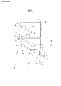
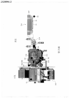
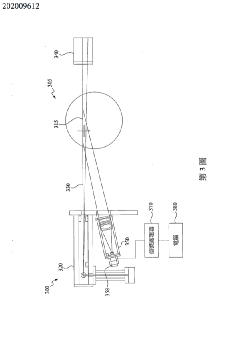
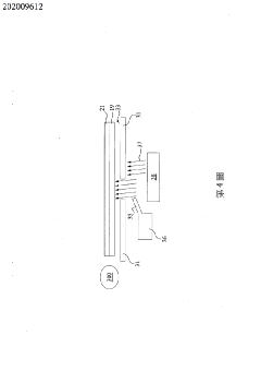
PatentInactiveTW202009612A
Innovation
- Incorporation of sensors at various stages of the EUV lithography system to detect particle generation from membrane rupture, including particle counters, microphones, and acoustic wave sensors, allowing for early detection and localized contamination control.
Supply Chain Resilience for EUV Technology
The EUV lithography supply chain represents one of the most complex and vulnerable technological ecosystems in the semiconductor industry. The highly specialized nature of EUV technology creates significant dependencies on a limited number of suppliers, with ASML holding a virtual monopoly on EUV lithography systems. This concentration of expertise and manufacturing capability presents substantial risks to the global semiconductor industry's ability to maintain Moore's Law progression.
Supply chain vulnerabilities for EUV technology extend across multiple dimensions. Geographic concentration remains a primary concern, with critical components sourced from specific regions including the Netherlands, Germany, Japan, and the United States. Political tensions, trade restrictions, and export controls increasingly threaten the seamless operation of this global supply network, as evidenced by recent US-led restrictions on advanced semiconductor technology transfers to China.
Material constraints further complicate EUV supply chain resilience. The technology relies on rare materials including specialized glass for optics, high-purity gases, and unique chemical compounds for photoresists. Many of these materials have limited sources or require extensive processing capabilities available only in select locations globally. The COVID-19 pandemic exposed how quickly these supply chains can be disrupted, with semiconductor shortages cascading through multiple industries.
Building resilience into the EUV supply chain requires multi-faceted approaches. Leading semiconductor manufacturers have implemented strategic inventory management for critical components, though the high cost and limited shelf life of many EUV materials constrain this strategy. Diversification efforts are underway, with companies investing in alternative suppliers and manufacturing locations where technically feasible, though ASML's core technology remains irreplaceable in the near term.
Industry-government partnerships have emerged as a critical resilience mechanism. The CHIPS Act in the United States, similar initiatives in Europe, and Japan's semiconductor strategy all aim to strengthen domestic capabilities in semiconductor manufacturing, including EUV supply chains. These programs provide funding for research, manufacturing, and workforce development to reduce dependencies on single sources or regions.
Long-term resilience will require continued innovation in manufacturing processes, materials science, and system design. Research into alternative lithography approaches, more durable components, and simplified system architectures may eventually reduce some supply chain vulnerabilities. However, the extreme precision requirements of EUV technology mean that supply chain complexity will remain an inherent challenge as Moore's Law continues to drive semiconductor advancement.
Environmental Impact of EUV Manufacturing
The environmental footprint of EUV lithography manufacturing represents a significant concern as semiconductor technology advances. EUV systems consume substantial energy, with a single lithography machine requiring up to 1 megawatt of power during operation - approximately equivalent to the electricity needs of 800 households. This energy intensity stems primarily from the complex process of generating EUV light, where high-powered lasers strike tin droplets to create the necessary 13.5nm wavelength radiation.
Water usage presents another critical environmental challenge. EUV manufacturing facilities typically consume between 4-5 million gallons of ultra-pure water daily for cooling systems and cleaning processes. This water must undergo extensive purification, further increasing the energy burden and creating wastewater management challenges in regions where semiconductor manufacturing clusters are located.
Chemical consumption in EUV manufacturing introduces additional environmental considerations. The process utilizes various hazardous substances including photoresists, developers, and specialized gases like hydrogen and helium. Many of these materials require careful handling and disposal protocols to prevent environmental contamination. The semiconductor industry has made progress in chemical reduction strategies, but EUV's complex requirements have introduced new challenges.
Carbon emissions associated with EUV manufacturing extend beyond direct energy consumption. The global supply chain supporting EUV technology involves rare earth elements and specialized materials that often require energy-intensive mining and processing operations. A comprehensive lifecycle assessment reveals that the manufacturing phase of EUV equipment contributes approximately 35-40% of its total carbon footprint, with the operational phase accounting for the remainder.
Industry response to these environmental challenges has been multifaceted. Leading manufacturers like ASML have implemented energy recovery systems that capture and reuse waste heat from EUV systems. Water recycling initiatives have demonstrated the potential to reduce freshwater consumption by up to 60% in optimized facilities. Additionally, semiconductor manufacturers are increasingly adopting renewable energy sources to power their operations, with several major players committing to carbon neutrality targets within the next decade.
Regulatory frameworks governing EUV manufacturing vary globally, with the European Union implementing the most stringent environmental standards through directives like the Restriction of Hazardous Substances (RoHS) and Registration, Evaluation, Authorization and Restriction of Chemicals (REACH). As EUV adoption accelerates worldwide, harmonizing these regulations while maintaining technological progress remains a significant industry challenge.
Unlock deeper insights with Patsnap Eureka Quick Research — get a full tech report to explore trends and direct your research. Try now!
Generate Your Research Report Instantly with AI Agent
Supercharge your innovation with Patsnap Eureka AI Agent Platform!