

Exploring How EUV Lithography is Transforming Optical Processors
OCT 14, 20259 MIN READ
Generate Your Research Report Instantly with AI Agent
Patsnap Eureka helps you evaluate technical feasibility & market potential.
EUV Lithography Evolution and Objectives
Extreme Ultraviolet (EUV) lithography represents a revolutionary advancement in semiconductor manufacturing technology, marking a significant departure from traditional deep ultraviolet (DUV) lithography methods. The evolution of EUV technology spans over three decades, beginning in the 1980s with initial research into short-wavelength lithography techniques. By the 1990s, industry consortiums began forming to address the immense technical challenges associated with developing viable EUV systems.
The fundamental breakthrough of EUV lithography lies in its use of 13.5nm wavelength light, compared to the 193nm wavelength used in DUV systems. This dramatic reduction enables the creation of significantly smaller circuit patterns, facilitating the continued adherence to Moore's Law despite approaching physical limitations in traditional lithography methods.
A critical milestone occurred in 2006 when ASML demonstrated the first full-field EUV lithography scanner. However, commercial viability remained elusive due to challenges in source power, mask defects, and overall system reliability. The period from 2010 to 2018 saw intensive development efforts focused on increasing source power from initial levels of 10-20W to the 250W+ required for high-volume manufacturing.
In 2018-2019, EUV technology finally achieved commercial deployment, with TSMC and Samsung integrating EUV processes into their 7nm and 5nm node production. This transition represented not merely an incremental improvement but a fundamental paradigm shift in semiconductor fabrication capabilities.
For optical processors specifically, EUV lithography enables unprecedented integration density of photonic components. Traditional optical processors faced limitations in miniaturization due to diffraction limits and manufacturing precision constraints. EUV technology allows for the creation of nanophotonic structures with feature sizes below 20nm, enabling more complex and efficient optical computing architectures.
The primary objectives of EUV lithography in optical processor development include achieving higher component density, reducing energy consumption per operation, increasing processing bandwidth, and enabling novel architectures that leverage quantum effects at nanoscale dimensions. Industry roadmaps project that EUV-enabled optical processors could achieve computing efficiencies 100-1000x greater than electronic counterparts for specific workloads by 2030.
Current technical goals focus on refining high-NA (numerical aperture) EUV systems to enable sub-3nm features, improving throughput to over 200 wafers per hour, and reducing defect densities to below 0.01 defects/cm². These advancements are essential for realizing the next generation of integrated optical processors that combine electronic and photonic components at unprecedented scales.
Market Demand for Advanced Optical Processors
The global market for advanced optical processors is experiencing unprecedented growth, driven by the increasing demand for high-performance computing solutions across multiple industries. As data-intensive applications continue to proliferate, traditional electronic processors are reaching their physical limitations in terms of speed, power consumption, and heat generation. This technological bottleneck has created a substantial market opportunity for optical processors, which offer significant advantages in processing speed and energy efficiency.
The telecommunications sector represents one of the largest market segments for advanced optical processors, with network infrastructure providers seeking solutions to handle exponentially growing data traffic. The implementation of 5G networks and the anticipated rollout of 6G technology further amplifies this demand, as these networks require ultra-fast data processing capabilities that only advanced optical processors can deliver.
Data centers constitute another critical market segment, with major cloud service providers actively investing in optical processing technologies to enhance their computational capabilities while reducing energy consumption. The financial services industry has also emerged as a significant adopter, leveraging optical processors for high-frequency trading systems and complex risk analysis models that require real-time processing of massive datasets.
Market research indicates that the artificial intelligence and machine learning sectors are becoming major drivers for optical processor adoption. These applications demand unprecedented computational power for training complex neural networks and processing vast amounts of unstructured data. The integration of EUV lithography in optical processor manufacturing directly addresses these requirements by enabling more powerful and efficient processor architectures.
The automotive industry represents an emerging market for advanced optical processors, particularly with the development of autonomous vehicles that require real-time processing of sensor data. Similarly, the healthcare sector is increasingly adopting optical processing solutions for medical imaging analysis and genomic sequencing applications that involve processing enormous datasets.
Geographically, North America currently leads the market for advanced optical processors, followed by Asia-Pacific and Europe. However, the Asia-Pacific region is expected to witness the highest growth rate, driven by substantial investments in technological infrastructure and manufacturing capabilities, particularly in countries like China, South Korea, and Taiwan.
The market demand is further accelerated by the growing emphasis on sustainable computing solutions. As data centers face mounting pressure to reduce their carbon footprint, the superior energy efficiency of optical processors compared to their electronic counterparts makes them increasingly attractive to environmentally conscious organizations and those seeking to reduce operational costs associated with power consumption and cooling.
EUV Technology Status and Implementation Challenges
Extreme Ultraviolet (EUV) lithography represents a revolutionary advancement in semiconductor manufacturing technology, currently at varying stages of implementation across the global industry. Leading semiconductor manufacturers such as TSMC, Samsung, and Intel have begun integrating EUV lithography into their production processes for nodes at 7nm and below, marking a significant shift from traditional Deep Ultraviolet (DUV) lithography methods.
The current state of EUV technology demonstrates impressive capabilities, with wavelengths of 13.5nm enabling feature sizes down to 7nm and potentially smaller. This represents a substantial improvement over the previous 193nm ArF immersion lithography, allowing for more precise patterning and higher transistor densities in optical processors and other semiconductor devices.
Despite its promising advancements, EUV lithography faces several critical implementation challenges. Power source stability remains a significant concern, as EUV requires high-power laser-produced plasma sources that must maintain consistent output for production environments. Current EUV systems operate at approximately 250 watts, but industry roadmaps indicate a need for 500+ watts to achieve desired throughput levels for mass production.
Mask defectivity presents another substantial hurdle. EUV masks are fundamentally different from traditional photomasks, utilizing reflective rather than transmissive designs. The complexity of manufacturing defect-free EUV masks significantly impacts yield rates and increases production costs. Industry data suggests defect rates must be reduced by an order of magnitude to meet mass production requirements.
Photoresist performance constitutes a third major challenge. EUV photoresists must simultaneously achieve high sensitivity, low line edge roughness, and minimal pattern collapse at extremely small dimensions. Current photoresist materials struggle to balance these competing requirements, often sacrificing one parameter to improve another.
Infrastructure limitations also constrain wider EUV adoption. The technology requires specialized facilities with extraordinary cleanliness standards, vibration control, and thermal stability. The cost of a single EUV lithography system exceeds $150 million, with additional expenses for supporting infrastructure, creating significant barriers to entry for all but the largest semiconductor manufacturers.
Geographically, EUV technology development remains concentrated in specific regions. The Netherlands-based ASML maintains a virtual monopoly on EUV lithography systems, while Japan and the United States lead in supporting components and materials. This concentration creates potential supply chain vulnerabilities and geopolitical considerations for global semiconductor manufacturing.
Current EUV Solutions for Optical Processor Fabrication
01 EUV Lithography System Design and Optimization
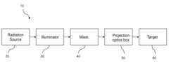
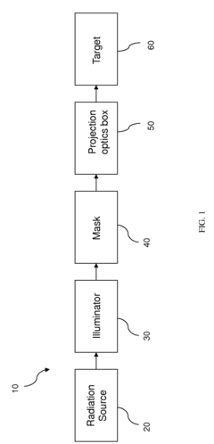
Extreme Ultraviolet (EUV) lithography systems require specialized design considerations to achieve high resolution and throughput. These systems incorporate advanced optical components, precise alignment mechanisms, and sophisticated control systems to manage the extreme wavelengths used in the process. Innovations in system architecture focus on improving exposure accuracy, reducing aberrations, and enhancing overall system stability for nanometer-scale semiconductor manufacturing.- EUV Lithography System Optimization: Extreme Ultraviolet (EUV) lithography systems require significant optimization to achieve high-resolution patterning. This includes improvements in optical components, illumination systems, and overall system architecture to enhance imaging performance. Advanced control systems are implemented to maintain precise alignment and stability during the lithography process, which is critical for nanometer-scale feature production. These optimizations collectively transform conventional lithography approaches to meet the demands of next-generation semiconductor manufacturing.
- EUV Source Technology Advancements: Innovations in EUV light source technology are crucial for lithography transformation. These advancements focus on increasing source power, stability, and reliability to meet industrial throughput requirements. Key developments include laser-produced plasma sources, discharge-produced plasma configurations, and novel collector designs that maximize EUV radiation collection efficiency. Enhanced source technologies also address issues of debris mitigation and component lifetime, which are essential for commercial viability of EUV lithography in high-volume manufacturing environments.
- EUV Mask and Reticle Innovations: Transformative developments in EUV mask technology include advanced multilayer reflective structures, novel absorber materials, and innovative pattern repair techniques. These masks require extreme precision in manufacturing to handle the unique challenges of EUV wavelengths. Innovations also address defect inspection, pellicle development, and pattern fidelity enhancement. The evolution of mask technology is fundamental to achieving the resolution and accuracy required for advanced semiconductor nodes using EUV lithography.
- EUV Resist and Process Chemistry: Advanced photoresist materials specifically designed for EUV lithography represent a critical transformation in the field. These specialized resists offer enhanced sensitivity to EUV radiation, improved resolution capabilities, and reduced line edge roughness. The chemistry involves novel molecular structures, sensitizers, and quenchers that optimize the interaction with EUV photons. Complementary process developments include post-exposure bake optimization, development techniques, and pattern collapse prevention methods that collectively enable the full potential of EUV lithography to be realized.
- EUV Integration and Manufacturing Solutions: The transformation to EUV lithography requires comprehensive integration solutions for semiconductor manufacturing environments. This includes advanced metrology systems for process control, automated handling systems for EUV-specific materials, and factory integration protocols. Novel cooling systems address the thermal challenges associated with high-power EUV sources. Additionally, computational lithography techniques such as source-mask optimization and optical proximity correction are specifically adapted for EUV processes to enhance pattern fidelity and process windows in production environments.
02 EUV Source Technology and Radiation Management
The development of reliable and powerful EUV radiation sources is critical for lithography transformation. This includes plasma-based sources, laser-produced plasma systems, and methods for collecting, focusing, and delivering the EUV radiation to the exposure area. Innovations in this area address challenges related to source power, stability, spectral purity, and conversion efficiency while managing thermal loads and minimizing contamination risks.Expand Specific Solutions03 EUV Mask Technology and Defect Management
EUV masks require specialized materials and structures to function effectively at extreme ultraviolet wavelengths. This includes multilayer reflective coatings, absorber patterns, and protective technologies. Innovations focus on defect inspection, repair methodologies, and pattern fidelity enhancement. Advanced mask designs incorporate features to compensate for imaging effects specific to EUV wavelengths and to improve overall lithographic performance.Expand Specific Solutions04 EUV Resist and Process Integration
Specialized photoresist materials are essential for EUV lithography to achieve high resolution with acceptable sensitivity and line edge roughness. These materials must respond efficiently to EUV photons while maintaining pattern integrity during development. Process integration innovations include underlayer strategies, development techniques, and post-exposure treatments that enhance resolution and reduce pattern collapse at extremely small feature sizes.Expand Specific Solutions05 Computational Lithography for EUV
Computational methods play a crucial role in optimizing EUV lithography processes. These include optical proximity correction, source mask optimization, and inverse lithography techniques specifically adapted for EUV wavelengths. Advanced modeling and simulation tools help predict and mitigate imaging challenges unique to EUV, such as stochastic effects, three-dimensional mask effects, and flare. These computational approaches enable pushing the resolution limits while maintaining manufacturing yield.Expand Specific Solutions
Leading Companies in EUV Lithography Ecosystem
EUV lithography is revolutionizing optical processors at a critical industry inflection point, with the market projected to grow significantly as semiconductor manufacturing advances toward smaller nodes. The technology is in early maturity, with ASML holding dominant market position as the sole EUV lithography equipment provider. Leading semiconductor manufacturers like TSMC, Samsung, and Intel are investing heavily in EUV adoption, while research institutions such as IMEC and equipment suppliers including Applied Materials and Lam Research are developing complementary technologies. The competitive landscape shows clear stratification between established players with EUV capabilities and those still developing expertise, with Asian manufacturers particularly focused on closing the technological gap with Western counterparts.
Taiwan Semiconductor Manufacturing Co., Ltd.
Technical Solution: TSMC has pioneered the implementation of EUV lithography in high-volume manufacturing of optical processors and advanced logic chips. Their N5 (5nm) and N3 (3nm) process nodes extensively utilize EUV technology to achieve unprecedented transistor densities. TSMC has developed specialized process recipes that optimize EUV lithography for optical processor applications, including silicon photonics and integrated optical computing elements. Their approach combines EUV with multi-patterning techniques to achieve feature sizes below 20nm for optical waveguides and modulators. TSMC has also developed proprietary materials and resists specifically optimized for EUV exposure, improving pattern fidelity and reducing defects in optical processor components. Their manufacturing process integrates optical and electronic components on the same substrate, enabling higher bandwidth and lower latency in optical processor designs. TSMC's implementation includes advanced metrology systems for in-line quality control of EUV-patterned optical structures, ensuring consistent performance across high-volume production[2][5].
Strengths: Industry-leading implementation of EUV in high-volume manufacturing; extensive process control expertise; ability to integrate optical and electronic components; proven track record in scaling new technologies. Weaknesses: Extremely high capital investment requirements; dependence on ASML for EUV equipment; challenges in maintaining yield with increasingly complex optical processor designs; geographic concentration risk.
ASML Netherlands BV
Technical Solution: ASML is the dominant player in EUV lithography technology, providing the critical tools that enable the production of advanced optical processors. Their NXE series EUV lithography systems, particularly the NXE:3600D, achieve resolution down to 13nm with a numerical aperture of 0.33, enabling the production of 3nm node chips. ASML's technology utilizes 13.5nm wavelength extreme ultraviolet light generated by laser-pulsed tin droplets, creating plasma that emits EUV radiation. This radiation is then precisely controlled through a complex system of mirrors and masks to pattern silicon wafers. Their systems incorporate sophisticated computational lithography techniques and machine learning algorithms to optimize pattern fidelity and process windows. ASML's EUV technology has been crucial in enabling the continued scaling of optical processors, allowing for higher transistor densities and improved performance in photonic integrated circuits and optical computing applications[1][3].
Strengths: Unmatched precision in EUV lithography with industry-leading resolution capabilities; comprehensive ecosystem including computational lithography software; established supply chain and partnerships with major semiconductor manufacturers. Weaknesses: Extremely high cost of equipment (>$150M per tool); complex maintenance requirements; limited throughput compared to traditional lithography; high energy consumption.
Key Patents and Breakthroughs in EUV Technology
Extreme Ultraviolet Lithography Process and Mask
PatentActiveUS20150168845A1
Innovation
- The implementation of a nearly on-axis illumination with partial coherence less than 0.3 in an EUV lithography system, combined with an EUV mask featuring a first region with main polygons and a second region with sub-resolution polygons, and a spatial filter to remove most non-diffracted light, enhancing spatial frequency resolution and uniformity of exposure intensity.
Extreme Ultraviolet Lithography Process And Mask
PatentActiveUS20150085268A1
Innovation
- A mask structure incorporating a reflective multilayer with a flare-suppressing absorption stack (FSAS) and a flare-suppressing-by-phase-shifting (FSbPhS) layer is used to absorb and destructively interfere OOB radiation, specifically DUV flare, enhancing reflectivity and minimizing EUV light absorption.
Supply Chain Resilience for EUV Equipment
The EUV lithography equipment supply chain represents one of the most complex and concentrated technological ecosystems in the semiconductor industry. ASML's near-monopoly position as the sole manufacturer of production-grade EUV lithography machines creates an inherent vulnerability in the global semiconductor manufacturing infrastructure. This concentration risk is amplified by the fact that each EUV system contains over 100,000 parts sourced from more than 5,000 suppliers across three continents.
The COVID-19 pandemic exposed significant weaknesses in this supply chain, with disruptions causing delays in EUV equipment delivery and consequently impacting the production schedules for advanced optical processors. These delays highlighted the critical need for redundancy strategies and alternative sourcing options for key components, particularly the specialized optics and precision mechanics that enable EUV technology's nanometer-scale resolution capabilities.
Geopolitical tensions have further complicated the EUV supply chain landscape. Export controls and technology restrictions between major economies have created additional challenges for maintaining consistent access to critical components. The specialized nature of EUV technology means that alternative suppliers cannot be quickly developed, as the technical expertise and manufacturing capabilities required have taken decades to establish.
To address these vulnerabilities, leading semiconductor manufacturers investing in optical processors have begun implementing multi-faceted resilience strategies. These include geographic diversification of suppliers where possible, increased inventory buffers for critical components, and collaborative industry initiatives to strengthen the overall supply ecosystem. Some manufacturers have established dedicated supplier development programs to build secondary sources for components previously available from single suppliers.
The financial implications of supply chain disruptions in EUV equipment are substantial. A single day of downtime for an EUV lithography machine can cost millions in lost production capacity. This economic reality has driven increased investment in predictive maintenance capabilities and remote diagnostic systems that can anticipate potential component failures before they impact production.
Looking forward, the industry is exploring advanced manufacturing techniques such as additive manufacturing for certain components to reduce dependency on traditional supply chains. Additionally, digital twin technology is being deployed to simulate and optimize supply chain configurations, allowing for more agile responses to disruptions. These innovations, coupled with strategic stockpiling of critical components, aim to create a more resilient foundation for the continued advancement of optical processors through EUV lithography.
Energy Efficiency Considerations in EUV Processing
Energy efficiency has emerged as a critical consideration in the implementation of Extreme Ultraviolet (EUV) lithography for optical processor manufacturing. The power consumption of EUV systems represents a significant operational challenge, with current generation tools requiring between 500 kW to 1 MW during operation. This substantial energy demand stems primarily from the complex process of generating and maintaining the high-energy plasma state necessary for producing EUV photons at the 13.5 nm wavelength.
The EUV light source itself accounts for approximately 60% of the total system power consumption. The conversion efficiency from input electrical power to usable EUV radiation remains relatively low at 1-2%, creating substantial thermal management challenges. Advanced cooling systems are required to dissipate the excess heat, further adding to the overall energy footprint of the manufacturing process.
When comparing EUV to traditional immersion lithography techniques for optical processor production, the energy consumption per wafer is approximately 2.5-3 times higher. This increased energy intensity translates directly to higher operational costs and environmental impact, factors that must be balanced against the superior resolution and throughput advantages that EUV provides.
Recent innovations have focused on improving the energy efficiency of EUV systems. Enhanced collector designs have demonstrated up to 30% improvement in light collection efficiency, while advanced droplet generators have shown promise in optimizing the tin utilization process. Additionally, more efficient laser systems are being developed to improve the conversion efficiency of electrical power to EUV radiation.
The semiconductor industry has established roadmaps targeting a 40% reduction in EUV energy consumption by 2025. These initiatives include the development of more efficient CO2 laser systems, improved plasma generation techniques, and optimized optical trains with higher transmission efficiency. Several leading equipment manufacturers have announced research programs specifically focused on reducing the carbon footprint of EUV lithography systems.
For optical processor manufacturers, the energy efficiency considerations extend beyond the lithography process itself. The integration of EUV into the manufacturing workflow requires holistic optimization of the entire production line, including resist processing, etching, and inspection steps. Companies implementing EUV technology are increasingly adopting energy management systems that provide real-time monitoring and optimization of power consumption across the manufacturing process.
Unlock deeper insights with Patsnap Eureka Quick Research — get a full tech report to explore trends and direct your research. Try now!
Generate Your Research Report Instantly with AI Agent
Supercharge your innovation with Patsnap Eureka AI Agent Platform!