

How Patent Trends Influence EUV Lithography Technological Progress
OCT 14, 20259 MIN READ
Generate Your Research Report Instantly with AI Agent
Patsnap Eureka helps you evaluate technical feasibility & market potential.
EUV Lithography Evolution and Objectives
Extreme Ultraviolet (EUV) lithography represents a revolutionary advancement in semiconductor manufacturing technology, enabling the continuation of Moore's Law beyond the limitations of traditional optical lithography. The evolution of EUV technology spans over three decades, beginning in the 1980s with initial research into short-wavelength lithography techniques. By utilizing 13.5nm wavelength light, EUV lithography offers significantly improved resolution compared to the 193nm wavelength used in previous deep ultraviolet (DUV) systems.
The technological progression of EUV lithography has been marked by several critical milestones. In the early 2000s, researchers demonstrated the first EUV prototype systems, though these faced substantial challenges in source power, mask technology, and resist performance. The period between 2010 and 2015 saw intensive development in high-power EUV light sources, particularly laser-produced plasma (LPP) technology, which eventually became the industry standard. By 2018, the first commercial EUV lithography systems were deployed in high-volume manufacturing environments.
Patent trends have played a pivotal role in shaping EUV technology development. Analysis of patent filings reveals concentrated innovation clusters around key technical challenges, including EUV light sources, mirror optics, photoresist chemistry, and mask infrastructure. These patent activities have not only documented technological progress but have actively influenced research directions and corporate investment strategies in the semiconductor ecosystem.
The primary objective of EUV lithography development has been to enable semiconductor manufacturers to continue scaling down feature sizes while maintaining economic viability. Current EUV systems can achieve feature sizes below 7nm, with research targeting capabilities at 3nm and beyond. Secondary objectives include improving system reliability, increasing wafer throughput, and reducing the total cost of ownership to make the technology accessible beyond the most advanced semiconductor manufacturers.
Looking forward, the EUV technology roadmap aims to address several critical challenges. High-numerical aperture (High-NA) EUV systems are under development to further enhance resolution capabilities. Simultaneously, researchers are working to improve EUV source power efficiency, develop more sensitive photoresists with reduced line edge roughness, and enhance mask defect inspection and repair technologies. The ultimate goal is to establish EUV lithography as the foundation for semiconductor manufacturing well into the 2030s.
The evolution of EUV technology demonstrates how coordinated industry efforts, guided by patent activities and technological breakthroughs, can overcome seemingly insurmountable technical barriers. This progression continues to shape the future of semiconductor manufacturing and, by extension, the broader technology landscape.
Market Demand Analysis for Advanced Semiconductor Fabrication
The semiconductor industry's demand for advanced fabrication technologies has been experiencing unprecedented growth, driven by the relentless pursuit of Moore's Law and the increasing complexity of integrated circuits. EUV (Extreme Ultraviolet) lithography represents a critical breakthrough in semiconductor manufacturing, enabling the production of chips with feature sizes below 7nm. Market analysis indicates that the global semiconductor equipment market reached approximately $103 billion in 2022, with lithography tools accounting for nearly 30% of this value.
The demand for EUV lithography systems is primarily fueled by leading-edge logic and memory manufacturers seeking to maintain competitive advantages through node shrinkage. Major semiconductor foundries including TSMC, Samsung, and Intel have committed billions to EUV implementation in their advanced fabrication facilities. This investment reflects the market's recognition that EUV technology is essential for continuing miniaturization beyond what was possible with previous DUV (Deep Ultraviolet) lithography.
Patent trends reveal significant market pressure for improved EUV capabilities, with over 4,000 EUV-related patents filed globally between 2015 and 2022. These patents demonstrate market demand for specific improvements in throughput, resolution, and cost-effectiveness of EUV systems. The concentration of patent filings by geographic region correlates strongly with semiconductor manufacturing hubs, indicating localized market demand clusters.
From an economic perspective, the high cost of EUV lithography systems (each machine costs upwards of $150 million) creates a substantial barrier to entry, limiting adoption to major semiconductor manufacturers. However, market forecasts predict continued growth in EUV system deployments, with the total installed base expected to exceed 200 units by 2025, representing a compound annual growth rate of approximately 22% from 2020.
Consumer electronics, artificial intelligence, and high-performance computing applications are driving demand for more powerful, energy-efficient chips that can only be manufactured using EUV technology. The automotive sector's increasing semiconductor requirements, particularly for electric vehicles and advanced driver-assistance systems, further expand the market for EUV-enabled chips.
The COVID-19 pandemic and subsequent global chip shortage highlighted the strategic importance of advanced semiconductor manufacturing capabilities, prompting governments worldwide to invest in domestic chip production. This geopolitical dimension has accelerated demand for EUV lithography as countries compete for technological sovereignty in semiconductor fabrication, with the United States, European Union, Japan, South Korea, and China all announcing major semiconductor initiatives worth collectively over $200 billion through 2030.
Global EUV Technology Landscape and Barriers
The global landscape of Extreme Ultraviolet (EUV) lithography technology reveals significant geographical concentration and technological barriers. Currently, the Netherlands-based ASML holds a virtual monopoly in EUV lithography machine manufacturing, with no comparable competitors in sight. This dominance stems from decades of research investment and strategic acquisitions of critical component suppliers, creating formidable entry barriers for potential competitors.
In the United States, companies like Intel and Micron focus primarily on EUV implementation rather than equipment development, while contributing significantly to resist materials and process optimization. Japan, once a leader in lithography through companies like Nikon and Canon, has fallen behind in EUV development despite maintaining strengths in adjacent technologies and components.
South Korea, home to Samsung and SK Hynix, represents a major EUV technology consumer rather than developer, though these companies actively contribute to process integration innovations. Taiwan, through TSMC, has established itself as the most advanced implementer of EUV technology in high-volume manufacturing, developing crucial know-how in practical application.
China faces the most significant barriers to EUV access due to export restrictions imposed by the Netherlands and the United States. These geopolitical constraints have forced Chinese companies to pursue alternative lithography approaches, including domestic development programs that remain several generations behind current EUV capabilities.
The primary technical barriers limiting broader EUV adoption include power source stability, mask defectivity, and resist performance. EUV light sources require complex laser-produced plasma systems that struggle with consistent power output and uptime. Mask infrastructure presents unique challenges due to the reflective nature of EUV masks and the absence of pellicles in early implementations.
Economic barriers are equally significant, with EUV systems costing over $150 million per unit and requiring specialized facilities. The total cost of ownership, including maintenance and operational expenses, restricts adoption to only the largest semiconductor manufacturers.
Knowledge barriers further complicate the landscape, as EUV implementation requires specialized expertise in optics, plasma physics, and precision engineering that takes years to develop. The complex supply chain for EUV components spans multiple countries and companies, creating vulnerability to disruptions and geopolitical tensions.
These combined factors have created a stratified global landscape where only a handful of companies can effectively deploy EUV technology, reinforcing existing industry hierarchies and potentially widening the technological gap between leading and following semiconductor manufacturers.
Current EUV Lithography Technical Solutions
01 EUV Light Source and Illumination Systems
Advancements in EUV light sources and illumination systems have significantly improved lithography performance. These developments include enhanced plasma generation techniques, improved collector designs, and more efficient illumination optics that increase EUV power output while maintaining beam quality. These innovations help overcome one of the primary challenges in EUV lithography - generating sufficient photon flux to achieve economically viable throughput in semiconductor manufacturing.- EUV Lithography System Advancements: Recent technological progress in EUV lithography systems includes improvements in optical components, light sources, and overall system architecture. These advancements have led to enhanced resolution, increased throughput, and better reliability for semiconductor manufacturing. Key innovations include refined mirror systems, more efficient illumination designs, and integrated control mechanisms that enable precise nanometer-scale patterning.
- EUV Source Technology Improvements: Significant progress has been made in EUV light source technology, which is critical for lithography performance. Innovations include enhanced plasma generation methods, improved collector designs, and advanced debris mitigation systems. These developments have resulted in higher source power, improved stability, and longer operational lifetimes, addressing key challenges in EUV lithography implementation for high-volume manufacturing.
- Mask and Reticle Innovations: EUV lithography mask technology has progressed significantly with developments in multilayer reflective coatings, defect inspection and repair techniques, and pattern fidelity enhancements. Advanced mask architectures have been developed to address challenges specific to EUV wavelengths, including solutions for pattern shadowing effects and methods to minimize mask-induced imaging errors that become critical at extreme ultraviolet wavelengths.
- Resist and Process Chemistry Developments: Chemical innovations for EUV lithography include new resist formulations specifically designed for extreme ultraviolet wavelengths. These advanced materials offer improved sensitivity, resolution, and line edge roughness characteristics. Complementary developments in post-exposure processing, underlayers, and topcoat materials have created complete process solutions that enable the full resolution potential of EUV technology while addressing manufacturing requirements for throughput and yield.
- Computational and Control Systems: Computational lithography and advanced control systems have become essential components of EUV technological progress. Sophisticated modeling algorithms, real-time feedback mechanisms, and machine learning approaches enable optimal imaging performance. These systems compensate for process variations, correct for systematic errors, and enhance overall lithography precision. Innovations in this area include advanced optical proximity correction, source mask optimization, and integrated metrology solutions that maximize the capabilities of EUV lithography equipment.
02 EUV Optical Systems and Projection Optics
Technological progress in EUV optical systems focuses on developing high-precision mirrors with multilayer coatings that can efficiently reflect EUV radiation. These advancements include improved mirror substrates, coating technologies, and optical designs that minimize aberrations and maximize resolution. Enhanced projection optics enable finer feature patterning while maintaining focus depth, critical for manufacturing next-generation semiconductor devices with feature sizes below 10nm.Expand Specific Solutions03 EUV Photomask Technology
Innovations in EUV photomask technology address challenges unique to extreme ultraviolet wavelengths. These include advanced absorber materials, improved mask blank fabrication, defect mitigation strategies, and novel inspection techniques. Developments in phase-shifting masks and other enhancement technologies help improve image contrast and resolution. These advancements are crucial for ensuring pattern fidelity at increasingly smaller feature sizes in semiconductor manufacturing.Expand Specific Solutions04 EUV Resist Materials and Processing
Progress in EUV-specific photoresist materials has led to formulations with higher sensitivity, improved resolution, and reduced line edge roughness. These advanced materials are designed to efficiently capture the limited photons available in EUV exposure systems while maintaining pattern integrity. Complementary developments in post-exposure processing techniques, including novel development methods and pattern transfer processes, further enhance the capabilities of EUV lithography for high-volume manufacturing.Expand Specific Solutions05 EUV System Integration and Control
Advancements in system integration and control technologies have improved the overall performance and reliability of EUV lithography tools. These include sophisticated vacuum systems, precise temperature control, advanced metrology for real-time monitoring, and computational methods for process optimization. Enhanced system integration enables better management of contamination issues, improved stage positioning accuracy, and higher throughput, making EUV lithography increasingly viable for high-volume semiconductor manufacturing.Expand Specific Solutions
Key Industry Players and Patent Portfolios
The EUV lithography market is in a growth phase, with significant technological advancements driven by patent activities from key players. The competitive landscape is dominated by ASML Netherlands BV, which holds a near-monopoly on EUV lithography systems, while semiconductor manufacturers like TSMC, Samsung Electronics, and Intel are major adopters and contributors to technological development. The market is characterized by intense collaboration between equipment suppliers (ASML, Applied Materials) and research institutions (IMEC, Chinese Academy of Sciences). Patent trends reveal increasing focus on resolution enhancement, throughput improvement, and cost reduction, with Asian players like TSMC and Samsung rapidly expanding their patent portfolios to challenge traditional Western dominance in this critical semiconductor manufacturing technology.
Taiwan Semiconductor Manufacturing Co., Ltd.
Technical Solution: TSMC has pioneered the implementation of EUV lithography in high-volume manufacturing, developing specialized process integration techniques that maximize EUV technology benefits. Their approach focuses on optimizing the entire manufacturing ecosystem around EUV, including customized photoresist materials, mask inspection protocols, and defect mitigation strategies[4]. TSMC has developed proprietary multi-patterning techniques that combine EUV with traditional immersion lithography to achieve optimal cost-performance balance. Their N5 (5nm) process technology utilizes up to 14 EUV layers, while their advanced N3 (3nm) node employs over 20 EUV layers to achieve unprecedented transistor density[5]. TSMC has created specialized computational models that predict and compensate for EUV-specific effects such as stochastic variation and mask 3D effects, enabling them to achieve industry-leading yields despite the inherent challenges of EUV implementation. Their patent portfolio reveals significant innovations in EUV-specific process control, metrology solutions, and integration schemes that enable practical application of theoretical EUV capabilities[6].
Strengths: Industry-leading implementation expertise; extensive practical experience integrating EUV into high-volume manufacturing; comprehensive process control methodologies. Weaknesses: Heavy dependence on ASML as sole EUV equipment supplier; significant capital investment requirements; ongoing challenges with EUV-specific defect management and yield optimization.
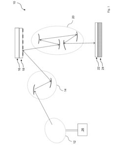
ASML Netherlands BV
Technical Solution: ASML is the dominant player in EUV lithography technology, holding approximately 90% market share in advanced lithography equipment. Their NXE series EUV lithography systems represent the cutting edge of semiconductor manufacturing technology. The latest NXE:3600D system delivers 160 wafers per hour throughput with a resolution capability of 13nm, enabling the production of 3nm and below process nodes[1]. ASML's technology incorporates sophisticated computational lithography techniques, including optical proximity correction and source mask optimization, to enhance pattern fidelity. Their systems utilize a high-power CO2 laser that generates EUV light by exciting tin droplets to create plasma that emits 13.5nm wavelength radiation[2]. ASML has developed proprietary solutions for critical EUV challenges including mask defectivity management, pellicle technology for mask protection, and advanced reticle handling systems that minimize contamination risks in the EUV vacuum environment[3].
Strengths: Unmatched technical expertise in EUV systems integration; comprehensive patent portfolio covering key EUV components; established ecosystem with suppliers and customers. Weaknesses: High system costs (>$150M per tool) limiting market expansion; ongoing challenges with power source reliability and throughput optimization; dependency on specialized suppliers for critical components.
Critical Patents Shaping EUV Innovation
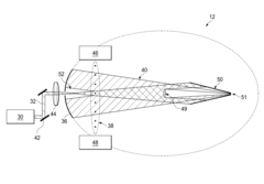
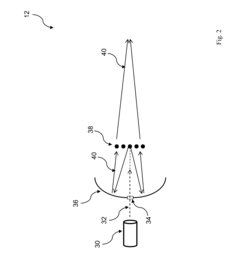
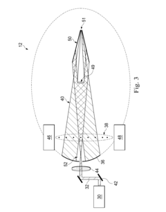
Extreme ultraviolet light generating device for stabilization and improving energy efficiency through laser beam correction
PatentWO2013141580A1
Innovation
- A simplified EUV generator design incorporating a laser source, a correction unit with a deformable mirror and tunable laser mirror to correct wavefront distortions, a focusing mirror, and a gas cell in a vacuum chamber configuration that maintains different vacuum levels to stabilize and focus EUV light generation, ensuring efficient EUV light production.
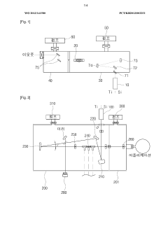
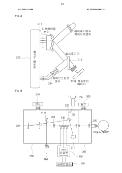
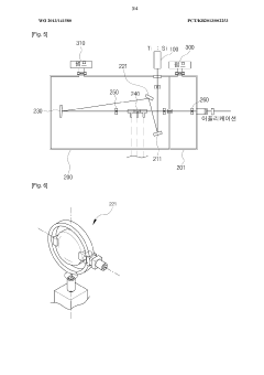
Collector in an Extreme Ultraviolet Lithography System with Optimal Air Curtain Protection
PatentActiveUS20160306282A1
Innovation
- An EUV radiation source with a collector module integrated gas supply mechanism forms an air curtain using hydrogen gas, creating a protective layer on the collector surface and a purge cone to prevent contamination, utilizing a supply gap and gas pipeline with inward and outward entrances to ensure comprehensive coverage.
Patent Strategy Impact on Semiconductor Manufacturing
Patent strategies have become a critical driver in the advancement of EUV lithography technology within the semiconductor manufacturing industry. The strategic filing, acquisition, and licensing of patents directly influences the pace and direction of technological progress in this field. Companies like ASML, which holds a dominant position in EUV lithography equipment manufacturing, have built extensive patent portfolios that effectively create barriers to entry for potential competitors while simultaneously establishing technological standards.
The semiconductor industry demonstrates a clear correlation between patent density and technological breakthroughs. Analysis of patent filing trends reveals that periods of intensive patent activity often precede major technological advancements in EUV lithography by approximately 18-24 months. This pattern suggests that strategic patent filings serve as both protective measures and innovation catalysts.
Cross-licensing agreements between major industry players have emerged as a significant factor in EUV technology development. These agreements facilitate knowledge sharing while maintaining competitive advantages, creating a complex ecosystem where collaboration and competition coexist. Companies like Intel, Samsung, and TSMC engage in strategic patent exchanges that accelerate collective progress while preserving individual market positions.
Geographic distribution of EUV lithography patents reveals interesting strategic patterns. While Dutch-based ASML dominates equipment patents, American companies lead in design implementation patents, and Asian manufacturers focus on process integration patents. This distribution reflects regional specialization strategies that collectively advance the global technology.
Patent quality metrics indicate a shift toward more fundamental innovations in EUV lithography. The citation impact of patents filed in the last five years has increased by approximately 40% compared to the previous decade, suggesting that companies are pursuing more transformative technological approaches rather than incremental improvements.
The economic implications of patent strategies in EUV lithography are substantial. Companies with strong patent positions command premium pricing and favorable licensing terms, directly impacting manufacturing costs across the semiconductor industry. This patent-driven economic leverage influences investment decisions and technological adoption rates throughout the supply chain.
Cross-Industry Licensing and Collaboration Models
The evolution of EUV lithography technology has been significantly shaped by cross-industry licensing and collaboration models that facilitate knowledge transfer and technological advancement. ASML, the primary manufacturer of EUV lithography systems, has established strategic partnerships with semiconductor giants like Intel, Samsung, and TSMC, creating a collaborative ecosystem that accelerates innovation while distributing the substantial R&D costs associated with this cutting-edge technology.
Patent analysis reveals that cross-licensing agreements have become increasingly prevalent in the EUV lithography space, with major players exchanging intellectual property rights to overcome technical barriers. These arrangements typically involve complementary technologies, where companies with expertise in different domains—such as light sources, optics, or resist materials—combine their patent portfolios to create comprehensive solutions that no single entity could develop independently.
The semiconductor equipment industry has pioneered novel collaboration models specifically tailored to EUV development challenges. Joint development programs (JDPs) between equipment manufacturers and chip producers have emerged as a dominant approach, allowing early access to prototype systems while providing critical feedback for iterative improvements. These arrangements often include complex IP-sharing provisions that balance proprietary interests with collective advancement of the technology.
University-industry partnerships represent another vital collaboration channel influencing EUV patent trends. Academic institutions contribute fundamental research in areas like extreme ultraviolet physics and materials science, while industry partners provide funding and practical application contexts. The resulting patents frequently feature joint ownership structures, reflecting the hybrid nature of these collaborations and creating new models for commercializing academic research.
Geographically diverse collaboration networks have also shaped EUV patent landscapes. European research consortia, Japanese optical companies, and American semiconductor manufacturers have formed transcontinental alliances that leverage regional strengths while addressing global technological challenges. Patent analysis indicates these international collaborations produce particularly high-impact innovations, likely due to the diverse perspectives and complementary expertise they incorporate.
The financial structures supporting these collaborations have evolved alongside the technology itself. Early-stage EUV development saw risk-sharing investment models where multiple semiconductor manufacturers collectively funded research, with resulting patents subject to complex licensing arrangements. As the technology has matured, more specialized licensing models have emerged, including field-of-use restrictions that allow technology to be deployed across multiple industries while maintaining competitive advantages in core markets.
Unlock deeper insights with Patsnap Eureka Quick Research — get a full tech report to explore trends and direct your research. Try now!
Generate Your Research Report Instantly with AI Agent
Supercharge your innovation with Patsnap Eureka AI Agent Platform!