How Do Regulations Affect the Adoption of EUV Lithography
OCT 14, 20259 MIN READ
Generate Your Research Report Instantly with AI Agent
Patsnap Eureka helps you evaluate technical feasibility & market potential.
EUV Lithography Background and Objectives
Extreme Ultraviolet (EUV) lithography represents a revolutionary advancement in semiconductor manufacturing technology, enabling the production of increasingly smaller and more powerful microchips. The development of EUV lithography began in the 1990s as traditional deep ultraviolet (DUV) lithography approached its physical limits. This technology utilizes light with a wavelength of 13.5 nanometers, significantly shorter than the 193-nanometer wavelength used in DUV lithography, allowing for the creation of semiconductor features below 7 nanometers.
The evolution of EUV technology has been marked by significant technical challenges, including the development of suitable light sources, mirrors, photoresists, and masks. Early research was primarily conducted by consortia such as SEMATECH and ASML in collaboration with research institutions. By the mid-2010s, ASML emerged as the dominant player in EUV lithography equipment manufacturing, with their first commercial EUV systems being shipped in 2017.
Current technological trends indicate a continued push toward smaller node sizes, with leading semiconductor manufacturers implementing EUV lithography for 7nm, 5nm, and now 3nm process nodes. The industry roadmap suggests further refinements to enable 2nm and potentially 1nm nodes in the coming years, though each advancement brings exponentially greater technical challenges.
The primary objective of EUV lithography implementation is to maintain the trajectory predicted by Moore's Law, which has historically guided semiconductor advancement. However, the technology also aims to address efficiency concerns, as multiple patterning techniques required with DUV lithography become increasingly complex and costly at smaller nodes.
From a regulatory perspective, EUV lithography exists within a complex ecosystem of international trade regulations, export controls, and national security considerations. The technology is considered dual-use, having both commercial and potential military applications, which has led to its inclusion in various export control regimes such as the Wassenaar Arrangement.
The strategic importance of EUV lithography in maintaining technological leadership has elevated it to a geopolitical concern, particularly in the context of US-China technology competition. This has resulted in increasingly stringent regulations affecting the global supply chain for EUV equipment and related technologies, creating a complex landscape for technology adoption across different regions.
The regulatory environment surrounding EUV lithography continues to evolve, with implications for technology transfer, intellectual property protection, and market access that directly impact the pace and pattern of adoption worldwide.
Market Demand Analysis for EUV Technology
The global market for Extreme Ultraviolet (EUV) lithography technology has witnessed substantial growth in recent years, driven primarily by the semiconductor industry's relentless pursuit of Moore's Law. As chip manufacturers strive to produce smaller, more powerful, and energy-efficient semiconductors, EUV technology has emerged as the critical enabler for advanced node production below 7nm. Market research indicates that the EUV lithography equipment market is projected to grow at a compound annual growth rate of over 20% through 2026.
The demand for EUV technology is concentrated in high-performance computing, artificial intelligence processors, and mobile device chips, where transistor density and performance gains are paramount. Leading semiconductor manufacturers including TSMC, Samsung, and Intel have committed billions to EUV implementation in their advanced fabrication facilities, signaling strong market confidence in this technology despite its high implementation costs.
Regulatory frameworks significantly influence market demand patterns for EUV technology. Export controls, particularly those implemented by the United States and allied nations, have created artificial supply constraints and regional market distortions. These regulations have effectively segmented the global semiconductor manufacturing landscape, creating distinct demand profiles in different geopolitical spheres.
In regions with favorable regulatory environments, such as Taiwan, South Korea, and parts of Europe, EUV adoption has accelerated rapidly. Conversely, in markets facing export restrictions, alternative lithography solutions continue to dominate, though often with performance compromises. This regulatory-driven market fragmentation has led to concentrated demand in politically aligned regions, potentially limiting the overall market size but intensifying competition among approved manufacturers.
The environmental regulatory landscape also shapes EUV market demand. Stringent regulations regarding the use of chemicals, water consumption, and energy efficiency in semiconductor manufacturing have actually bolstered EUV adoption in some markets. Despite its high energy consumption, EUV technology offers advantages in process simplification that can reduce overall chemical usage and environmental impact compared to multiple-patterning approaches with older lithography technologies.
National security considerations embedded in regulatory frameworks have created government-backed demand for domestic EUV capabilities in several regions. The European Union's European Chips Act, Japan's semiconductor initiatives, and similar programs in South Korea all include provisions supporting EUV technology adoption as strategic national priorities, creating policy-driven demand that supplements commercial market forces.
Looking forward, the interplay between regulations and market demand for EUV technology will likely intensify. As more countries develop semiconductor self-sufficiency strategies, regulatory frameworks will increasingly shape regional adoption patterns, potentially creating multiple distinct market ecosystems with different technology adoption trajectories and competitive dynamics.
Global EUV Development Status and Challenges
Extreme Ultraviolet (EUV) lithography represents a revolutionary advancement in semiconductor manufacturing, enabling the production of chips with feature sizes below 7nm. Currently, the global EUV development landscape shows significant regional disparities, with concentrated expertise primarily in the Netherlands, Japan, and the United States. ASML, headquartered in the Netherlands, maintains a near-monopoly on EUV lithography systems, creating a critical dependency for the global semiconductor industry.
The adoption of EUV technology faces several substantial technical challenges. The generation and control of EUV light at 13.5nm wavelength requires sophisticated laser-produced plasma systems and highly specialized optics. These systems operate in vacuum environments and utilize complex multi-layer mirrors rather than traditional lenses, as EUV light is absorbed by virtually all materials. The power source stability remains problematic, with current systems struggling to maintain consistent high-power output necessary for volume manufacturing.
Mask defectivity presents another significant hurdle. EUV masks must be virtually flawless, as any defects are directly transferred to the wafer. Current inspection and repair technologies for EUV masks remain inadequate for high-volume manufacturing requirements, increasing production costs and reducing yields.
Photoresist performance constitutes a third major challenge. EUV photoresists must simultaneously achieve high resolution, low line edge roughness, and high sensitivity—a combination known as the "triangle trade-off" that has proven difficult to optimize. Current photoresist materials often require exposure doses that reduce throughput to economically challenging levels.
Geographically, EUV technology development exhibits clear concentration patterns. The Netherlands dominates system development through ASML, while Japan leads in mask and inspection technology through companies like Lasertec. The United States maintains strength in photoresist chemistry and computational lithography, with companies like Intel and Micron actively developing EUV implementation strategies.
Regulatory frameworks significantly impact EUV adoption across regions. Export controls, particularly from the United States and recently the Netherlands, have restricted access to advanced EUV systems for certain markets, notably China. These restrictions have created artificial barriers to technology diffusion and forced alternative technology pathways in affected regions.
The economic barriers to EUV adoption remain formidable, with each lithography system costing approximately $150-200 million, plus substantial facility modification requirements. This high capital expenditure has limited adoption primarily to leading-edge manufacturers with sufficient scale economies to justify the investment.
Current EUV Implementation Solutions
01 EUV lithography system design and optimization
EUV lithography systems require specialized design considerations to achieve optimal performance. These systems incorporate advanced optical components, illumination systems, and precise control mechanisms to handle the unique properties of extreme ultraviolet light. Innovations in system architecture focus on improving resolution, reducing aberrations, and enhancing overall system stability for high-volume manufacturing applications.- EUV lithography system design and optimization: EUV lithography systems require specialized design considerations to achieve optimal performance. These systems incorporate advanced optical components, precise alignment mechanisms, and sophisticated control systems to handle the unique challenges of extreme ultraviolet wavelengths. Innovations in system architecture focus on improving resolution, reducing defects, and enhancing throughput for semiconductor manufacturing applications.
- EUV source technology and development: The development of reliable and powerful EUV light sources is critical for the adoption of EUV lithography. These sources typically utilize laser-produced plasma or discharge-produced plasma to generate extreme ultraviolet radiation. Advancements focus on increasing source power, stability, and lifetime while reducing debris generation to meet the demanding requirements of high-volume manufacturing environments.
- EUV mask and pellicle technology: EUV masks and pellicles present unique challenges due to the absorptive nature of materials at EUV wavelengths. Innovations in this area include reflective mask architectures, defect mitigation strategies, and pellicle materials that can withstand intense EUV radiation while maintaining transparency. These technologies are essential for protecting masks from contamination and ensuring pattern fidelity in the lithography process.
- EUV resist materials and processes: Specialized photoresist materials are required for EUV lithography to achieve high resolution and sensitivity while maintaining low line edge roughness. These materials must respond efficiently to EUV photons, which have significantly higher energy than traditional UV light. Advancements in resist chemistry, development processes, and pattern transfer techniques are crucial for enabling the full resolution potential of EUV lithography.
- Integration of EUV lithography in semiconductor manufacturing: The successful adoption of EUV lithography requires integration into existing semiconductor manufacturing workflows. This involves developing compatible process steps, optimizing overlay accuracy, implementing defect inspection and metrology solutions, and establishing cost-effective manufacturing strategies. The integration challenges include managing thermal effects, controlling contamination, and ensuring reliability for high-volume production environments.
02 Contamination control and mitigation in EUV systems
Contamination control is critical in EUV lithography due to the sensitivity of optical components to molecular and particulate contamination. Various approaches have been developed to mitigate contamination issues, including specialized cleaning methods, protective coatings for optical surfaces, and environmental control systems. These techniques help maintain system performance and extend the lifetime of critical components in the harsh EUV environment.Expand Specific Solutions03 EUV mask technology and defect management
EUV masks require specialized materials and manufacturing processes to achieve the necessary precision for nanometer-scale patterning. Innovations in this area include advanced absorber materials, reflective multilayer structures, and defect inspection techniques. Managing mask defects is particularly important for EUV lithography adoption, as defects can significantly impact pattern transfer quality and yield in semiconductor manufacturing.Expand Specific Solutions04 EUV source technology and power scaling
EUV light source technology is a critical factor in the adoption of EUV lithography. Innovations focus on increasing source power while maintaining stability and reliability for high-volume manufacturing. Laser-produced plasma and discharge-produced plasma approaches have been developed, with ongoing efforts to improve conversion efficiency, reduce debris generation, and extend component lifetimes to meet the demanding requirements of semiconductor manufacturing.Expand Specific Solutions05 Integration of EUV lithography into semiconductor manufacturing
The integration of EUV lithography into existing semiconductor manufacturing workflows presents significant challenges. Solutions include specialized process control methods, alignment strategies, and overlay management techniques. Innovations in this area focus on optimizing the interaction between EUV exposure steps and other manufacturing processes to maximize yield and throughput while maintaining the precision required for advanced node semiconductor production.Expand Specific Solutions
Key Industry Players in EUV Ecosystem
The EUV lithography market is currently in a growth phase, with regulations significantly impacting adoption rates across regions. The competitive landscape is dominated by key players including ASML (implied as the main EUV equipment provider), Taiwan Semiconductor Manufacturing Co. (TSMC), Samsung, and Intel, who are navigating complex regulatory frameworks concerning export controls, intellectual property protection, and environmental standards. Technical maturity has advanced considerably, with companies like Tokyo Electron, Applied Materials, and GLOBALFOUNDRIES working to overcome remaining challenges in mask technology, resist materials, and integration. Chinese entities such as the Institute of Microelectronics of Chinese Academy of Sciences face additional regulatory hurdles due to geopolitical tensions, creating an uneven global adoption landscape where Western and East Asian companies maintain technological leadership while regulatory compliance costs affect market entry barriers.
SAMSUNG SDI CO LTD
Technical Solution: Samsung has implemented a multi-layered regulatory compliance architecture for EUV lithography that addresses both South Korean and international requirements. The company has invested approximately $10 billion in EUV technology implementation while simultaneously developing specialized regulatory compliance infrastructure. Samsung's approach includes dedicated environmental management systems for EUV operations that address the unique challenges of extreme ultraviolet radiation containment and associated chemical handling. The company maintains specialized regulatory affairs teams that focus on navigating the complex export control regulations affecting EUV technology transfer between its global facilities. Samsung has also developed proprietary documentation and tracking systems for EUV-related materials that enable rapid response to regulatory inquiries and streamline compliance reporting across multiple jurisdictions.
Strengths: Strong government relationships in South Korea provide regulatory stability; comprehensive environmental management systems specifically designed for EUV operations. Weaknesses: Exposure to geopolitical tensions affecting technology transfer regulations; complex compliance requirements across diverse global manufacturing locations.
Taiwan Semiconductor Manufacturing Co., Ltd.
Technical Solution: TSMC has developed a comprehensive regulatory compliance framework for EUV lithography implementation that addresses both international export controls and environmental regulations. The company has invested over $17 billion in EUV technology and maintains dedicated regulatory affairs teams that work closely with governments across multiple jurisdictions. TSMC's approach includes advanced waste management systems specifically designed for EUV chemicals that exceed regulatory requirements in Taiwan and other operating locations. Their regulatory strategy involves early engagement with authorities during the planning phases of new EUV facilities, allowing them to navigate complex approval processes more efficiently. TSMC has also established specialized training programs for employees on regulatory compliance specific to EUV operations and maintains detailed documentation systems that streamline regulatory inspections and reporting requirements.
Strengths: Strong relationships with regulatory bodies across multiple jurisdictions; proactive approach to compliance that anticipates regulatory changes; comprehensive internal compliance systems. Weaknesses: Higher compliance costs compared to competitors in less regulated markets; potential vulnerability to geopolitical tensions affecting technology export controls.
Critical Patents and Technical Innovations
Extreme Ultraviolet Lithography Process and Mask
PatentInactiveUS20140268092A1
Innovation
- The EUV lithography process employs nearly complete on-axis illumination with partial coherence less than 0.3, utilizing a pupil filter to remove over 70% of non-diffracted lights and filter out reflected lights from assist polygons, while using an EUV mask with multiple states assigned to adjacent polygons and assist polygons, and a projection optics box to collect and direct diffracted lights for improved imaging.
Extreme ultraviolet lithography device and method of operating extreme ultraviolet lithography device
PatentActiveUS11960212B2
Innovation
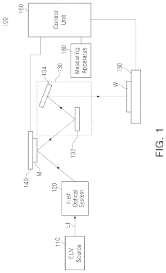
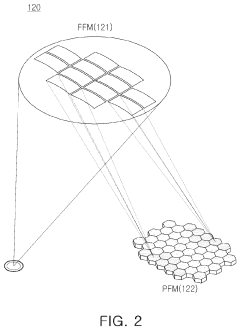
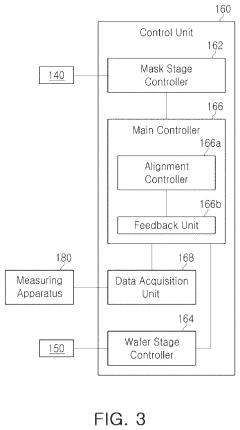
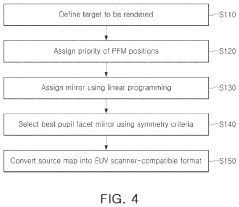
- The implementation of a freeform EUV illumination system using linear programming and priority optimization to assign mirror positions, allowing for the generation of an optimized illumination system that can be converted into a form recognizable by an EUV scanner, thereby improving patterning performance.
Regulatory Framework Impact on EUV Adoption
The regulatory landscape surrounding EUV lithography technology has evolved significantly over the past decade, creating a complex framework that both enables and constrains industry adoption. Export control regulations, particularly those implemented by the United States, European Union, and Japan, have established strict limitations on the transfer of EUV technology to certain countries, most notably China. These controls are primarily driven by national security concerns, as EUV lithography represents a critical technology for advanced semiconductor manufacturing with potential dual-use applications.
The International Traffic in Arms Regulations (ITAR) and Export Administration Regulations (EAR) in the United States have specifically targeted EUV lithography equipment, requiring special licenses for international sales. This regulatory environment has created significant market access barriers, effectively limiting the global distribution of ASML's EUV systems, the sole commercial provider of this technology.
Environmental and safety regulations also play a crucial role in EUV adoption. The technology utilizes tin droplets and powerful lasers to generate extreme ultraviolet light, creating potential workplace hazards that must be managed according to strict occupational safety standards. Additionally, the substantial energy consumption of EUV systems has drawn attention from environmental regulatory bodies, particularly in regions with aggressive carbon reduction targets.
Intellectual property regulations further complicate the EUV landscape. The technology represents a convergence of thousands of patents across optics, materials science, and precision engineering. Cross-licensing agreements and patent pools have become necessary to navigate this complex IP environment, with regulatory authorities in multiple jurisdictions monitoring potential anti-competitive practices in this highly concentrated market.
The semiconductor industry has responded to these regulatory challenges through various adaptation strategies. Companies have established dedicated compliance teams to navigate export controls, invested in environmental mitigation technologies to meet sustainability requirements, and developed sophisticated IP management approaches. Industry associations have also engaged in active dialogue with regulatory bodies to shape policies that balance security concerns with innovation needs.
Looking forward, the regulatory framework surrounding EUV lithography will likely continue to evolve as geopolitical tensions persist and environmental standards become more stringent. This dynamic regulatory environment will remain a critical factor influencing the pace and direction of EUV adoption across the global semiconductor industry.
Export Control and National Security Implications
The geopolitical landscape surrounding EUV lithography has become increasingly complex as nations recognize its strategic importance in semiconductor manufacturing. Export controls on EUV technology, particularly those implemented by the United States and its allies, have significantly shaped global adoption patterns. The U.S. has leveraged the International Traffic in Arms Regulations (ITAR) and Export Administration Regulations (EAR) to restrict the transfer of EUV technology to certain countries, most notably China. These restrictions have effectively created a technological divide, limiting China's access to advanced semiconductor manufacturing capabilities.
The Netherlands, home to ASML—the sole producer of commercial EUV lithography machines—has aligned with U.S. policies by implementing its own export restrictions. This coordination among Western allies demonstrates how EUV lithography has become entangled in broader national security considerations beyond purely commercial interests. The Dutch government's decision to restrict ASML from selling its most advanced EUV systems to China illustrates the prioritization of security alliances over potential market opportunities.
Japan and South Korea have similarly implemented export controls on semiconductor manufacturing equipment and materials, creating a multilateral regulatory framework that significantly impacts global EUV adoption. These coordinated restrictions have reinforced technological leadership among allied nations while potentially slowing global diffusion of the technology.
From a national security perspective, EUV lithography represents a dual-use technology with both commercial and military applications. Advanced semiconductors produced using EUV lithography are critical components in military systems, artificial intelligence applications, and cybersecurity infrastructure. Nations possessing EUV capabilities gain strategic advantages in both economic competitiveness and defense capabilities, explaining the intense focus on controlling this technology.
The regulatory environment has created distinct adoption trajectories for different regions. While companies in the U.S., Taiwan, South Korea, and Japan have accelerated EUV adoption with governmental support, Chinese manufacturers face significant barriers. This has prompted substantial investments in alternative technologies and domestic semiconductor equipment development in China, potentially leading to technological divergence in the semiconductor industry.
Looking forward, the regulatory landscape will likely continue evolving as geopolitical tensions fluctuate. Companies planning EUV adoption must navigate complex compliance requirements and anticipate potential regulatory changes that could impact technology access, supply chains, and market opportunities. The interplay between national security concerns and technological advancement will remain a defining factor in the global distribution and implementation of EUV lithography technology.
Unlock deeper insights with Patsnap Eureka Quick Research — get a full tech report to explore trends and direct your research. Try now!
Generate Your Research Report Instantly with AI Agent
Supercharge your innovation with Patsnap Eureka AI Agent Platform!