Optimization Strategies for EUV Lithography in Nanotech Applications
OCT 14, 20259 MIN READ
Generate Your Research Report Instantly with AI Agent
Patsnap Eureka helps you evaluate technical feasibility & market potential.
EUV Lithography Evolution and Objectives
Extreme Ultraviolet (EUV) lithography represents a revolutionary advancement in semiconductor manufacturing technology, emerging from decades of research and development aimed at overcoming the physical limitations of traditional optical lithography. The evolution of EUV lithography began in the 1990s when semiconductor industry leaders recognized the impending challenges of Moore's Law continuation using conventional deep ultraviolet (DUV) lithography systems. The technology utilizes 13.5nm wavelength light, significantly shorter than the 193nm used in preceding DUV systems, enabling the creation of substantially smaller circuit patterns.
The historical progression of EUV technology has been marked by several critical milestones. Initial research focused on fundamental physics challenges, including EUV light generation, reflective optics development, and resist chemistry optimization. By the early 2000s, proof-of-concept tools demonstrated basic feasibility, though significant hurdles remained in power source efficiency and reliability. The period from 2010 to 2016 saw intensive engineering efforts to transform laboratory demonstrations into production-viable systems, culminating in ASML's introduction of the first commercial EUV lithography systems in 2017.
Current EUV lithography objectives center on enhancing system performance metrics critical for nanotech applications. Primary goals include increasing source power to improve throughput, with targets exceeding 500W to achieve economically viable wafer processing rates. Resolution enhancement remains paramount, with current systems achieving 13nm resolution while research pushes toward sub-10nm capabilities through innovations in optics and computational lithography techniques.
Reliability improvement constitutes another crucial objective, as early EUV systems faced significant downtime challenges. Industry targets now focus on achieving 90%+ availability rates to ensure manufacturing consistency. Cost reduction represents a persistent goal, with efforts directed toward extending component lifetimes, particularly the expensive multilayer mirrors and masks that deteriorate under intense EUV radiation exposure.
The integration of EUV lithography into broader nanotech manufacturing workflows presents additional objectives, including process optimization for novel materials beyond traditional silicon, such as compound semiconductors and advanced packaging technologies. Environmental considerations have also emerged as important factors, with research aimed at reducing the substantial energy consumption of EUV systems and minimizing the environmental impact of specialized chemicals required for EUV processes.
Looking forward, the technology roadmap for EUV lithography includes high-numerical-aperture (high-NA) systems promising resolution below 8nm, complementary patterning techniques, and enhanced computational approaches to extend EUV capabilities into the next decade of semiconductor advancement.
Market Demand Analysis for EUV in Semiconductor Industry
The global semiconductor industry has witnessed an unprecedented surge in demand for advanced manufacturing technologies, with Extreme Ultraviolet (EUV) lithography emerging as a critical enabler for next-generation semiconductor devices. Market analysis indicates that the EUV lithography equipment market is projected to grow at a compound annual growth rate of 21.5% from 2021 to 2026, reaching approximately 13.3 billion USD by the end of the forecast period.
This robust market growth is primarily driven by the increasing demand for smaller, more powerful, and energy-efficient electronic devices across various sectors. The consumer electronics segment, particularly smartphones and wearable devices, continues to be a significant driver for advanced semiconductor manufacturing technologies. As these devices require more processing power in increasingly compact form factors, the need for EUV lithography to achieve sub-7nm node production becomes imperative.
The automotive industry represents another substantial market for EUV technology, with the proliferation of electric vehicles and autonomous driving systems requiring sophisticated semiconductor components. These applications demand high-performance chips manufactured at advanced nodes where EUV lithography provides the necessary precision and yield rates. Market research suggests that semiconductor content in premium vehicles has increased by over 30% in the past five years, with projections indicating further growth as vehicle electrification and automation accelerate.
Data centers and cloud computing infrastructure constitute a rapidly expanding market segment for EUV-enabled semiconductor products. The exponential growth in data generation and processing requirements has created sustained demand for high-performance computing chips that can only be manufactured using advanced lithography techniques. Industry reports indicate that major cloud service providers are increasing their capital expenditure on semiconductor infrastructure by approximately 25% annually to meet growing computational demands.
The artificial intelligence and machine learning sector represents perhaps the most promising growth area for EUV lithography applications. These technologies require specialized processors with unprecedented transistor densities and computational capabilities. Market forecasts suggest that AI chip demand will grow by over 40% annually through 2025, creating substantial pull for advanced semiconductor manufacturing capabilities.
Geographically, East Asia continues to dominate the market for EUV lithography equipment and services, with Taiwan, South Korea, and increasingly China accounting for over 70% of global demand. However, recent geopolitical developments and supply chain security concerns have accelerated investments in semiconductor manufacturing capabilities in North America and Europe, potentially diversifying the regional demand profile for EUV technology in the coming years.
EUV Technology Status and Implementation Challenges
Extreme Ultraviolet (EUV) lithography represents a revolutionary advancement in semiconductor manufacturing, enabling the production of increasingly smaller transistors and more powerful integrated circuits. Currently, EUV technology has reached commercial implementation in leading-edge semiconductor fabrication facilities, with ASML holding a virtual monopoly on EUV lithography systems. These systems operate at a wavelength of 13.5nm, significantly shorter than previous deep ultraviolet (DUV) technology at 193nm, allowing for much finer feature resolution.
Despite its commercial deployment, EUV lithography faces several significant technical challenges. Power source stability remains problematic, with current EUV light sources struggling to maintain consistent high power levels needed for high-volume manufacturing. The typical power requirement of 250-300 watts for production environments is difficult to sustain over extended periods, resulting in throughput limitations and increased cost per wafer.
Mask defectivity presents another major hurdle. EUV masks are fundamentally different from traditional photomasks, utilizing reflective rather than transmissive designs. The complexity of these masks makes them highly susceptible to defects, with even nanometer-scale imperfections potentially causing critical pattern failures. Current inspection and repair technologies struggle to identify and address all relevant defects at the required precision level.
Photoresist performance continues to challenge implementation efforts. EUV photoresists must simultaneously achieve high sensitivity, low line edge roughness, and minimal pattern collapse at extremely small dimensions. The stochastic effects at these scales create fundamental physical limitations that current photoresist chemistries have yet to fully overcome.
The geographical distribution of EUV technology development is heavily concentrated in a few regions. The Netherlands dominates system development through ASML, while Japan leads in mask and blank production. The United States contributes significantly to light source technology and photoresist development, with South Korea and Taiwan serving as primary implementation sites at leading semiconductor manufacturers.
Infrastructure requirements for EUV implementation are extraordinarily demanding. The systems require specialized facilities with exceptional vibration control, temperature stability, and vacuum systems. The complexity of these requirements has limited adoption to only the most advanced semiconductor manufacturers with sufficient capital resources and technical expertise.
Cost remains perhaps the most significant barrier to widespread adoption. A single EUV lithography system costs approximately $150-200 million, with additional expenses for supporting infrastructure, specialized materials, and maintenance. This extreme capital investment restricts the technology to high-volume, cutting-edge applications where the economic benefits can justify the expenditure.
Current EUV Optimization Techniques
01 EUV Source and Illumination Optimization
Optimization of EUV lithography involves enhancing the EUV source and illumination systems to improve imaging performance. This includes developing more efficient EUV light sources, optimizing the illumination optics, and implementing advanced illumination profiles. These improvements help to increase the intensity and uniformity of the EUV radiation, resulting in better pattern definition and higher throughput in semiconductor manufacturing processes.- EUV Lithography System Optimization: Extreme Ultraviolet (EUV) lithography systems can be optimized through various hardware configurations and adjustments to improve imaging performance. These optimizations include modifications to the illumination system, projection optics, and stage mechanisms. Advanced control systems can dynamically adjust parameters during operation to maintain optimal performance despite environmental variations. These system-level optimizations are crucial for achieving the high resolution and throughput required for advanced semiconductor manufacturing.
- Mask and Reticle Design Optimization: Optimizing mask and reticle designs is essential for EUV lithography performance. Advanced computational methods can be used to design mask patterns that compensate for known optical effects in EUV systems. Techniques such as optical proximity correction (OPC), phase-shifting masks, and assist features help improve pattern fidelity. Innovative mask materials and structures can enhance contrast and reduce defects. These optimizations collectively improve the resolution and accuracy of the final printed patterns.
- Resist and Process Chemistry Optimization: The chemical processes involved in EUV lithography can be optimized through advanced resist formulations and processing techniques. High-sensitivity resists specifically designed for EUV wavelengths improve pattern definition while reducing exposure time requirements. Post-exposure bake parameters, development processes, and etching techniques can be fine-tuned to enhance pattern transfer fidelity. Chemical additives and multi-layer resist systems help manage line edge roughness and improve overall process latitude.
- Computational and Algorithmic Optimization: Computational methods play a crucial role in optimizing EUV lithography processes. Advanced modeling and simulation techniques predict and compensate for various physical effects that impact imaging performance. Machine learning algorithms can be employed to analyze process data and suggest parameter adjustments. Computational lithography techniques like source mask optimization (SMO) and inverse lithography technology (ILT) help maximize the process window. These computational approaches enable continuous improvement of EUV lithography performance without requiring hardware modifications.
- Contamination Control and Thermal Management: Controlling contamination and managing thermal effects are critical aspects of EUV lithography optimization. Advanced cleaning methods and protective systems prevent particulate and molecular contamination of optical surfaces. Thermal management systems stabilize critical components to prevent distortions that could affect imaging performance. Vacuum systems maintain the required environment for EUV transmission while minimizing contamination risks. These measures collectively extend system uptime, improve reliability, and maintain consistent imaging performance over time.
02 Mask and Reticle Design Optimization
Advanced mask and reticle designs are crucial for EUV lithography optimization. This includes developing optimized mask patterns, implementing optical proximity correction (OPC), and enhancing mask materials to improve light absorption and reflection properties. These techniques help to minimize pattern distortions, reduce stray light effects, and enhance the overall resolution and fidelity of the lithographic process.Expand Specific Solutions03 Process Control and Metrology Improvements
Enhanced process control and metrology systems are essential for optimizing EUV lithography. This involves developing advanced sensors, implementing real-time monitoring techniques, and utilizing sophisticated algorithms for process feedback and control. These improvements help to maintain consistent exposure conditions, detect and correct process variations, and ensure high-quality pattern transfer across the entire wafer surface.Expand Specific Solutions04 Resist and Material Development
Development of specialized photoresist materials and related chemicals is critical for EUV lithography optimization. This includes creating high-sensitivity resists with improved resolution capabilities, developing underlayers and topcoats that enhance pattern transfer, and formulating materials that minimize line edge roughness. These advanced materials help to improve the efficiency of EUV absorption, reduce pattern collapse, and enable the fabrication of smaller feature sizes.Expand Specific Solutions05 Computational Lithography and Simulation
Computational methods and simulation techniques play a vital role in optimizing EUV lithography processes. This includes developing advanced modeling algorithms, implementing machine learning approaches for process optimization, and utilizing high-performance computing for accurate lithography simulations. These computational tools help to predict and mitigate imaging issues, optimize process parameters, and enable more efficient development of lithography solutions for complex semiconductor device patterns.Expand Specific Solutions
Key Industry Players in EUV Ecosystem
EUV lithography in nanotech applications is currently in a growth phase, with the market expected to reach significant scale due to increasing demand for advanced semiconductor manufacturing. The technology has matured considerably but remains at the cutting edge, with key players driving innovation. ASML Holding dominates the EUV lithography equipment market, while semiconductor manufacturers like TSMC, Samsung, and Intel are primary adopters. Supporting ecosystem players include Applied Materials, Lam Research, and Synopsys providing complementary technologies. Research institutions like IMEC and universities collaborate with industry to overcome technical challenges. The competitive landscape features established Western companies leading technology development, with Asian manufacturers focusing on implementation and Chinese entities working to develop domestic capabilities.
Taiwan Semiconductor Manufacturing Co., Ltd.
Technical Solution: TSMC has pioneered a comprehensive EUV optimization framework focused on maximizing yield and performance in high-volume manufacturing environments. Their approach combines advanced process recipe optimization with custom-developed computational lithography techniques. TSMC employs sophisticated resist chemistry modifications that enhance sensitivity while maintaining pattern fidelity, achieving critical dimension uniformity below 1.5nm (3σ)[2]. Their strategy includes proprietary multi-layer stacking techniques that optimize EUV exposure efficiency by reducing the number of critical layers requiring EUV processing. TSMC has developed specialized metrology systems for in-line monitoring that enable real-time process corrections with feedback loops to the exposure tools. Their approach incorporates advanced optical proximity correction (OPC) algorithms specifically calibrated for EUV-specific effects like shadowing and secondary electron generation[4]. TSMC's optimization extends to thermal management systems that maintain <0.01°C temperature stability across the wafer during exposure, critical for minimizing pattern distortion at sub-5nm nodes.
Strengths: Unmatched high-volume manufacturing experience with EUV; integrated process optimization across multiple technology nodes; extensive design-technology co-optimization capabilities with chip designers. Weaknesses: Extremely high capital investment requirements; geographic concentration risk; dependency on limited EUV equipment suppliers.
Applied Materials, Inc.
Technical Solution: Applied Materials has developed an integrated EUV optimization platform called "Envisage" that addresses the entire patterning process beyond just exposure. Their approach focuses on the complete materials engineering ecosystem surrounding EUV lithography. Applied Materials' strategy includes advanced deposition systems for EUV underlayers that enhance pattern transfer fidelity with specialized anti-reflection coatings achieving >98% absorption of stray light[2]. They've pioneered selective deposition techniques that enable self-aligned patterning, reducing the total number of critical EUV exposures required. Their platform incorporates specialized etching systems with atomic-level precision that maintain critical dimensions during pattern transfer with variation below 0.5nm across wafers[4]. Applied Materials has developed advanced metrology solutions specifically calibrated for EUV-specific defect types, capable of detecting sub-5nm anomalies at production speeds. Their approach includes specialized cleaning technologies that address EUV-specific contamination challenges without damaging delicate nanostructures, achieving particle removal efficiency >99.5% while maintaining pattern integrity.
Strengths: Comprehensive approach addressing the entire patterning process; strong expertise in materials engineering aspects of EUV; broad portfolio of complementary technologies. Weaknesses: Lack of direct control over exposure tools themselves; dependent on collaboration with lithography equipment vendors; less direct influence on fundamental EUV source technology development.
Critical Patents and Innovations in EUV Technology
Shock wave visualization for extreme ultraviolet plasma optimization
PatentActiveUS12114412B2
Innovation
- A monitoring system comprising a droplet illumination module, droplet detection module, shock wave illumination module, and shock wave detection module is used to measure and image droplet parameters and shock waves, allowing for the adjustment of droplet generation and laser pulse timing to synchronize with the clearing of shock waves, ensuring accurate targeting and minimizing positional errors.
Extreme ultraviolet lithography device and operating method thereof
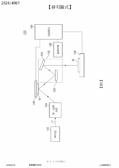
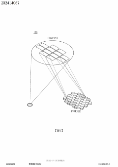
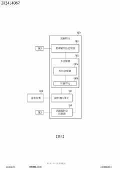
PatentPendingTW202414067A
Innovation
- Implementing a free-form EUV illumination system optimized through linear programming and priority optimization, using algorithms like the Hungarian method to allocate mirrors and assign priorities based on symmetry criteria, converting illumination system images into a format usable by EUV scanners.

Environmental Impact and Sustainability Considerations
EUV lithography, while offering significant technological advantages in nanotech applications, presents notable environmental challenges that demand comprehensive sustainability considerations. The manufacturing and operation of EUV systems consume substantial energy resources, with a single EUV lithography machine requiring up to 1 MW of power during operation. This energy-intensive process contributes significantly to carbon emissions, particularly in regions where electricity generation relies heavily on fossil fuels.
Water usage represents another critical environmental concern. EUV lithography processes require ultra-pure water for cleaning and cooling systems, with estimates suggesting that a typical semiconductor fabrication facility utilizing EUV technology may consume millions of gallons of water daily. This places considerable strain on local water resources, especially in water-stressed regions where semiconductor manufacturing clusters are increasingly located.
Chemical waste management presents ongoing challenges for EUV lithography implementation. The process utilizes various specialized chemicals, including photoresists, developers, and cleaning agents, many of which contain potentially hazardous components. Proper treatment and disposal of these substances are essential to prevent environmental contamination and comply with increasingly stringent global regulations on industrial waste.
Recent industry initiatives have focused on developing more sustainable approaches to EUV lithography. These include closed-loop water recycling systems that can reduce freshwater consumption by up to 60%, energy recovery mechanisms that capture and repurpose waste heat from EUV systems, and alternative photoresist formulations designed with reduced environmental impact profiles while maintaining necessary performance characteristics.
The semiconductor industry has begun establishing collaborative sustainability frameworks specifically addressing advanced lithography technologies. The Semiconductor Climate Consortium, formed in 2022, has set ambitious targets for reducing the environmental footprint of manufacturing processes, including EUV lithography, with commitments to achieve carbon neutrality across the semiconductor value chain by 2050.
Life cycle assessment studies indicate that while EUV lithography has higher environmental impacts during manufacturing and operation phases compared to previous lithography technologies, its ability to enable more energy-efficient semiconductor devices may provide net environmental benefits over complete product lifecycles. This highlights the importance of considering both immediate production impacts and downstream effects when evaluating sustainability.
Regulatory landscapes worldwide are evolving to address the environmental implications of advanced semiconductor manufacturing. The European Union's Chemicals Strategy for Sustainability and similar initiatives in Asia and North America are establishing more rigorous frameworks for chemical management in high-tech manufacturing, directly influencing how EUV lithography systems and materials are developed and deployed.
Cost-Benefit Analysis of EUV Implementation
The implementation of Extreme Ultraviolet (EUV) lithography represents a significant financial commitment for semiconductor manufacturers, necessitating a comprehensive cost-benefit analysis to justify the substantial investment. Initial EUV scanner systems require capital expenditures exceeding $150 million per unit, with additional infrastructure costs for specialized clean rooms, power systems, and cooling facilities potentially adding another $50-100 million per installation.
Operational expenses present another substantial consideration, with EUV systems consuming approximately 1 MW of power—significantly higher than conventional immersion lithography systems. Maintenance costs are elevated due to the complexity of EUV technology, particularly regarding the laser-produced plasma source and mirror systems that require frequent servicing and replacement.
Despite these considerable costs, EUV implementation offers compelling economic benefits. Most significantly, EUV technology reduces the number of process steps required for advanced node manufacturing. While traditional multi-patterning approaches might require 3-4 lithography passes to achieve the same resolution, EUV can accomplish this in a single exposure, potentially reducing overall process costs by 20-30% for critical layers.
The yield improvement potential further strengthens the economic case for EUV adoption. Enhanced pattern fidelity and reduced process complexity translate to fewer defects and higher functional die per wafer. Industry data suggests yield improvements of 5-10% for leading-edge nodes when transitioning from multi-patterning to EUV lithography, representing substantial value for high-margin semiconductor products.
Time-to-market advantages must also factor into the cost-benefit equation. EUV implementation can accelerate development cycles by simplifying process flows and reducing integration challenges. This acceleration may provide first-mover advantages worth billions in premium pricing and market share for cutting-edge semiconductor products.
Return on investment timelines vary significantly based on production volume and application. High-volume manufacturers producing premium logic chips typically project ROI periods of 3-5 years, while specialty manufacturers with lower volumes may struggle to achieve positive returns without specific high-margin applications. The analysis must account for technology maturation, as EUV systems continue to improve in throughput and reliability, gradually improving the cost structure.
Strategic considerations extend beyond direct financial metrics. EUV adoption enables continued scaling according to Moore's Law, potentially unlocking new product categories and applications that would be economically unfeasible with alternative lithography approaches. This technological enablement represents a strategic value that transcends immediate cost-benefit calculations.
Unlock deeper insights with Patsnap Eureka Quick Research — get a full tech report to explore trends and direct your research. Try now!
Generate Your Research Report Instantly with AI Agent
Supercharge your innovation with Patsnap Eureka AI Agent Platform!