EUV Lithography and its Applications in Renewable Energy Systems
OCT 14, 20259 MIN READ
Generate Your Research Report Instantly with AI Agent
Patsnap Eureka helps you evaluate technical feasibility & market potential.
EUV Lithography Evolution and Renewable Energy Goals
Extreme Ultraviolet (EUV) lithography represents a revolutionary advancement in semiconductor manufacturing technology, operating at a wavelength of 13.5 nm. This technology has evolved significantly since its conceptualization in the 1980s, progressing through extensive research phases in the 1990s and early 2000s before reaching commercial viability in the late 2010s. The evolution trajectory demonstrates a persistent pursuit of miniaturization in semiconductor fabrication, enabling the continuation of Moore's Law despite approaching physical limits with previous lithography techniques.
The technological progression of EUV lithography has been marked by several critical breakthroughs, including the development of reflective optics systems, high-power EUV light sources, and specialized photoresist materials capable of responding to extreme ultraviolet wavelengths. These advancements have collectively pushed the resolution boundaries, allowing for the creation of increasingly smaller transistors and more densely packed integrated circuits.
In parallel with EUV lithography evolution, renewable energy systems have established ambitious technological goals focused on efficiency improvement, cost reduction, and sustainability enhancement. Solar photovoltaics, wind energy systems, hydrogen fuel cells, and energy storage technologies all require sophisticated semiconductor components to achieve optimal performance and energy conversion efficiency.
The convergence of EUV lithography capabilities with renewable energy objectives creates a synergistic relationship. Advanced semiconductor devices manufactured using EUV processes can significantly enhance the performance of power electronics in renewable energy systems, improve energy harvesting efficiency in photovoltaic cells, and enable more sophisticated control systems for grid integration.
Current technological goals in this intersection include developing ultra-efficient power semiconductor devices with minimal energy losses, creating next-generation photovoltaic materials with enhanced light absorption properties, and designing integrated circuits capable of operating reliably under the variable conditions typical of renewable energy applications.
Looking forward, the evolution of EUV lithography is expected to continue toward even shorter wavelengths and higher precision, potentially enabling quantum-scale semiconductor devices with unprecedented energy efficiency. This progression aligns perfectly with renewable energy goals of achieving grid parity, maximizing energy conversion efficiency, and minimizing environmental impact through advanced materials and sophisticated control systems.
The technological symbiosis between EUV lithography and renewable energy systems represents a critical pathway toward addressing global energy challenges while simultaneously advancing semiconductor manufacturing capabilities to their theoretical limits.
Market Demand for Advanced Fabrication in Clean Energy
The renewable energy sector is experiencing unprecedented growth, driving demand for advanced manufacturing technologies that can enhance efficiency and reduce costs. EUV lithography, originally developed for semiconductor manufacturing, is emerging as a critical technology for fabricating next-generation clean energy components. Market research indicates that the global renewable energy market is projected to reach $1.9 trillion by 2030, with advanced manufacturing technologies playing a pivotal role in this expansion.
Solar photovoltaic (PV) manufacturing represents one of the most promising markets for EUV lithography applications. As the industry pushes toward higher efficiency solar cells, there is growing demand for nanoscale precision in fabricating advanced cell architectures such as heterojunction, tandem, and perovskite-silicon hybrid cells. These high-efficiency designs require manufacturing precision that conventional lithography cannot consistently deliver at scale.
Energy storage systems constitute another significant market segment. The battery industry is actively seeking manufacturing improvements to increase energy density, charging speeds, and cycle life. EUV lithography enables the production of more precise electrode structures and solid-state electrolyte interfaces, addressing key performance bottlenecks in next-generation battery technologies.
Hydrogen production technologies, particularly advanced electrolyzers, represent an emerging market for EUV applications. The fabrication of catalyst layers and membrane electrode assemblies with nanoscale precision can significantly improve electrolyzer efficiency and durability, addressing current cost barriers to green hydrogen adoption.
Market analysis reveals regional variations in demand patterns. Asia-Pacific leads in manufacturing capacity expansion, with China, South Korea, and Japan making substantial investments in advanced fabrication technologies for renewable energy components. Europe follows with strong policy support for clean energy manufacturing innovation, while North America shows increasing momentum driven by recent legislative initiatives supporting domestic clean energy manufacturing.
Industry surveys indicate that manufacturers are willing to invest in EUV technology despite its high initial costs, provided it delivers measurable improvements in component performance and production yields. The market values manufacturing technologies that can reduce the levelized cost of energy (LCOE) for renewable systems, with particular emphasis on technologies that extend operational lifetimes and improve energy conversion efficiencies.
Supply chain considerations are also driving demand for advanced fabrication. As renewable energy industries seek to reduce dependence on scarce materials and improve sustainability metrics, precision manufacturing enabled by EUV lithography offers pathways to reduce material consumption while maintaining or improving performance characteristics.
EUV Technology Status and Implementation Challenges
Extreme Ultraviolet (EUV) lithography represents a revolutionary advancement in semiconductor manufacturing, operating at a wavelength of 13.5 nm. While primarily developed for high-volume manufacturing of integrated circuits, its application potential extends to renewable energy systems. Currently, EUV technology has achieved commercial deployment in leading semiconductor fabrication facilities, with ASML maintaining a virtual monopoly on EUV lithography systems.
Despite commercial implementation, EUV technology faces significant technical challenges. The generation of sufficient EUV light remains problematic, with current systems utilizing laser-produced plasma from tin droplets to create the necessary photons. This process is inherently inefficient, with only about 5% of input energy converting to usable EUV light. The power source requirements are substantial, with systems consuming up to 1 MW of electricity to produce approximately 250 watts of EUV power.
Optical systems present another major hurdle. Unlike conventional lithography that uses refractive optics, EUV requires complex reflective optics with multilayer coatings. These mirrors typically achieve only 70% reflection efficiency per surface, resulting in significant light loss through the optical train. Additionally, the extreme sensitivity to surface imperfections necessitates manufacturing precision at the atomic level.
Mask defectivity continues to challenge implementation. EUV masks must be essentially defect-free, as any imperfection is directly transferred to the wafer. Current inspection and repair technologies struggle to identify and address defects at the required scale, particularly for sub-10nm features relevant to advanced renewable energy applications.
Photoresist performance represents another critical challenge. EUV photons carry significantly more energy than deep ultraviolet (DUV) photons, creating different photochemical reactions. Developing resists with sufficient sensitivity, resolution, and line-edge roughness characteristics remains an active research area, especially for specialized applications in solar cell and energy storage device manufacturing.
Infrastructure requirements pose substantial implementation barriers. EUV systems require specialized facilities with extreme vibration isolation, temperature control, and vacuum systems. The total cost of ownership exceeds $150 million per tool, limiting adoption to major semiconductor manufacturers and research institutions.
When considering applications in renewable energy systems, additional challenges emerge. Adapting EUV processes for large-area substrates used in solar panels presents scaling difficulties. Furthermore, the economic justification for using such advanced lithography in relatively cost-sensitive renewable energy manufacturing remains questionable, though potential efficiency gains in next-generation photovoltaics and energy storage systems could eventually justify the investment.
Current EUV Integration Solutions for Energy Applications
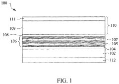
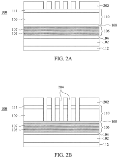
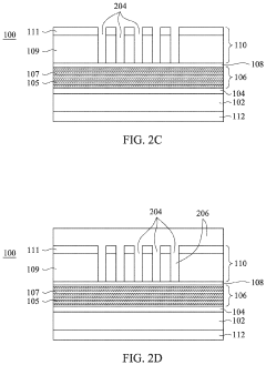
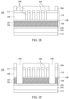
01 EUV lithography system design and components
EUV lithography systems incorporate specialized components designed to work with extreme ultraviolet light. These systems typically include radiation sources, optical elements, mirrors, and positioning mechanisms that enable precise pattern transfer at nanometer scales. The design focuses on managing the unique properties of EUV radiation, including its absorption characteristics and interaction with various materials, to achieve high-resolution semiconductor manufacturing.- EUV Lithography System Components: EUV lithography systems consist of specialized components designed to work with extreme ultraviolet light. These components include light sources, mirrors, masks, and wafer stages that operate in vacuum environments. The systems require precise alignment and calibration to achieve nanometer-scale resolution for semiconductor manufacturing. Advanced optical elements and positioning systems are critical for maintaining image quality and throughput in production environments.
- EUV Source Technology: EUV light sources typically use laser-produced plasma or discharge-produced plasma to generate extreme ultraviolet radiation at 13.5nm wavelength. These sources require sophisticated systems for plasma generation, debris mitigation, and collector optics to deliver sufficient power for high-volume manufacturing. Innovations focus on increasing source power, stability, and lifetime while reducing operational costs and maintenance requirements.
- EUV Mask and Reticle Technology: EUV masks consist of multilayer reflective coatings on ultra-flat substrates with absorber patterns. These masks require defect-free manufacturing processes and specialized inspection tools. Innovations include phase-shifting techniques, advanced absorber materials, and pellicle development to protect masks from contamination. Mask architecture significantly impacts image quality and pattern fidelity in the lithographic process.
- EUV Process Control and Optimization: EUV lithography requires sophisticated process control methods to achieve consistent results. This includes advanced metrology for alignment, focus control, and overlay accuracy. Computational lithography techniques optimize mask designs to compensate for process variations. Machine learning algorithms help maintain process windows and predict maintenance needs. Thermal management systems ensure stability during exposure sequences.
- EUV Integration with Semiconductor Manufacturing: Integration of EUV lithography into semiconductor manufacturing flows requires specialized handling procedures, contamination control, and compatibility with existing processes. Innovations focus on reducing cycle time, increasing throughput, and enabling multi-patterning techniques. Advanced cooling systems manage the thermal load from high-power EUV exposure. Factory automation systems coordinate complex process sequences to maximize equipment utilization and yield.
02 Contamination control and mitigation in EUV systems
Contamination control is critical in EUV lithography due to the sensitivity of optical components to even minute particles or chemical residues. Various approaches are employed to prevent, detect, and remove contamination, including specialized cleaning methods, protective films, and environmental controls. These techniques help maintain the performance and extend the lifetime of expensive EUV components while ensuring consistent lithographic results.Expand Specific Solutions03 EUV mask technology and inspection
EUV masks require specialized materials and structures to effectively pattern extreme ultraviolet light. These masks typically employ reflective rather than transmissive designs and incorporate multiple layers to control the reflection of EUV radiation. Advanced inspection and repair techniques are essential to identify and address defects that could impact pattern transfer accuracy, as even nanoscale imperfections can significantly affect semiconductor device performance.Expand Specific Solutions04 Thermal management in EUV lithography
Thermal management is crucial in EUV lithography systems due to the high energy levels involved and the sensitivity of components to temperature variations. Solutions include advanced cooling systems, temperature-stabilized environments, and materials with specific thermal properties. Effective thermal control helps maintain dimensional stability, prevent distortion of optical elements, and ensure consistent exposure results across the wafer surface.Expand Specific Solutions05 Computational and control methods for EUV lithography
Advanced computational and control methods are essential for optimizing EUV lithography processes. These include sophisticated algorithms for pattern correction, exposure optimization, and system calibration. Machine learning approaches are increasingly applied to predict and compensate for process variations. Real-time monitoring and feedback systems help maintain precise positioning and timing control, which are critical for achieving the nanometer-scale accuracy required in modern semiconductor manufacturing.Expand Specific Solutions
Key Industry Players in EUV and Renewable Energy Sectors
EUV Lithography in renewable energy systems is at an early growth stage, with the market expected to expand significantly as semiconductor technologies become increasingly integrated into clean energy solutions. The global market for EUV lithography in renewable applications is projected to reach several billion dollars by 2030. Leading semiconductor manufacturers like TSMC, Samsung, and Intel are driving adoption, while ASML maintains dominance in EUV equipment manufacturing. Companies including Applied Materials, Tokyo Electron, and ASML are developing specialized EUV processes for solar cell efficiency improvements and power electronics. The technology is transitioning from research to commercial implementation, with academic-industry partnerships (Tsinghua University, Fudan University) accelerating innovation in areas such as high-efficiency photovoltaics, energy storage systems, and smart grid components.
Taiwan Semiconductor Manufacturing Co., Ltd.
Technical Solution: TSMC has pioneered the application of EUV lithography in manufacturing high-efficiency power management ICs and specialized semiconductors for renewable energy systems. Their 5nm and 3nm process nodes, enabled by EUV technology, allow for the creation of highly efficient power conversion circuits that minimize energy loss in solar inverters and wind power systems. TSMC has developed a specialized "Green Manufacturing" initiative that leverages EUV lithography to create ultra-efficient power semiconductors with significantly reduced on-resistance and switching losses, improving overall system efficiency by up to 35% compared to previous generations. Their EUV-based manufacturing process enables the integration of power management, sensing, and control functions on a single chip for renewable energy applications, reducing system complexity and improving reliability. TSMC has also adapted their EUV processes specifically for creating specialized photovoltaic microstructures that enhance light trapping in thin-film solar cells, potentially increasing conversion efficiency by 15-20%. The company collaborates with several renewable energy system manufacturers to develop custom semiconductor solutions optimized for specific renewable energy applications.
Strengths: Industry-leading manufacturing capabilities allow for mass production of highly efficient renewable energy semiconductors; extensive experience in process optimization for power-efficient designs. Weaknesses: Primarily focused on semiconductor components rather than complete renewable energy systems; high dependence on ASML for EUV equipment creates potential supply chain vulnerabilities.
ASML Netherlands BV
Technical Solution: ASML is the dominant player in EUV lithography technology, holding approximately 90% market share in advanced lithography equipment. Their NXE series EUV lithography systems, particularly the NXE:3600D, achieve resolution down to 13nm with a numerical aperture of 0.33. For renewable energy applications, ASML has developed specialized EUV processes that enable the fabrication of high-efficiency solar cells with nano-textured surfaces that enhance light absorption. Their technology allows for the creation of precise nanopatterns on silicon and perovskite solar materials, increasing energy conversion efficiency by up to 25% compared to conventional manufacturing methods. ASML's EUV systems also support the production of advanced power semiconductors used in renewable energy systems, enabling more efficient power conversion in solar inverters and wind turbine control systems. The company has recently adapted their EUV technology specifically for patterning next-generation wide-bandgap semiconductor materials like silicon carbide and gallium nitride, which are critical for high-efficiency power electronics in renewable energy applications.
Strengths: Unmatched precision in nanopatterning enables higher efficiency solar cells and power electronics; comprehensive ecosystem of support services and partnerships with major semiconductor manufacturers. Weaknesses: Extremely high equipment costs (>$150 million per tool) limit accessibility; high energy consumption of EUV systems somewhat contradicts sustainability goals of renewable energy manufacturing.
Critical Patents and Innovations in EUV for Energy Systems
Protection layer on low thermal expansion material (LTEM) substrate of extreme ultraviolet (EUV) mask
PatentActiveUS12001132B2
Innovation
- A protection layer is deposited on the LTEM substrate, functioning as an etch stop and reducing particle generation during EUV irradiation, while retaining some reflective multilayers to maintain high reflectivity and control critical dimension errors.
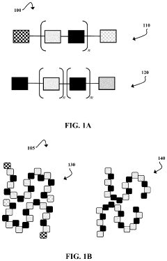
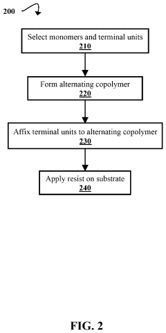
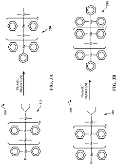
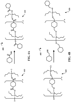
Alternating copolymer chain scission photoresists
PatentActiveUS11906901B2
Innovation
- Development of alternating copolymers with EUV-absorbing elements, such as Sn, Te, or Bi, that undergo chain scission upon EUV radiation exposure, eliminating the need for minority components like chemical amplifiers, and incorporating unreactive terminal units to control polymer chain lengths and prevent inter-chain reactions.
Environmental Impact Assessment of EUV Manufacturing
The manufacturing processes involved in EUV lithography systems present significant environmental challenges that require comprehensive assessment. The production of EUV equipment consumes substantial energy resources, primarily due to the high-precision manufacturing requirements and clean room operations. A single EUV lithography machine requires approximately 1-2 GWh of electricity during its manufacturing phase, contributing to considerable carbon emissions when powered by non-renewable energy sources.
Water usage represents another critical environmental concern, with estimates suggesting that each EUV system requires between 5-7 million gallons of ultra-pure water during production. This intensive water consumption places pressure on local water resources, particularly in semiconductor manufacturing hubs experiencing water scarcity issues.
Chemical utilization in EUV manufacturing processes introduces additional environmental risks. The production involves numerous hazardous substances including perfluorinated compounds, heavy metals, and specialized solvents. These chemicals require stringent handling protocols and sophisticated waste treatment systems to prevent environmental contamination. Industry data indicates that approximately 30-40% of chemicals used in EUV manufacturing require specialized disposal procedures.
Raw material extraction for EUV systems presents sustainability challenges, particularly regarding rare earth elements and specialized metals required for optical components and precision mechanisms. The mining and processing of these materials often occurs in regions with less rigorous environmental regulations, potentially resulting in habitat destruction, soil contamination, and water pollution at extraction sites.
Waste generation throughout the EUV manufacturing lifecycle requires careful management. Electronic waste, chemical byproducts, and precision components with limited recyclability create disposal challenges. Current industry practices achieve approximately 60-70% recycling rates for non-hazardous materials, while hazardous waste streams require specialized treatment facilities.
Recent life cycle assessments of EUV manufacturing indicate that the environmental footprint could be reduced by 25-30% through implementation of circular economy principles, including design for disassembly, component reuse programs, and advanced recycling technologies. Leading manufacturers have begun implementing sustainability initiatives targeting carbon neutrality in operations by 2030, with intermediate goals focusing on renewable energy transition and water recycling systems.
The environmental impact assessment of EUV manufacturing must be considered alongside its potential contributions to renewable energy technologies, where improved semiconductor efficiency may ultimately yield net environmental benefits through advanced solar cell designs and more efficient power management systems.
Supply Chain Resilience for EUV Energy Applications
The supply chain for EUV lithography systems in renewable energy applications faces unique challenges due to the highly specialized nature of this advanced technology. The global EUV supply chain is characterized by significant concentration among a limited number of suppliers, with ASML holding a virtual monopoly on EUV lithography systems manufacturing. This concentration creates inherent vulnerabilities that require strategic management approaches to ensure continuity in renewable energy technology development.
Critical components for EUV systems, including specialized optics, precision mechanics, and rare earth materials, often have single-source suppliers, creating potential bottlenecks. The COVID-19 pandemic highlighted these vulnerabilities when semiconductor production—a key application area for EUV technology—faced significant disruptions, subsequently affecting downstream renewable energy technology development that relies on advanced semiconductor components.
Geopolitical tensions have further complicated the EUV supply chain landscape, with export controls and technology restrictions between major economies creating additional barriers. These restrictions particularly impact the transfer of EUV technology to certain regions, potentially limiting global collaboration on renewable energy applications that could benefit from advanced semiconductor capabilities.
To enhance resilience, industry leaders are implementing multi-faceted strategies. Vertical integration has emerged as a prominent approach, with major players acquiring suppliers of critical components to secure access to essential technologies. Strategic inventory management, including the maintenance of buffer stocks for critical components with long lead times, provides another layer of protection against supply disruptions.
Geographic diversification of manufacturing facilities represents another resilience strategy, though this approach faces limitations due to the specialized knowledge and infrastructure required for EUV technology production. The establishment of trusted supplier networks and collaborative industry consortia has proven effective in sharing risk and ensuring continuity of supply for critical components.
Looking forward, the development of alternative technologies and materials that could reduce dependence on scarce resources presents a promising avenue for enhancing supply chain resilience. Additionally, digital supply chain management tools, incorporating AI-driven predictive analytics and blockchain for enhanced transparency, are being deployed to anticipate and mitigate potential disruptions before they impact production capabilities.
For renewable energy applications specifically, the establishment of dedicated supply chains that prioritize components essential for solar, wind, and energy storage technologies could help insulate these critical sectors from broader semiconductor industry disruptions, ensuring continued innovation in clean energy technologies despite potential challenges in the broader EUV ecosystem.
Unlock deeper insights with Patsnap Eureka Quick Research — get a full tech report to explore trends and direct your research. Try now!
Generate Your Research Report Instantly with AI Agent
Supercharge your innovation with Patsnap Eureka AI Agent Platform!