

Understanding How EUV Lithography Impacts Market Dynamics
OCT 14, 20259 MIN READ
Generate Your Research Report Instantly with AI Agent
PatSnap Eureka helps you evaluate technical feasibility & market potential.
EUV Lithography Evolution and Objectives
Extreme Ultraviolet (EUV) lithography represents a revolutionary advancement in semiconductor manufacturing, marking a significant departure from traditional Deep Ultraviolet (DUV) lithography techniques. The evolution of EUV technology spans over three decades, beginning in the 1980s with initial research into short-wavelength lithography solutions. By utilizing 13.5nm wavelength light, EUV enables the production of semiconductor chips with feature sizes below 7nm, addressing the limitations of previous lithography methods that struggled to keep pace with Moore's Law.
The development trajectory of EUV lithography has been characterized by persistent technical challenges and substantial industry collaboration. Early research focused primarily on light source development, with significant breakthroughs occurring in the early 2000s when ASML partnered with Cymer to develop commercially viable EUV light sources. The period between 2010 and 2018 saw intensive refinement of the technology, culminating in the introduction of production-ready EUV lithography systems.
Current EUV lithography objectives center on enhancing throughput capabilities, improving resolution limits, and reducing overall cost of ownership. The industry aims to achieve stable production at 3nm nodes and below, with particular emphasis on increasing wafer throughput from current levels of approximately 125-150 wafers per hour to over 200 wafers per hour. Additionally, there are concerted efforts to extend EUV technology through high-NA (numerical aperture) systems, which promise to enable feature sizes approaching 1nm.
The technological roadmap for EUV lithography indicates a clear progression toward more sophisticated implementations. Near-term objectives include perfecting single-patterning techniques at the 5nm node, while medium-term goals focus on implementing EUV multi-patterning strategies for 3nm production. Long-term industry aspirations involve the successful deployment of high-NA EUV systems, potentially enabling semiconductor manufacturing at the angstrom scale.
From a market perspective, EUV lithography represents both a technological imperative and a strategic inflection point. The technology has created significant barriers to entry in advanced semiconductor manufacturing, effectively consolidating market power among a select group of companies capable of implementing EUV processes. The primary objective for industry stakeholders is to leverage EUV capabilities to maintain technological leadership while managing the substantial capital investments required for implementation.
The evolution of EUV lithography continues to be shaped by the fundamental tension between technical possibility and economic viability. As the technology matures, objectives increasingly focus on optimizing the balance between performance enhancements and cost considerations, particularly as the industry contemplates the transition to high-NA EUV systems and beyond.
Semiconductor Industry Market Demand Analysis
The semiconductor industry is experiencing unprecedented demand growth driven by multiple technological waves converging simultaneously. The global semiconductor market reached $556 billion in 2021 and is projected to exceed $1 trillion by 2030, representing a compound annual growth rate of approximately 7%. This growth trajectory is primarily fueled by the expansion of artificial intelligence applications, 5G infrastructure deployment, autonomous vehicles, and the proliferation of IoT devices across consumer and industrial sectors.
EUV lithography has become a critical enabler for this market expansion by allowing manufacturers to continue Moore's Law progression into sub-7nm nodes. Market analysis indicates that demand for chips manufactured using EUV technology is growing at nearly twice the rate of the broader semiconductor market, highlighting the premium value placed on cutting-edge process technologies.
The geographic distribution of semiconductor demand is undergoing significant shifts. While North America remains the largest consumer of advanced semiconductors produced using EUV lithography (accounting for 24% of global demand), Asia-Pacific represents the fastest-growing market segment with 11% year-over-year growth. This regional demand pattern is reshaping supply chain strategies and manufacturing capacity investments globally.
By application segment, data centers and high-performance computing currently represent the largest demand driver for EUV-enabled chips, consuming approximately 31% of production. Mobile devices follow at 27%, with automotive applications showing the most dramatic growth trajectory as advanced driver-assistance systems and autonomous driving capabilities require increasingly sophisticated semiconductor components.
The introduction of EUV lithography has created distinct market segmentation between leading-edge and trailing-edge semiconductor products. This bifurcation is reflected in pricing structures, with EUV-produced chips commanding premium prices that are 40-60% higher than comparable previous-generation products. This price differential is expected to persist for at least 3-5 years until EUV capacity expansion reaches maturity.
Customer requirements are evolving in response to EUV capabilities. System integrators and OEMs are redesigning products to take advantage of the higher transistor densities, improved power efficiency, and enhanced performance characteristics enabled by EUV lithography. This is creating cascading demand effects throughout the semiconductor value chain, from design software to specialized materials and advanced packaging solutions.
Long-term market forecasts suggest that EUV lithography will remain a critical differentiator in the semiconductor industry through at least 2035, with multiple generations of the technology expected to support nodes down to 1nm and potentially beyond.
EUV Technology Status and Implementation Barriers
Extreme Ultraviolet (EUV) lithography represents a significant technological breakthrough in semiconductor manufacturing, currently deployed primarily in advanced nodes below 7nm. Despite its commercial implementation by leading manufacturers like TSMC, Samsung, and Intel, EUV technology faces substantial barriers that impact broader market adoption and dynamics.
The most significant implementation challenge remains the extraordinary cost structure associated with EUV systems. Each ASML EUV lithography machine costs approximately $150-200 million, with additional infrastructure requirements pushing total implementation costs beyond $300 million per unit. This creates a substantial entry barrier, effectively limiting adoption to only the largest semiconductor manufacturers with sufficient capital resources.
Technical challenges continue to constrain EUV's full potential. Power source stability remains problematic, with current EUV light sources achieving only 250-300 watts of power, below the ideal 500 watts needed for optimal throughput. This limitation directly impacts production efficiency and cost-effectiveness, particularly for high-volume manufacturing scenarios.
Mask defectivity presents another critical barrier. The complexity of EUV masks and the absence of pellicles in early implementations resulted in higher defect rates. While pellicle technology has improved, achieving and maintaining zero-defect production environments remains challenging, affecting yield rates and overall manufacturing economics.
Material science limitations further complicate implementation. Photoresist materials designed for EUV wavelengths (13.5nm) must balance sensitivity, resolution, and line-edge roughness—a complex trilemma that continues to challenge chemical suppliers and affects production quality and consistency.
From a supply chain perspective, ASML's monopoly on EUV systems creates significant vulnerability. The company's production capacity of approximately 35-40 systems annually cannot meet global demand, resulting in extended lead times of 12-18 months. This bottleneck restricts technology diffusion and reinforces market concentration among early adopters.
Workforce expertise represents an often-overlooked barrier. The specialized knowledge required to operate and maintain EUV systems necessitates substantial investment in human capital development. The limited pool of qualified engineers and technicians creates competition for talent and further concentrates capabilities among established players.
Geopolitical factors have emerged as a significant implementation barrier, with export controls and technology restrictions creating uneven access to EUV technology globally. These restrictions reshape supply chains and influence strategic decisions about manufacturing locations and technology investments, further complicating market dynamics and technology diffusion patterns.
Current EUV Implementation Strategies
01 EUV Lithography Equipment and Systems
Extreme Ultraviolet (EUV) lithography equipment and systems represent the cutting-edge technology in semiconductor manufacturing. These systems use short wavelength light to create extremely fine patterns on silicon wafers, enabling the production of smaller and more powerful microchips. The equipment includes sophisticated optical systems, light sources, and precision control mechanisms that work together to achieve nanometer-scale resolution. Advancements in these systems continue to drive the miniaturization of semiconductor devices and support the continuation of Moore's Law.- EUV Lithography Equipment and Systems: Extreme Ultraviolet (EUV) lithography equipment and systems represent the cutting-edge technology in semiconductor manufacturing. These systems use short wavelength light to create extremely fine patterns on silicon wafers, enabling the production of smaller and more powerful microchips. The equipment includes specialized light sources, mirrors, masks, and positioning systems designed to work with EUV wavelengths. Advancements in these systems have led to improved resolution, throughput, and reliability, driving the continued miniaturization of semiconductor devices.
- EUV Source Technology: EUV source technology is a critical component of EUV lithography systems, generating the extreme ultraviolet light needed for the lithographic process. These sources typically use laser-produced plasma or discharge-produced plasma to create EUV radiation. Innovations in this area focus on increasing source power, stability, and reliability while reducing debris generation and extending component lifetimes. Advancements in EUV source technology directly impact the economic viability and performance capabilities of EUV lithography in high-volume manufacturing environments.
- EUV Mask and Reticle Technology: EUV mask and reticle technology involves the development of specialized reflective masks that contain the circuit patterns to be transferred onto silicon wafers. Unlike traditional photomasks, EUV masks operate by reflection rather than transmission and require complex multilayer coatings to efficiently reflect EUV radiation. Innovations in this field address challenges such as defect detection and repair, pattern accuracy, and mask lifetime. Advanced inspection tools and manufacturing processes are essential for producing the defect-free masks required for high-yield semiconductor production.
- EUV Process Integration and Manufacturing: EUV process integration and manufacturing focuses on incorporating EUV lithography into semiconductor production workflows. This includes developing resist materials optimized for EUV exposure, establishing process control methods, and integrating EUV with other manufacturing steps. Challenges in this area include managing line-edge roughness, pattern collapse, and stochastic effects that become more pronounced at extreme dimensions. Innovations aim to improve yield, reduce defects, and enhance the overall efficiency of EUV-based semiconductor manufacturing processes.
- EUV Market and Economic Considerations: The EUV lithography market is characterized by significant capital investment requirements, complex supply chains, and strategic industry partnerships. Economic considerations include the cost of ownership, return on investment timelines, and competitive positioning among semiconductor manufacturers. The market dynamics are influenced by factors such as chip demand trends, technological roadmaps, and geopolitical considerations affecting the semiconductor industry. Analysis of these factors helps stakeholders make informed decisions about EUV technology adoption and investment strategies in the highly competitive semiconductor manufacturing landscape.
02 EUV Source Technology
EUV source technology is a critical component of EUV lithography systems, generating the extreme ultraviolet light needed for the lithographic process. These sources typically use laser-produced plasma or discharge-produced plasma to generate EUV radiation at a wavelength of 13.5 nm. Innovations in this area focus on increasing source power, stability, and reliability while reducing operational costs. Advancements in EUV source technology directly impact the throughput and economic viability of EUV lithography in high-volume manufacturing environments.Expand Specific Solutions03 EUV Mask and Reticle Technology
EUV masks and reticles are essential components that contain the patterns to be transferred onto silicon wafers. Unlike traditional optical lithography masks, EUV masks are reflective rather than transmissive and require specialized multilayer coatings to efficiently reflect EUV radiation. The technology involves complex manufacturing processes to ensure defect-free masks with precise pattern dimensions. Innovations in this area include defect inspection, repair techniques, and pattern enhancement methods to improve image fidelity and manufacturing yield.Expand Specific Solutions04 EUV Process Control and Optimization
Process control and optimization in EUV lithography involves sophisticated techniques to ensure consistent and accurate pattern transfer. This includes alignment systems, focus control, dose management, and overlay accuracy. Advanced metrology tools and computational methods are employed to monitor and adjust the lithographic process in real-time. Machine learning and artificial intelligence are increasingly being integrated to enhance process control capabilities. These technologies collectively work to maximize the yield and performance of semiconductor devices manufactured using EUV lithography.Expand Specific Solutions05 EUV Market Trends and Economic Factors
The EUV lithography market is characterized by significant growth driven by the semiconductor industry's push toward smaller node sizes. Economic factors influencing this market include the high capital investment required for EUV equipment, operational costs, and return on investment calculations for chip manufacturers. The market dynamics are also shaped by the limited number of suppliers, global supply chain considerations, and the strategic importance of advanced semiconductor manufacturing capabilities. As EUV technology matures, cost reduction strategies and increased adoption across more semiconductor applications are expected to further expand the market.Expand Specific Solutions
Key EUV Equipment Manufacturers and Ecosystem
EUV lithography is transforming semiconductor manufacturing, currently in a growth phase with market projections exceeding $10 billion by 2025. The competitive landscape is dominated by ASML Netherlands BV, which holds a near-monopoly on EUV equipment production. Leading semiconductor manufacturers like TSMC, Samsung Electronics, and Intel are heavily investing in EUV technology to enable sub-7nm node production. The technology maturity varies significantly across players: TSMC leads commercial implementation, while companies like Carl Zeiss SMT provide critical optical components. Chinese entities including SMIC and Institute of Microelectronics CAS are working to develop domestic capabilities but face significant technological gaps compared to established players. This technology represents a strategic inflection point in semiconductor manufacturing, creating both competitive advantages and dependencies.
Taiwan Semiconductor Manufacturing Co., Ltd.
Technical Solution: TSMC has pioneered the implementation of EUV lithography in high-volume manufacturing, being the first to deploy ASML's EUV systems at scale. Their N7+ technology introduced in 2019 was the industry's first 7nm process to incorporate EUV, reducing mask layers and improving yields. TSMC's current N5 (5nm) process uses extensive EUV lithography for critical layers, with their N3 (3nm) node expanding EUV usage to over 20 layers. The company has developed specialized process recipes and methodologies to optimize EUV implementation, including custom photoresists and computational lithography techniques that maximize pattern fidelity. TSMC has invested approximately $20 billion in EUV equipment alone, operating the world's largest fleet of EUV machines (estimated at over 50 systems). Their technical approach focuses on balancing EUV with traditional immersion lithography to optimize cost and performance, using EUV selectively for the most critical layers where multiple patterning would otherwise be required.
Strengths: First-mover advantage in EUV implementation; superior process integration expertise; extensive experience optimizing EUV for different chip designs; strong financial position to continue EUV investments. Weaknesses: Heavy dependence on ASML for equipment; vulnerability to geopolitical tensions affecting technology access; enormous capital requirements for maintaining technology leadership.
Samsung Electronics Co., Ltd.
Technical Solution: Samsung has developed a dual-track approach to EUV lithography implementation, balancing both memory and logic applications. Their V-NAND technology initially avoided EUV dependency, but their DRAM roadmap now incorporates EUV for critical layers starting with 1z nm class. For logic, Samsung's 7nm and 5nm processes leverage EUV technology, with their 3nm GAA (Gate-All-Around) process expanding EUV usage significantly. Samsung has pioneered specialized EUV implementation techniques for memory production, which differs substantially from logic applications due to different pattern requirements and economic considerations. The company has invested in a comprehensive EUV ecosystem including mask technology, photoresists, and process integration methodologies specific to their manufacturing needs. Samsung operates approximately 20-30 EUV systems and has committed over $10 billion to EUV-related infrastructure. Their approach includes developing hybrid lithography techniques that strategically combine EUV with multiple patterning to optimize cost-performance ratios for different product segments.
Strengths: Balanced expertise across memory and logic EUV applications; vertical integration advantages; ability to internally consume chips for their own products; strong financial resources. Weaknesses: Generally trails TSMC in leading-edge logic process technology; challenges in yield optimization; competing internal priorities between memory and logic investments.
Critical EUV Patents and Technical Innovations
Extreme Ultraviolet Lithography Process and Mask
PatentInactiveUS20140268092A1
Innovation
- The EUV lithography process employs nearly complete on-axis illumination with partial coherence less than 0.3, utilizing a pupil filter to remove over 70% of non-diffracted lights and filter out reflected lights from assist polygons, while using an EUV mask with multiple states assigned to adjacent polygons and assist polygons, and a projection optics box to collect and direct diffracted lights for improved imaging.
Extreme ultraviolet lithography patterning method
PatentWO2023023258A1
Innovation
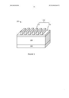
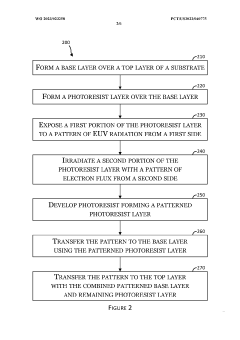
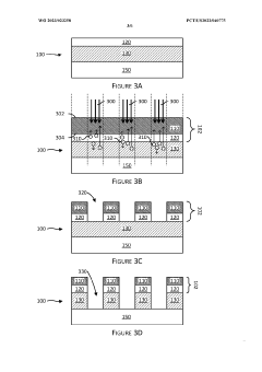
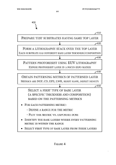
- The method involves forming a lithography stack with a silicon-based dielectric base layer and a photoresist layer, where the base layer acts as an electron booster to enhance exposure of the photoresist with energetic electrons, reducing the EUV radiation dose needed by 10-50% by promoting secondary exposure from below, thereby lowering the EUV radiation dose required for patterning.
Geopolitical Implications of EUV Technology
The geopolitical landscape surrounding EUV lithography has evolved into a critical dimension of international relations and economic security. As one of the most advanced semiconductor manufacturing technologies, EUV lithography has become a focal point in the technological competition between global powers. The United States, European Union, Japan, South Korea, and China are engaged in an increasingly complex struggle for technological supremacy, with EUV technology representing a strategic high ground.
The concentration of EUV expertise and manufacturing capabilities in specific regions has created significant geopolitical vulnerabilities. ASML, headquartered in the Netherlands, maintains a near-monopoly on EUV lithography systems, making it a strategic asset for the European Union while simultaneously becoming a target for technology transfer restrictions. The United States has leveraged its influence to prevent ASML from selling its most advanced EUV systems to China, demonstrating how this technology has become a tool in broader diplomatic and trade negotiations.
Export controls and technology sanctions related to EUV lithography have emerged as powerful instruments of foreign policy. These measures reflect growing concerns about national security implications of advanced semiconductor capabilities, particularly in military applications and critical infrastructure. The formation of technology alliances, such as the U.S.-led "Chip 4" alliance with Japan, South Korea, and Taiwan, illustrates how EUV technology access is reshaping international alignments and creating new geopolitical blocs centered around technological capabilities rather than traditional alliances.
The race to achieve self-sufficiency in semiconductor manufacturing has accelerated, with nations investing unprecedented sums in domestic chip production. The European Chips Act, America's CHIPS Act, and China's massive investments in its semiconductor industry all reflect the strategic imperative to control critical nodes in the semiconductor supply chain. This nationalization trend represents a significant shift away from the globalized production model that has characterized the industry for decades.
Regional tensions, particularly in East Asia, are increasingly influenced by the distribution of EUV capabilities. Taiwan's central position in advanced semiconductor manufacturing has elevated its geopolitical significance, with TSMC's EUV-based production capabilities becoming a factor in cross-strait relations and U.S.-China competition. The vulnerability of these concentrated manufacturing hubs to potential disruption—whether from natural disasters, pandemics, or military conflict—has highlighted the strategic risks inherent in the current geographic distribution of EUV technology.
Supply Chain Resilience for EUV Adoption
The resilience of the EUV lithography supply chain represents a critical factor in semiconductor industry dynamics, particularly as global adoption accelerates. ASML's position as the sole manufacturer of EUV lithography systems creates an inherent vulnerability in the ecosystem, with any disruption to their production capabilities potentially cascading throughout the semiconductor manufacturing landscape. This concentration risk is further amplified by the complex nature of EUV systems, which integrate thousands of precision components from specialized suppliers across multiple countries.
Recent global events have highlighted the fragility of technology supply chains, prompting semiconductor manufacturers to develop robust contingency plans for EUV implementation. These strategies typically include building inventory buffers of critical components, diversifying supplier relationships where possible, and establishing redundant manufacturing capabilities for key subsystems. Leading chip manufacturers have begun implementing dual-sourcing strategies for ancillary EUV components, though the core exposure systems remain single-sourced.
Geographic concentration presents another significant challenge, with key EUV components predominantly manufactured in Europe, North America, and East Asia. This distribution creates exposure to regional disruptions, whether from natural disasters, geopolitical tensions, or public health emergencies. The semiconductor industry has responded by advocating for government policies supporting domestic manufacturing capabilities and strategic stockpiling of critical components.
The complexity of EUV systems also introduces maintenance and service dependencies that affect supply chain resilience. The highly specialized nature of EUV maintenance requires dedicated technical expertise, creating potential bottlenecks in system uptime and productivity. Forward-thinking manufacturers have invested in comprehensive training programs and remote diagnostic capabilities to mitigate these risks.
Financial resilience represents another dimension of the EUV supply chain challenge. The substantial capital investment required for EUV adoption—with systems costing upwards of $150 million each—necessitates robust financial planning and risk management. Leading semiconductor manufacturers have developed phased implementation approaches that balance technological advancement with financial stability, often securing long-term purchase agreements to ensure system availability while managing capital expenditure timing.
As the industry continues its transition to EUV lithography, collaborative approaches to supply chain resilience have emerged. Industry consortia, public-private partnerships, and strategic alliances between manufacturers and suppliers are creating more robust ecosystems that can better withstand disruptions. These collaborative models represent a promising evolution in supply chain management for critical semiconductor manufacturing technologies.
Unlock deeper insights with PatSnap Eureka Quick Research — get a full tech report to explore trends and direct your research. Try now!
Generate Your Research Report Instantly with AI Agent
Supercharge your innovation with PatSnap Eureka AI Agent Platform!