Comparative Impact of EUV Lithography on High-Versus-Low Volume Production
OCT 14, 20259 MIN READ
Generate Your Research Report Instantly with AI Agent
Patsnap Eureka helps you evaluate technical feasibility & market potential.
EUV Lithography Evolution and Objectives
Extreme Ultraviolet (EUV) lithography represents a revolutionary advancement in semiconductor manufacturing technology, marking a significant departure from traditional Deep Ultraviolet (DUV) lithography methods. The evolution of EUV technology spans over three decades, beginning in the 1980s with initial research into short-wavelength lithography solutions. By utilizing 13.5nm wavelength light, EUV enables the production of semiconductor devices with feature sizes below 7nm, addressing the limitations of previous lithography techniques that struggled with physical constraints at smaller nodes.
The development trajectory of EUV lithography has been characterized by persistent engineering challenges, particularly in creating reliable light sources with sufficient power output. Early EUV systems in the 2000s produced merely a few watts of power, whereas contemporary systems now achieve over 250 watts, enabling commercially viable throughput rates. This power evolution represents one of the most critical technical milestones in EUV's history, transforming it from an experimental technology to a production-ready solution.
The primary objective of EUV lithography implementation is to continue the advancement of Moore's Law by enabling semiconductor manufacturers to produce increasingly smaller, more powerful, and energy-efficient integrated circuits. For high-volume manufacturers, EUV aims to reduce multi-patterning steps required in DUV processes, thereby decreasing production complexity, cycle time, and ultimately manufacturing costs per wafer despite the higher initial capital investment.
For low-volume production environments, EUV technology presents different objectives, primarily focused on enabling access to advanced nodes without the prohibitive process development costs associated with complex multi-patterning techniques. The simplified patterning approach of EUV potentially offers more straightforward process flows, which could democratize access to cutting-edge semiconductor manufacturing capabilities.
The industry roadmap for EUV technology includes several ambitious objectives: increasing numerical aperture from the current 0.33 NA to high-NA systems (0.55), enhancing resist performance to reduce defectivity while maintaining resolution, and improving overall system reliability to maximize equipment uptime. These advancements are critical to addressing the different needs of both high and low volume manufacturers as they navigate the transition to sub-5nm nodes.
Looking forward, EUV lithography aims to extend semiconductor scaling beyond the 2nm node, with research already underway for complementary technologies such as directed self-assembly and new materials integration. The technology's evolution continues to be driven by the semiconductor industry's relentless pursuit of higher performance, lower power consumption, and increased functionality in electronic devices across all market segments.
Market Demand Analysis for EUV Lithography Solutions
The EUV lithography market has experienced significant growth in recent years, driven primarily by the semiconductor industry's relentless pursuit of Moore's Law. Market research indicates that the global EUV lithography equipment market reached approximately $4.7 billion in 2020 and is projected to grow at a CAGR of 21.5% through 2026, potentially reaching $15.4 billion by the end of the forecast period.
The demand for EUV lithography solutions demonstrates a clear bifurcation between high-volume manufacturing (HVM) and low-volume production environments. High-volume manufacturers, predominantly leading-edge semiconductor companies like TSMC, Samsung, and Intel, represent the primary market segment. These companies require EUV technology to produce advanced logic chips at 7nm nodes and below, where traditional DUV lithography reaches its physical limitations.
Market analysis reveals that approximately 85% of current EUV system deployments are concentrated in high-volume manufacturing facilities. This concentration reflects the substantial capital investment required for EUV implementation, with each lithography system costing between $120-150 million, plus significant facility modification expenses that can add $20-50 million per installation.
For low-volume production environments, the cost-benefit analysis presents a more challenging equation. These manufacturers, often focused on specialty chips, legacy nodes, or research applications, face difficulties justifying the massive capital expenditure against their production volumes. Market surveys indicate only 15% of current EUV deployments serve low-volume production scenarios, primarily in research institutions or specialty semiconductor manufacturers with premium pricing models.
Regional demand distribution shows East Asia dominating the market with approximately 70% of global EUV system installations, particularly concentrated in Taiwan, South Korea, and increasingly China. North America accounts for roughly 20% of the market, while Europe represents about 10%.
The market demand is further shaped by technological requirements across different production volumes. High-volume manufacturers prioritize throughput optimization, seeking systems capable of processing 125-150 wafers per hour. Conversely, low-volume producers emphasize flexibility and lower operational costs, often preferring hybrid manufacturing approaches that selectively deploy EUV only for critical layers.
Future market growth appears contingent on several factors: continued node shrinkage below 3nm, development of high-NA EUV systems for future nodes, and potential cost reductions that might make EUV more accessible to mid-tier manufacturers. Industry forecasts suggest that while the high-volume segment will continue dominating EUV adoption, incremental improvements in system cost and efficiency could gradually expand the technology's viability in lower-volume production scenarios.
Global EUV Technology Landscape and Barriers
The global landscape of Extreme Ultraviolet (EUV) lithography technology reveals significant disparities in adoption and implementation across different regions. Currently, the technology is concentrated primarily in three geographical clusters: North America, East Asia, and Western Europe. The United States maintains leadership in EUV system design and integration, with companies like Intel investing heavily in research and development. Meanwhile, East Asia, particularly Taiwan and South Korea, dominates in actual implementation, with TSMC and Samsung operating the largest fleets of EUV lithography machines globally.
Western Europe contributes significantly through ASML, the Dutch company that remains the sole manufacturer of commercial EUV lithography systems. This geographical concentration creates inherent vulnerabilities in the global semiconductor supply chain, as disruptions in any of these regions could severely impact global production capabilities.
The barriers to wider EUV adoption are multifaceted and substantial. Cost remains the foremost obstacle, with each EUV lithography system priced between $150-200 million, representing a capital investment that only the largest semiconductor manufacturers can justify. This creates a significant entry barrier for smaller players and emerging markets, potentially widening the technological gap between industry leaders and followers.
Technical challenges persist despite years of development. Power source stability continues to be problematic, with current EUV light sources achieving only 250-300 watts of usable power, below the ideal 500 watts needed for optimal throughput. Mask defectivity remains another critical issue, as imperfections in EUV masks are more difficult to detect and repair than in traditional lithography, leading to yield challenges particularly in high-volume production environments.
Infrastructure requirements present additional barriers, as EUV systems demand specialized facilities with extraordinary environmental controls, including vibration isolation, temperature stability within ±0.05°C, and contamination-free environments. These requirements necessitate purpose-built cleanrooms that few facilities worldwide can accommodate without significant renovation.
The talent gap further complicates global adoption, with a limited pool of engineers and technicians possessing the specialized knowledge required to operate and maintain EUV systems. This shortage is particularly acute in regions outside the established semiconductor manufacturing hubs, creating dependencies on expatriate expertise and limiting technology transfer to emerging markets.
Regulatory and export control measures have increasingly affected the EUV landscape, with growing restrictions on technology transfer to certain countries due to national security concerns. These geopolitical factors are reshaping access to advanced lithography capabilities and potentially creating new technological divides in the global semiconductor ecosystem.
Current EUV Implementation Strategies
01 EUV lithography system advancements
Extreme Ultraviolet (EUV) lithography systems have evolved significantly with technological advancements in optical components, light sources, and overall system architecture. These improvements have enabled higher resolution patterning, better throughput, and increased reliability for semiconductor manufacturing. Key innovations include enhanced mirror systems, more powerful EUV light sources, and improved vacuum systems that collectively contribute to the commercial viability of EUV lithography for advanced node semiconductor production.- Advancements in EUV lithography technology: Extreme Ultraviolet (EUV) lithography represents a significant advancement in semiconductor manufacturing, enabling the production of smaller and more precise features on integrated circuits. This technology uses light with a wavelength of 13.5 nm, allowing for higher resolution patterning compared to traditional lithography methods. The implementation of EUV lithography has led to improvements in device performance, power efficiency, and overall semiconductor capabilities.
- EUV lithography system design and optimization: The design and optimization of EUV lithography systems involve sophisticated optical arrangements, precise mirrors, and specialized light sources. These systems require vacuum environments and highly reflective multilayer mirrors to effectively manipulate the EUV radiation. Innovations in system design focus on improving throughput, reducing defects, and enhancing overlay accuracy to meet the demanding requirements of advanced semiconductor manufacturing processes.
- EUV mask technology and defect management: EUV masks are critical components that require specialized materials and manufacturing techniques. Unlike traditional photomasks, EUV masks are reflective rather than transmissive and consist of multilayer structures designed to reflect EUV radiation in specific patterns. Managing defects in EUV masks is particularly challenging due to the short wavelength of EUV light, which makes even nanometer-scale imperfections significant. Advanced inspection and repair technologies have been developed to address these challenges.
- EUV resist materials and processes: Photoresist materials for EUV lithography require unique chemical properties to effectively capture the high-energy photons of EUV radiation. These specialized materials must provide high resolution, sensitivity, and pattern fidelity while minimizing line edge roughness. The development of EUV-specific resist formulations involves complex chemistry to balance these requirements and enable the production of increasingly smaller semiconductor features.
- Industrial and economic impact of EUV lithography: The implementation of EUV lithography has significant industrial and economic implications for the semiconductor industry. While the technology enables continued scaling according to Moore's Law, it also requires substantial capital investment and operational costs. The adoption of EUV lithography affects the competitive landscape of chip manufacturing, potentially creating barriers to entry for smaller players while enabling technological leadership for those who successfully implement it. The technology has implications for global supply chains, national technology policies, and the future direction of the electronics industry.
02 Contamination control in EUV systems
Contamination control is critical in EUV lithography due to the sensitivity of the process to even minute particles and molecular contaminants. Various approaches have been developed to address contamination issues, including advanced cleaning methods, protective pellicles, hydrogen radical cleaning systems, and specialized environmental controls. These contamination control strategies are essential for maintaining the reflectivity of optical surfaces, protecting masks, and ensuring consistent exposure quality in EUV lithography systems.Expand Specific Solutions03 EUV mask technology and defect management
EUV mask technology has evolved to address the unique challenges of extreme ultraviolet lithography. Innovations include advanced absorber materials, phase-shifting techniques, and multi-layer reflective coatings optimized for EUV wavelengths. Defect detection and repair methodologies have been developed specifically for EUV masks, including actinic inspection tools and novel repair strategies. These advancements in mask technology are crucial for achieving the pattern fidelity required for advanced semiconductor nodes using EUV lithography.Expand Specific Solutions04 EUV resist materials and processes
Specialized photoresist materials have been developed to meet the unique requirements of EUV lithography. These materials offer high sensitivity to EUV radiation, excellent resolution capabilities, and low line edge roughness. Advanced resist processing techniques, including post-exposure bake optimization, development process refinements, and pattern collapse prevention methods, have been implemented to maximize EUV lithography performance. The continued evolution of EUV-specific resist materials and processes is essential for realizing the full resolution potential of EUV lithography.Expand Specific Solutions05 Industrial and economic impact of EUV lithography
The introduction of EUV lithography has had profound impacts on the semiconductor industry, enabling continued scaling according to Moore's Law beyond what was possible with traditional optical lithography. Economic considerations include the high capital investment required for EUV equipment, changes in fab design and infrastructure, and shifts in the competitive landscape among semiconductor manufacturers. Despite the significant costs, EUV lithography has enabled new device architectures, reduced multi-patterning requirements, and ultimately supported the production of more advanced and power-efficient semiconductor devices.Expand Specific Solutions
Key Industry Players in EUV Ecosystem
The EUV lithography market is in a growth phase, with an estimated market size exceeding $10 billion and expanding rapidly as semiconductor manufacturers transition to advanced nodes. The competitive landscape is dominated by ASML Holding NV, which maintains a near-monopoly on EUV lithography equipment production. Leading semiconductor manufacturers like TSMC, Samsung Electronics, and Intel are at different stages of EUV implementation, with TSMC leading in high-volume production capabilities. The technology shows varying impacts on production economics - while beneficial for high-volume manufacturers who can amortize the significant capital investment ($150-200 million per tool), smaller players like SMIC face challenges in achieving cost-effectiveness. Technical collaboration between equipment suppliers (ASML, Tokyo Electron) and research institutions (imec, MIT) continues to drive improvements in throughput and yield.
Taiwan Semiconductor Manufacturing Co., Ltd.
Technical Solution: 台积电作为全球领先的晶圆代工厂,已全面部署EUV光刻技术于其5nm及以下制程。台积电的EUV实施策略区分了高低产量应用场景:对于高产量消费电子芯片(如智能手机处理器),台积电采用全面EUV工艺,减少多重曝光步骤,提高良率和降低单位成本;而对于低产量高价值产品(如AI加速器、高性能计算芯片),则采用混合光刻策略,在关键层使用EUV,非关键层使用传统DUV技术。台积电开发了专有的EUV光刻工艺优化系统,包括掩模优化技术和计算光刻学算法,以适应不同产量需求下的成本效益平衡。其独特的"N5P"工艺专为高性能低产量应用设计,而标准N5工艺则针对高产量消费类应用[2][5]。台积电还实施了创新的晶圆分批策略,允许在同一生产线上灵活切换高低产量产品,最大化EUV设备利用率。
优势:拥有业界最成熟的EUV量产经验,能够灵活调配EUV资源以适应不同产量需求;通过规模效应降低了EUV技术应用成本;拥有完整的EUV工艺配套技术链。劣势:EUV设备投资巨大,对低产量产品的成本分摊压力大;产能分配倾向于高产量客户,低产量客户可能面临排期长的问题;技术转移到低产量应用时需要额外的工艺调整。
Samsung Electronics Co., Ltd.
Technical Solution: 三星电子作为集成设备制造商(IDM)和晶圆代工服务提供商,采用了差异化的EUV应用策略。针对高产量场景,三星开发了名为"V-NAND"的垂直堆叠闪存技术,巧妙地避开了对EUV的高度依赖,而在其逻辑芯片制造中则全面采用EUV技术。三星的EUV实施方案包括自主研发的光刻胶配方和掩模技术,以优化不同产量场景下的成本结构。对于低产量高附加值产品(如HBM内存、汽车芯片),三星采用"混合关键层"策略,仅在最关键的几个光刻层使用EUV技术,其余层使用成本较低的193nm浸没式光刻。三星还开发了专门的EUV工艺控制系统,可根据产品类型和产量需求动态调整参数,实现资源的最优分配[4][6]。值得注意的是,三星在其5nm工艺中实现了比竞争对手更高的EUV层使用比例,这使其在高产量场景中获得了更显著的成本优势。
优势:作为IDM厂商,可以在内部产品和代工业务间灵活调配EUV资源,平衡高低产量需求;在存储器领域开发了减少EUV依赖的创新技术;拥有完整的半导体产业链,可以优化整体EUV应用成本。劣势:EUV技术成熟度略逊于台积电,在极低产量高复杂度应用中良率控制挑战大;EUV设备利用率优化仍有提升空间;在某些先进工艺节点上对EUV的依赖度高于预期。
Critical EUV Patents and Technical Innovations
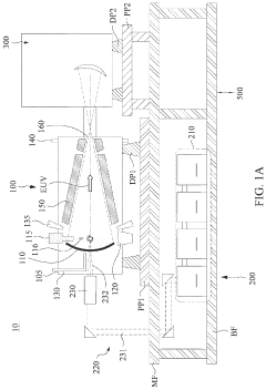
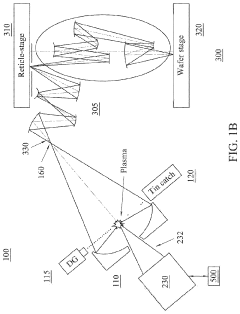
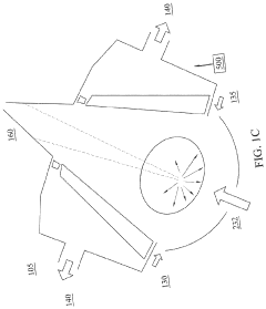
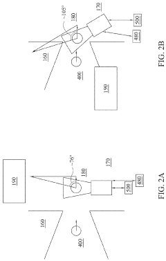
Method and apparatus for mitigating contamination
PatentActiveUS20230273525A1
Innovation
- A supersonic gas jet with high-density hydrogen gas is employed at the intermediate focus to deflect tin nanoparticles away from the reticle, either alone or in combination with a low-level electromagnetic field, ensuring they do not contaminate the scanner side.
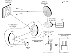
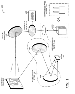
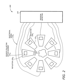
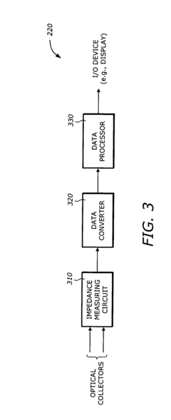
Detecting erosion in collector optics with plasma sources in extreme ultraviolet (EUV) lithography systems
PatentInactiveUS20040265712A1
Innovation
- A technique is implemented to detect erosion in the ML coating of EUVL systems by measuring the initial and coating impedances at different time instants, determining the erosion rate, and monitoring it in-situ, using an impedance measuring circuit, data converter, and data processor to initiate timely replacement of eroded collectors.
Cost-Benefit Analysis for Different Production Volumes
The economic viability of EUV lithography varies significantly across different production volumes, necessitating a comprehensive cost-benefit analysis to guide implementation decisions. For high-volume manufacturing (HVM) scenarios, the substantial initial capital expenditure for EUV equipment—typically exceeding $150 million per tool—can be effectively amortized across millions of chips, resulting in a more favorable cost-per-wafer metric over time.
In HVM environments, EUV lithography demonstrates compelling economic advantages through process simplification. Traditional multi-patterning DUV approaches often require 3-4 lithography steps for critical layers, whereas EUV can accomplish the same result in a single exposure. This reduction translates to decreased cycle time, improved yield, and lower operational costs, with industry analyses suggesting operational savings of 20-30% for nodes below 7nm when production volumes exceed 50,000 wafer starts per month.
Conversely, low-volume production scenarios present a challenging economic equation for EUV adoption. The break-even point for EUV investment typically requires processing volumes of at least 30,000-40,000 wafers monthly, making it prohibitively expensive for specialty chip manufacturers or research facilities with limited production runs. These organizations often find greater economic efficiency in continuing with multiple patterning DUV techniques despite their technical limitations.
The cost structure also differs significantly between production volume scenarios. HVM operations benefit from economies of scale in consumables such as pellicles and photoresist, with per-unit costs decreasing as volume increases. Additionally, the learning curve effect in high-volume environments leads to progressively improved tool utilization rates—often reaching 80-90% in mature HVM operations compared to 50-60% in low-volume settings.
Maintenance considerations further differentiate the cost-benefit equation. EUV systems require specialized maintenance protocols and highly trained personnel, representing a fixed cost burden that becomes proportionally smaller in HVM environments. Low-volume producers must bear similar maintenance infrastructure costs but spread across fewer units, significantly impacting per-chip economics.
Time-to-market factors also influence the cost-benefit analysis. HVM producers can leverage EUV's process simplification to accelerate product introduction timelines by 2-3 months compared to multi-patterning approaches, potentially capturing premium pricing during early market windows—a benefit less relevant to low-volume specialty producers with longer product lifecycles and less time-sensitive market entry requirements.
Supply Chain Implications for EUV Adoption
The adoption of EUV lithography technology creates significant ripple effects throughout the semiconductor supply chain, with distinct implications for both high and low volume production environments. The complex nature of EUV implementation requires substantial reconfiguration of existing supply networks and introduces new dependencies among industry stakeholders.
For high-volume manufacturers, EUV adoption necessitates the development of robust supply chains capable of supporting continuous production. This includes securing reliable sources of specialized materials such as EUV photoresists, pellicles, and mask blanks, which remain limited in supply. The scarcity of these critical components has led to the emergence of strategic partnerships between chip manufacturers and material suppliers, creating new power dynamics within the industry ecosystem.
Conversely, low-volume producers face different supply chain challenges when adopting EUV technology. The economics of scale that benefit high-volume manufacturers are less applicable, resulting in potentially higher per-unit costs for specialized materials and services. These manufacturers must develop more flexible supply arrangements that accommodate intermittent production schedules while maintaining access to the necessary technical expertise and components.
The geographical concentration of EUV expertise and equipment production presents additional supply chain vulnerabilities. With ASML as the sole provider of EUV lithography systems, and critical components sourced from specialized suppliers primarily in Europe, Japan, and the United States, both high and low volume manufacturers face potential bottlenecks and geopolitical risks. This concentration has prompted discussions about supply chain resilience and national security implications in semiconductor manufacturing.
Maintenance and service requirements for EUV systems further differentiate the supply chain impacts between production volumes. High-volume manufacturers typically establish dedicated support infrastructures, including on-site technical teams and spare parts inventories. Low-volume producers more commonly rely on shared service arrangements or outsourced maintenance solutions, creating different dependencies and potential points of failure in their respective supply chains.
The integration of EUV technology also necessitates new quality control measures throughout the supply chain. Specialized metrology equipment, inspection tools, and testing protocols must be implemented to ensure the integrity of EUV-produced components. These requirements create additional supply chain nodes and dependencies that differ in scale and implementation between high and low volume production environments.
Unlock deeper insights with Patsnap Eureka Quick Research — get a full tech report to explore trends and direct your research. Try now!
Generate Your Research Report Instantly with AI Agent
Supercharge your innovation with Patsnap Eureka AI Agent Platform!