The Strategic Importance of EUV Lithography in Tech Patents
OCT 14, 20259 MIN READ
Generate Your Research Report Instantly with AI Agent
Patsnap Eureka helps you evaluate technical feasibility & market potential.
EUV Lithography Evolution and Strategic Objectives
Extreme Ultraviolet (EUV) lithography represents a revolutionary advancement in semiconductor manufacturing technology, marking a significant departure from traditional Deep Ultraviolet (DUV) lithography methods. The evolution of this technology can be traced back to the early 1990s when researchers began exploring alternative lithography techniques to overcome the physical limitations of conventional optical lithography. The journey from concept to commercial implementation has spanned nearly three decades, characterized by persistent technical challenges and collaborative industry efforts.
The development trajectory of EUV lithography has been closely aligned with Moore's Law, which predicts the doubling of transistor density approximately every two years. As semiconductor manufacturers pushed toward smaller node sizes below 10nm, the limitations of traditional immersion lithography became increasingly apparent, necessitating the shift toward EUV technology capable of achieving feature sizes of 7nm and below with greater precision.
A critical milestone in EUV evolution occurred in 2016-2017 when ASML delivered the first production-ready EUV lithography systems, enabling the transition from research to commercial application. This breakthrough came after years of addressing fundamental challenges related to light source power, mask infrastructure, and resist performance. The subsequent years have witnessed rapid adoption across leading semiconductor manufacturers, with EUV becoming essential for advanced node production.
The strategic objectives driving EUV lithography development extend beyond mere technical advancement. Primary among these is maintaining the semiconductor industry's ability to deliver continued performance improvements while managing manufacturing costs. EUV technology enables the production of more complex chip designs with fewer process steps compared to multi-patterning approaches required with DUV lithography, potentially offering economic advantages despite higher initial equipment investments.
Another key objective is securing technological leadership in the highly competitive semiconductor industry. Nations and corporations that master EUV lithography gain significant advantages in producing cutting-edge chips for applications in artificial intelligence, high-performance computing, and advanced mobile devices. This technological capability has increasingly become intertwined with national security interests and economic competitiveness on the global stage.
Looking forward, the industry aims to extend EUV capabilities through high-NA (numerical aperture) EUV systems, which promise to enable feature sizes below 3nm. This next evolution represents a critical pathway for continuing Moore's Law scaling beyond current limitations, with significant research and development investments already underway to realize these systems by mid-decade.
Semiconductor Industry Demand for Advanced Lithography
The semiconductor industry's demand for advanced lithography technologies has been growing exponentially as manufacturers strive to maintain the trajectory predicted by Moore's Law. EUV (Extreme Ultraviolet) lithography represents a critical inflection point in this pursuit, enabling the production of increasingly miniaturized and complex semiconductor components. Market analysis indicates that the global semiconductor industry, valued at approximately $573 billion in 2022, is projected to reach $1.38 trillion by 2029, with advanced lithography systems serving as a key enabler of this growth.
The primary market driver for EUV lithography stems from the insatiable demand for higher computing power in smaller form factors across multiple sectors. Consumer electronics manufacturers require chips with greater transistor density to power next-generation smartphones, tablets, and wearable devices. The automotive industry increasingly depends on advanced semiconductors for autonomous driving capabilities, infotainment systems, and electrification technologies.
Data centers and cloud computing infrastructure represent another significant market segment, with the exponential growth in data processing requirements necessitating more powerful and energy-efficient semiconductor solutions. The artificial intelligence and machine learning revolution has further accelerated demand for specialized chips capable of handling complex computational tasks, which can only be manufactured using cutting-edge lithography techniques.
Geographically, East Asia dominates the demand landscape, with Taiwan, South Korea, and increasingly China investing heavily in semiconductor manufacturing capabilities. TSMC and Samsung have emerged as the primary adopters of EUV lithography technology, driving significant portions of the market demand. North America maintains strong demand through companies like Intel, while Europe's semiconductor strategy aims to reduce dependency on foreign suppliers by developing domestic advanced manufacturing capabilities.
Industry forecasts suggest that the EUV lithography equipment market specifically will grow at a CAGR of approximately 21.5% through 2028. This growth trajectory reflects the industry's recognition that EUV represents the only viable path forward for continuing miniaturization beyond the 7nm node. The high capital expenditure associated with EUV implementation—with each lithography system costing upwards of $150 million—has created significant barriers to entry, concentrating demand among a small number of leading-edge manufacturers.
The COVID-19 pandemic and subsequent global chip shortage have further highlighted the strategic importance of advanced semiconductor manufacturing capabilities, prompting governments worldwide to incentivize domestic production through substantial subsidies and investment programs. This governmental support has accelerated demand for advanced lithography solutions as countries compete for technological sovereignty in the semiconductor space.
Global EUV Technology Landscape and Barriers
Extreme Ultraviolet (EUV) lithography represents a revolutionary advancement in semiconductor manufacturing, with its global technology landscape characterized by significant geographic concentration. Currently, the Netherlands-based ASML holds a virtual monopoly on EUV lithography systems, creating a critical bottleneck in the global semiconductor supply chain. This concentration of expertise presents substantial geopolitical implications, particularly amid increasing technological competition between the United States and China.
In Asia, Japan has established itself as a key player in the EUV ecosystem through companies like Canon and Nikon, which focus on complementary technologies and components. South Korea, home to Samsung and SK Hynix, has made substantial investments in EUV implementation but remains dependent on foreign technology. Taiwan, through TSMC, has become the world's most advanced adopter of EUV lithography for commercial chip production.
The United States maintains leadership in EUV light source technology and critical components through companies like Intel and Cymer (now part of ASML). Meanwhile, China faces significant barriers to EUV access due to export restrictions, forcing alternative technology development paths that may ultimately diverge from global standards.
Technical barriers to wider EUV adoption remain substantial. Power source limitations continue to challenge the industry, as current EUV systems operate at approximately 250 watts, while optimal efficiency would require 500+ watts. Mask defectivity presents another significant hurdle, as imperfections at the nanometer scale can render entire chip designs unusable, necessitating complex inspection and repair technologies.
Photoresist performance limitations further complicate EUV implementation, with current materials struggling to achieve the perfect balance between sensitivity, resolution, and line edge roughness. The extreme precision required for EUV mirrors and optics (with surface irregularities limited to less than 50 picometers) represents perhaps the most formidable manufacturing challenge in modern technology.
Economic barriers are equally significant, with each EUV lithography system costing approximately $150-200 million, plus substantial facility modification expenses. This creates a prohibitive entry barrier for all but the largest semiconductor manufacturers. Additionally, the complex supply chain for EUV systems involves over 5,000 parts from more than 700 suppliers across 20 countries, making the technology vulnerable to trade disruptions and geopolitical tensions.
Knowledge barriers further restrict EUV proliferation, as the technology requires highly specialized expertise in quantum physics, materials science, and precision engineering. The limited pool of qualified engineers and scientists capable of working with EUV systems ensures that technology transfer remains challenging even when not restricted by export controls.
Current EUV Implementation Approaches
01 EUV Lithography System Components
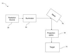
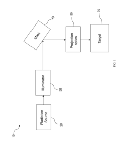
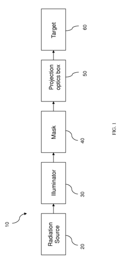
Extreme Ultraviolet (EUV) lithography systems comprise specialized components designed to work with short-wavelength light. These systems include EUV light sources, reflective optical elements, specialized masks, and precision positioning stages. The components are engineered to maintain extreme accuracy in nanometer-scale semiconductor manufacturing while operating in vacuum environments necessary for EUV wavelengths.- EUV Lithography System Design and Components: EUV lithography systems incorporate specialized components designed to work with extreme ultraviolet light. These systems typically include radiation sources, illumination optics, projection optics, and wafer stages. The design focuses on maintaining precise alignment and stability while managing the challenges of working with EUV wavelengths. Advanced control systems ensure accurate positioning and exposure during the lithography process.
- EUV Radiation Source Technology: EUV lithography requires specialized radiation sources capable of generating extreme ultraviolet light at specific wavelengths (typically 13.5nm). These sources often utilize laser-produced plasma or discharge-produced plasma technologies. The development focuses on increasing source power while maintaining stability, reducing debris generation, and extending operational lifetime to meet the demands of high-volume manufacturing environments.
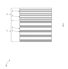
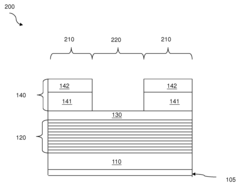
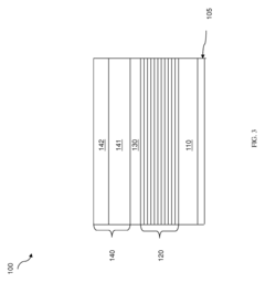
- EUV Mask and Reticle Technology: EUV masks and reticles are critical components that contain the circuit patterns to be transferred onto silicon wafers. Unlike traditional optical lithography masks, EUV masks are reflective rather than transmissive and require specialized multilayer coatings to efficiently reflect EUV radiation. Technologies focus on defect inspection, repair methods, and protection systems to maintain mask integrity throughout the manufacturing process.
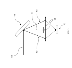
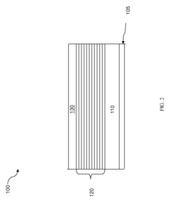
- EUV Optical Systems and Mirror Technology: EUV lithography employs sophisticated optical systems with specialized mirrors rather than traditional lenses. These mirrors feature multilayer coatings designed to reflect EUV wavelengths with maximum efficiency. The optical systems must maintain extreme precision while compensating for thermal effects and mechanical vibrations. Advanced technologies focus on improving mirror reflectivity, reducing wavefront errors, and enhancing overall system stability.
- EUV Resist and Process Integration: EUV lithography requires specialized photoresist materials optimized for extreme ultraviolet wavelengths. These resists must deliver high resolution, sensitivity, and pattern fidelity while minimizing line edge roughness. Process integration technologies address challenges such as stochastic effects, outgassing control, and compatibility with existing semiconductor manufacturing workflows to enable high-volume production with acceptable yields.
02 EUV Source Technology
EUV light sources typically utilize laser-produced plasma or discharge-produced plasma to generate the extreme ultraviolet radiation needed for lithography. These sources involve striking tin, xenon or other target materials with high-energy lasers or electrical discharges to create plasma that emits EUV radiation. The technology includes sophisticated debris mitigation systems and collector optics to efficiently capture and direct the EUV light to the lithography system.Expand Specific Solutions03 EUV Mask and Reticle Technology
EUV masks differ significantly from traditional optical lithography masks, employing reflective rather than transmissive designs. These masks consist of multilayer reflective coatings on ultra-flat substrates with absorber patterns that define circuit features. Advanced technologies address challenges such as defect inspection, repair methods, and pattern fidelity at extreme scales. Innovations include phase-shifting techniques and novel absorber materials to enhance contrast and resolution.Expand Specific Solutions04 EUV Optical Systems and Alignment
EUV optical systems employ complex arrangements of multilayer mirrors rather than traditional lenses, as EUV light is absorbed by most materials. These systems require unprecedented precision in alignment and positioning, with tolerances in the sub-nanometer range. Advanced metrology systems continuously monitor and adjust the optical path to compensate for thermal effects, mechanical vibrations, and other disturbances that could affect imaging quality.Expand Specific Solutions05 EUV Resist and Process Integration
Specialized photoresist materials have been developed to work with the unique properties of EUV radiation. These resists must achieve high sensitivity while maintaining resolution and line-edge roughness requirements. Process integration challenges include optimizing exposure dose, developing post-exposure bake procedures, and managing pattern collapse at extremely small dimensions. Advanced computational modeling helps predict and optimize resist performance under EUV exposure conditions.Expand Specific Solutions
Leading Companies in EUV Lithography Ecosystem
EUV lithography represents a critical technological frontier in semiconductor manufacturing, currently in its early maturity phase with rapid adoption accelerating. The market is experiencing robust growth, projected to reach $10-15 billion by 2025, driven by increasing demand for advanced chips with smaller nodes. The competitive landscape is dominated by ASML Netherlands BV, which holds a near-monopoly on EUV lithography equipment manufacturing, while semiconductor giants like TSMC, Samsung Electronics, and Intel are the primary implementers. Other players including Applied Materials, Tokyo Electron, and SMIC are developing complementary technologies. Asian manufacturers, particularly TSMC and Samsung, lead in commercial deployment, while Western companies focus on innovation and equipment development. The technology remains highly specialized with significant barriers to entry, creating a concentrated competitive environment where strategic partnerships and intellectual property portfolios determine market positioning.
Taiwan Semiconductor Manufacturing Co., Ltd.
Technical Solution: TSMC has developed proprietary EUV implementation methodologies that optimize the technology for mass production of advanced semiconductor nodes. Their approach includes specialized multi-patterning techniques that combine EUV with complementary patterning strategies to achieve sub-5nm features. TSMC's patented innovations include EUV-specific photoresist formulations that enhance sensitivity while maintaining resolution, custom pellicle solutions that protect masks from contamination while minimizing transmission loss, and advanced computational lithography algorithms that correct for process variations. Their N5 and N3 process nodes heavily leverage EUV technology, with the N3 node utilizing up to 30+ EUV layers. TSMC has also pioneered EUV-specific design-technology co-optimization methodologies that enable chip designers to maximize the benefits of EUV while minimizing its limitations.
Strengths: Industry-leading implementation expertise with proven high-volume manufacturing capability; extensive patent portfolio covering practical EUV applications; strong financial position enabling continued investment. Weaknesses: Dependency on ASML for equipment; geopolitical vulnerabilities due to concentration of advanced manufacturing in Taiwan; high capital expenditure requirements for maintaining technology leadership.
Samsung Electronics Co., Ltd.
Technical Solution: Samsung has developed a comprehensive EUV implementation strategy focused on memory and logic applications. Their approach includes specialized EUV process integration techniques for high-aspect-ratio features critical for DRAM manufacturing. Samsung's patented innovations include customized EUV mask architectures that enhance pattern fidelity for memory-specific layouts, novel materials systems that optimize EUV absorption and reduce line edge roughness, and integrated metrology solutions for real-time process control. Their V-NAND technology utilizes EUV for critical dimensions in peripheral circuitry, while their foundry business employs EUV extensively in their 5nm and 3nm process nodes. Samsung has also developed proprietary computational lithography techniques that compensate for EUV-specific stochastic effects, enabling higher yields in mass production environments.
Strengths: Vertical integration allowing coordinated development across materials, equipment and devices; diversified application across memory and logic products; strong patent position. Weaknesses: Slightly trailing TSMC in advanced logic process implementation; high capital intensity requiring continuous investment; challenges in achieving consistent yields at leading-edge nodes.
Critical Patents and Technical Innovations in EUV
Extreme Ultraviolet Lithography Process and Mask
PatentActiveUS20150168845A1
Innovation
- The implementation of a nearly on-axis illumination with partial coherence less than 0.3 in an EUV lithography system, combined with an EUV mask featuring a first region with main polygons and a second region with sub-resolution polygons, and a spatial filter to remove most non-diffracted light, enhancing spatial frequency resolution and uniformity of exposure intensity.
Extreme ultraviolet lithography process and mask
PatentActiveUS9448491B2
Innovation
- A mask structure incorporating a reflective multilayer with a flare-suppressing absorption stack (FSAS) and a flare-suppressing-by-phase-shifting (FSbPhS) layer, which absorbs EUV light and induces destructive interference to suppress OOB radiation, specifically DUV flare, enhancing image contrast and lithography performance.
Patent Strategy and Intellectual Property Considerations
EUV lithography represents a critical inflection point in semiconductor intellectual property strategy. Companies investing in EUV patents are establishing formidable barriers to entry while securing their position in advanced manufacturing capabilities. The patent landscape surrounding EUV technology has become increasingly complex, with key players like ASML, Samsung, TSMC, and Intel aggressively filing patents across the entire EUV ecosystem - from light sources to photoresist chemistry.
Strategic patent portfolio development in EUV technology requires a multi-layered approach. Organizations must balance between fundamental process patents and application-specific innovations. The most valuable portfolios combine core technology patents with complementary innovations in adjacent areas such as computational lithography, metrology, and materials science, creating comprehensive protection networks.
Cross-licensing agreements have emerged as essential business strategies in the EUV space, reflecting the distributed nature of innovation across the semiconductor ecosystem. No single entity controls all necessary intellectual property, necessitating collaborative arrangements that balance IP monetization with technology access. These agreements often include field-of-use restrictions that preserve competitive advantages in specific market segments.
Patent thickets surrounding EUV technology present significant freedom-to-operate challenges. Companies must conduct thorough landscape analyses before committing to EUV implementation pathways. Defensive patenting strategies have become increasingly important, with companies filing patents not necessarily for direct monetization but to secure negotiating leverage in potential disputes.
Geographic considerations play a crucial role in EUV patent strategy. While the United States, Japan, and Europe have traditionally dominated semiconductor IP, China's growing investments in domestic semiconductor capabilities have shifted the global patent landscape. Strategic filing decisions must account for manufacturing locations, market access priorities, and enforcement realities.
Time-to-market considerations heavily influence EUV patent strategies. The rapid pace of semiconductor advancement means companies must balance thorough patent protection with speed of innovation. Many organizations employ provisional patent applications and continuation strategies to maintain flexibility while establishing priority dates for their innovations.
Trade secret protection complements patent strategies for EUV implementation, particularly for manufacturing process details that are difficult to reverse-engineer from end products. Companies must carefully evaluate which aspects of their EUV technology stack are better protected through patents versus trade secrets, creating integrated IP protection frameworks.
Geopolitical Implications of EUV Technology Control
The control of Extreme Ultraviolet (EUV) lithography technology has emerged as a critical geopolitical lever in the global semiconductor industry. As nations recognize the strategic importance of advanced chip manufacturing capabilities, EUV technology has become a focal point of international technology competition and diplomacy. The Netherlands-based ASML's near-monopoly on EUV lithography machines has transformed what might otherwise be purely commercial technology into a geopolitical asset of immense value.
The United States has actively worked to restrict China's access to EUV technology through export controls and diplomatic pressure on allies, particularly the Netherlands and Japan. These restrictions aim to maintain Western technological superiority and prevent advanced semiconductor manufacturing capabilities from enhancing China's military and surveillance systems. This technology containment strategy represents a significant shift from previous decades of relatively open technology transfer in the semiconductor industry.
China's response has been multifaceted, combining aggressive investment in domestic alternatives, diplomatic protests, and attempts to acquire technology through various channels. The country has committed billions to developing indigenous lithography capabilities through initiatives like the "Made in China 2025" plan, though significant technical gaps remain. This technological decoupling is accelerating the fragmentation of global supply chains into distinct spheres of influence.
For multinational corporations, navigating this complex landscape requires sophisticated compliance systems and strategic planning. Companies must balance access to China's massive market against increasingly stringent export control regimes from Western governments. Patent strategies are being recalibrated to protect intellectual property while maintaining global competitiveness in a fragmenting technological ecosystem.
The EUV control regime also highlights the vulnerability of global supply chains to geopolitical tensions. Even companies outside direct EUV manufacturing face potential disruptions as restrictions cascade through interdependent technology ecosystems. This has prompted calls for supply chain resilience and redundancy across the semiconductor industry.
Looking forward, the geopolitical implications of EUV technology control will likely intensify as semiconductors become even more central to economic and military power. Nations without access to cutting-edge lithography may face significant constraints on their technological development and economic competitiveness. This technology-based stratification could reshape global power dynamics and alliance structures in the coming decades, making EUV lithography not merely an industrial asset but a defining element of 21st-century geopolitical competition.
Unlock deeper insights with Patsnap Eureka Quick Research — get a full tech report to explore trends and direct your research. Try now!
Generate Your Research Report Instantly with AI Agent
Supercharge your innovation with Patsnap Eureka AI Agent Platform!