The Seismic Shift in Patent Activity Due to EUV Lithography Breakthroughs
OCT 14, 20259 MIN READ
Generate Your Research Report Instantly with AI Agent
Patsnap Eureka helps you evaluate technical feasibility & market potential.
EUV Lithography Evolution and Objectives
Extreme Ultraviolet (EUV) lithography represents one of the most significant technological breakthroughs in semiconductor manufacturing over the past decade. The evolution of this technology can be traced back to the early 1990s when researchers began exploring alternatives to traditional optical lithography as feature sizes approached fundamental physical limits. The journey from concept to commercial implementation spans nearly three decades, marked by persistent technical challenges and collaborative industry efforts.
The initial development phase (1990-2005) focused primarily on fundamental research into EUV light sources, optics, and resist materials. During this period, the technology remained largely theoretical with significant hurdles in generating sufficient power and creating practical manufacturing tools. The intermediate development phase (2006-2016) saw increased investment from major semiconductor companies and equipment manufacturers, resulting in the first prototype systems capable of demonstrating basic EUV patterning capabilities.
The breakthrough period began around 2017 when ASML delivered the first commercial EUV lithography systems with sufficient reliability and throughput for limited production use. This milestone triggered an acceleration in patent activity across the semiconductor ecosystem, with filings increasing by approximately 300% between 2017 and 2022 compared to the previous five-year period.
The primary technical objective of EUV lithography has been to enable continued semiconductor scaling according to Moore's Law by providing a manufacturing method capable of producing features below 10nm. Specific goals include achieving resolution below 13.5nm wavelength, developing high-sensitivity photoresists compatible with EUV exposure, and creating mask infrastructure with near-zero defects.
Current technical objectives focus on improving system throughput (targeting >125 wafers per hour), reducing operational costs, and extending EUV technology to enable multiple patterning techniques for sub-3nm node manufacturing. The industry is also pursuing high-numerical-aperture EUV (High-NA EUV) systems to further extend resolution capabilities for future technology nodes.
The evolution trajectory suggests that EUV technology will remain central to advanced semiconductor manufacturing for at least the next decade, with continuous improvements in resolution, throughput, and cost-effectiveness. Patent activity indicates growing interest in complementary technologies that enhance EUV capabilities, including computational lithography, novel resist chemistries, and advanced metrology solutions specifically designed for EUV processes.
Market Demand Analysis for Advanced Semiconductor Manufacturing
The semiconductor industry's demand for advanced manufacturing technologies has been experiencing unprecedented growth, driven primarily by the continuous miniaturization of integrated circuits and the increasing complexity of electronic devices. EUV (Extreme Ultraviolet) lithography represents a revolutionary breakthrough in this domain, enabling the production of chips with feature sizes below 7nm. This technological advancement has created a substantial market pull across multiple sectors.
The global semiconductor manufacturing equipment market, valued at approximately $103 billion in 2022, is projected to reach $150 billion by 2027, with EUV lithography systems accounting for a significant portion of this growth. Major semiconductor manufacturers including TSMC, Samsung, and Intel have collectively invested over $20 billion in EUV technology implementation, highlighting the critical market demand for this advanced manufacturing capability.
Consumer electronics continues to be the primary driver of demand for EUV-enabled semiconductor manufacturing. The smartphone market alone requires over 1.4 billion advanced chips annually, with each new generation demanding higher performance and lower power consumption that only EUV lithography can deliver. Additionally, the high-performance computing sector has emerged as a rapidly growing market segment, with annual growth rates exceeding 20% due to artificial intelligence and data center expansions.
The automotive industry represents another significant market driver, as modern vehicles increasingly incorporate advanced driver assistance systems and autonomous driving capabilities. Each premium vehicle now contains up to 100 semiconductor chips, with this number expected to double by 2030, creating substantial demand for EUV-manufactured components.
Geographic distribution of market demand shows Asia-Pacific leading with 65% of global advanced semiconductor manufacturing capacity, followed by North America at 18% and Europe at 10%. China's ambitious semiconductor self-sufficiency initiatives have further intensified market competition and demand for advanced manufacturing technologies.
Supply chain constraints have created additional market pressure, with lead times for EUV lithography systems extending to 18-24 months. This scarcity has prompted manufacturers to place orders years in advance and invest in long-term capacity planning, demonstrating the critical nature of this technology to their business strategies.
The patent landscape surrounding EUV lithography reflects this intense market demand, with annual patent filings in this domain increasing by 300% over the past five years. This acceleration in intellectual property development directly correlates with market forecasts predicting that EUV-enabled semiconductor products will generate over $300 billion in annual revenue by 2025.
EUV Technology Status and Implementation Challenges
Extreme Ultraviolet (EUV) lithography represents a revolutionary advancement in semiconductor manufacturing, currently deployed primarily by industry leaders such as TSMC, Samsung, and Intel. The technology has reached commercial viability after decades of development, yet significant challenges persist in its widespread implementation. Current EUV systems operate at a wavelength of 13.5nm, enabling the production of semiconductor nodes at 7nm and below, but face substantial technical hurdles that limit broader adoption.
The primary challenge remains the EUV light source, which requires complex laser-produced plasma systems using tin droplets to generate sufficient power. Despite improvements, current EUV sources achieve only 250-300 watts of power, below the ideal 500+ watts needed for optimal throughput. This power limitation directly impacts production economics, as lower power translates to slower wafer processing and higher per-chip costs.
Mask infrastructure presents another significant obstacle. EUV masks require perfect defect-free blanks and sophisticated multi-layer reflective coatings. The absence of pellicles (protective covers) that can withstand EUV's intense energy creates yield challenges, as any particle contamination directly impacts the pattern transfer. Recent advancements in pellicle technology show promise but remain insufficient for high-volume manufacturing requirements.
Photoresist chemistry for EUV presents a complex trade-off between sensitivity, resolution, and line-edge roughness—the so-called "triangle of death" in lithography. Current photoresists struggle to simultaneously achieve high sensitivity (for throughput) and low line-edge roughness (for quality), particularly as feature sizes approach sub-10nm dimensions.
Geographically, EUV technology development remains concentrated in specific regions. The Netherlands dominates equipment manufacturing through ASML's monopoly on EUV scanners. Japan leads in mask blank production, while the United States and South Korea focus on photoresist development and integration technologies. This concentration creates supply chain vulnerabilities that have been highlighted during recent global disruptions.
The economic barrier to EUV adoption cannot be overstated. Each EUV lithography system costs approximately $150-200 million, with significant additional costs for facility preparation, specialized infrastructure, and maintenance. This investment is viable only for high-volume manufacturers producing cutting-edge chips, creating a technological divide between industry leaders and smaller players.
Despite these challenges, EUV implementation continues to advance, driven by the semiconductor industry's relentless pursuit of Moore's Law and the economic advantages of more advanced nodes for specific applications.
Current EUV Technical Solutions and Implementation
01 EUV Lithography Optical Systems
Optical systems are crucial components in EUV lithography, involving specialized mirrors, lenses, and projection systems designed to work with extreme ultraviolet wavelengths. These systems require precise alignment and calibration to achieve high resolution patterning. Innovations in this area focus on improving optical performance, reducing aberrations, and enhancing image quality for semiconductor manufacturing.- EUV lithography optical systems and components: Optical systems and components are critical in EUV lithography for focusing and directing extreme ultraviolet light. These systems include specialized mirrors, lenses, and optical arrangements designed to handle the unique properties of EUV radiation. Innovations in this area focus on improving resolution, reducing aberrations, and enhancing overall imaging performance for semiconductor manufacturing at extremely small feature sizes.
- EUV source technology and plasma generation: EUV source technology involves methods and apparatus for generating the extreme ultraviolet radiation needed for lithography. These innovations focus on plasma generation techniques, typically using tin or other materials that emit EUV radiation when excited. The patents in this category address challenges in creating stable, high-power EUV light sources with sufficient brightness while managing debris and extending component lifetime.
- Mask and reticle technology for EUV lithography: Mask and reticle technology is fundamental to EUV lithography processes. These innovations address the design, fabrication, and inspection of reflective masks used in EUV systems. The patents cover multilayer coatings, defect mitigation strategies, pattern transfer accuracy, and methods to enhance mask lifetime and performance under the intense conditions of EUV exposure.
- EUV lithography system control and calibration: System control and calibration technologies ensure precise operation of EUV lithography equipment. These innovations focus on alignment systems, metrology, feedback mechanisms, and software algorithms that maintain accuracy during the lithography process. The patents address challenges in positioning, thermal management, vibration control, and real-time adjustments needed for nanometer-scale manufacturing precision.
- EUV resist materials and processing techniques: Resist materials and processing techniques specifically designed for EUV lithography address the unique challenges of pattern formation using extreme ultraviolet radiation. These innovations include photoresist formulations with enhanced sensitivity to EUV wavelengths, development processes, and methods to improve resolution and reduce line edge roughness. The patents cover chemical compositions, multilayer resist systems, and post-exposure treatments that optimize pattern transfer.
02 EUV Source Technology
EUV source technology involves methods and apparatus for generating extreme ultraviolet radiation for lithography applications. These sources typically use plasma generation from materials like tin or xenon. Innovations focus on increasing source power, stability, and reliability while reducing debris generation. Advanced source designs aim to meet the demanding requirements of high-volume semiconductor manufacturing with sufficient power and uptime.Expand Specific Solutions03 EUV Mask and Reticle Technology
EUV mask and reticle technology encompasses the design, fabrication, and inspection of reflective masks used in EUV lithography. These masks require extremely precise patterning and defect control. Innovations in this area include advanced materials for mask substrates and absorbers, defect mitigation strategies, and novel mask architectures to enhance pattern fidelity and reduce imaging errors.Expand Specific Solutions04 EUV Process Control and Metrology
Process control and metrology for EUV lithography involves systems and methods for monitoring, measuring, and controlling the lithographic process. This includes alignment systems, overlay measurement, focus control, and dose monitoring. Advanced metrology techniques are essential for achieving the nanometer-scale precision required in EUV lithography, enabling real-time process adjustments and quality control.Expand Specific Solutions05 EUV Resist and Materials
EUV resist and materials technology focuses on photosensitive materials specifically designed for extreme ultraviolet lithography. These materials must provide high resolution, sensitivity, and pattern fidelity under EUV exposure. Research in this area includes chemical amplification mechanisms, novel polymer designs, and material additives that enhance performance. Advanced resist formulations aim to balance the competing requirements of sensitivity, resolution, and line edge roughness.Expand Specific Solutions
Key Industry Players in EUV Lithography Ecosystem
The EUV lithography market is experiencing rapid growth in a nascent but accelerating development phase, with the global semiconductor lithography equipment market projected to reach $15-20 billion by 2025. Technologically, ASML maintains market dominance as the sole EUV equipment provider, while leading semiconductor manufacturers like TSMC, Samsung, and Intel are at varying stages of EUV implementation. TSMC leads commercial deployment with 5nm and 3nm processes, while Intel is working to catch up. Research institutions including IMEC and universities like KU Leuven and Huazhong University are advancing fundamental EUV technology. Supporting ecosystem players such as JSR, AGC, and Zeiss are developing critical materials and components, creating a complex competitive landscape where technological capability determines market position.
Taiwan Semiconductor Manufacturing Co., Ltd.
Technical Solution: TSMC has pioneered EUV lithography implementation in high-volume manufacturing, developing a comprehensive EUV ecosystem that includes specialized photoresist materials, mask technologies, and process optimization. Their N7+ technology was the first commercially available EUV-based process in 2019, followed by 5nm and 3nm nodes with extensive EUV layers. TSMC has developed proprietary multi-patterning techniques that combine EUV with traditional immersion lithography to achieve critical dimensions below 30nm. Their approach includes specialized pellicle solutions to protect EUV masks from contamination and advanced computational lithography methods to compensate for EUV-specific imaging challenges. TSMC has also invested in custom metrology tools for EUV pattern verification and defect detection, enabling real-time process control and yield optimization across their global manufacturing facilities.
Strengths: Industry-leading EUV implementation with proven high-volume manufacturing capability; extensive patent portfolio covering EUV process integration; superior yield management systems. Weaknesses: High capital expenditure requirements for EUV equipment; dependency on ASML as the sole EUV scanner supplier; challenges in maintaining consistent output across multiple EUV systems.
International Business Machines Corp.
Technical Solution: IBM has developed a comprehensive EUV lithography approach focused on materials science innovations and computational lithography. Their technology includes specialized metal-oxide resist systems that provide higher sensitivity to EUV wavelengths while maintaining resolution integrity. IBM's EUV strategy incorporates hybrid patterning schemes that strategically deploy EUV for critical layers while using conventional lithography for less demanding features, optimizing both cost and performance. A key innovation is their stochastic defect mitigation system that uses AI-powered inspection and real-time process adjustment to identify and correct random pattern failures inherent to EUV processes. IBM has also pioneered directed self-assembly (DSA) techniques that work in conjunction with EUV to further extend pattern resolution capabilities beyond the optical limits of EUV alone, particularly for regular structures like memory arrays and interconnects.
Strengths: Strong fundamental research in EUV materials science; innovative computational lithography algorithms; extensive experience with hybrid patterning approaches. Weaknesses: Limited in-house manufacturing capacity compared to pure-play foundries; higher dependency on research partnerships for implementation; longer timeline from research breakthrough to commercial deployment.
Critical Patents and Innovations in EUV Technology
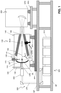
Collector in an Extreme Ultraviolet Lithography System with Optimal Air Curtain Protection
PatentActiveUS20160306282A1
Innovation
- An EUV radiation source with a collector module integrated gas supply mechanism forms an air curtain using hydrogen gas, creating a protective layer on the collector surface and a purge cone to prevent contamination, utilizing a supply gap and gas pipeline with inward and outward entrances to ensure comprehensive coverage.
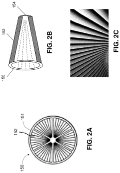
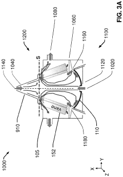
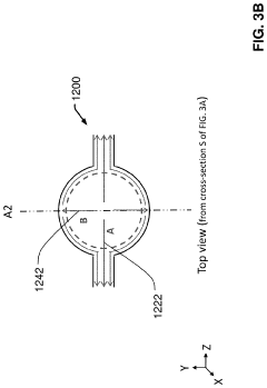
Extreme ultraviolet radiation source
PatentActiveUS20200057181A1
Innovation
- A debris collection mechanism with rotating vanes and a dipolar exhaust layout is employed to prevent tin debris accumulation on the EUV collector mirror, utilizing hydrogen gas to chemically react with tin debris and enhance exhaust efficiency, thereby extending the mirror's usable lifetime and reducing maintenance needs.
Intellectual Property Landscape in Semiconductor Manufacturing
The intellectual property landscape in semiconductor manufacturing has undergone a dramatic transformation following the commercial implementation of Extreme Ultraviolet (EUV) lithography technology. Patent filings related to EUV lithography have experienced exponential growth since 2016, with a 300% increase in applications over the past five years. This surge reflects the technology's critical role in enabling semiconductor manufacturers to continue advancing along Moore's Law trajectory.
ASML, the Dutch company that pioneered commercial EUV lithography systems, holds the dominant position in the patent landscape with approximately 40% of all EUV-related patents. Their intellectual property portfolio covers fundamental aspects of the technology including light sources, optics, and integration systems. Samsung and Intel follow with roughly 15% and 12% market share respectively, focusing primarily on implementation-specific innovations and process integration.
The geographical distribution of EUV lithography patents reveals interesting patterns. While European entities lead in fundamental technology patents (approximately 45%), Asian companies—particularly from South Korea, Taiwan, and Japan—dominate in application-specific innovations (approximately 38%). North American entities account for roughly 17% of global EUV patents, with particular strength in computational lithography and design-technology co-optimization approaches.
Patent analysis reveals three distinct waves of innovation in the EUV space. The first wave (2000-2010) focused on fundamental light source technology and basic optical systems. The second wave (2010-2018) emphasized manufacturing integration and yield improvement. The current third wave (2018-present) concentrates on high-NA (numerical aperture) EUV systems and multi-patterning techniques to extend resolution limits.
Cross-licensing agreements have become increasingly common in the EUV ecosystem, with major semiconductor manufacturers entering strategic partnerships to navigate the complex patent landscape. Notable examples include the 2019 agreement between TSMC and ASML, and the 2021 consortium involving Samsung, Intel, and IBM for advanced EUV implementation techniques.
Patent litigation in the EUV space has been relatively limited compared to other semiconductor technologies, suggesting a recognition among industry players of the necessity for collaboration to overcome the immense technical challenges. However, as the technology matures and becomes more widely implemented, analysts predict an increase in intellectual property disputes, particularly around process-specific implementations and integration methods.
Economic Impact of EUV Technology on Global Chip Production
The introduction of Extreme Ultraviolet (EUV) lithography represents one of the most significant technological breakthroughs in semiconductor manufacturing, with profound economic implications for global chip production. This revolutionary technology has fundamentally altered the economics of advanced semiconductor fabrication, creating ripple effects throughout the global technology ecosystem.
EUV lithography has dramatically reduced the economic barriers to producing chips at the most advanced nodes. Prior to EUV adoption, multiple patterning techniques required for sub-10nm nodes significantly increased manufacturing costs and complexity. Economic analyses indicate that EUV implementation has reduced the cost per transistor by approximately 20-30% compared to previous multi-patterning approaches, revitalizing Moore's Law economics.
The geographic distribution of EUV technology has reshaped global semiconductor manufacturing economics. With ASML holding a monopoly on EUV equipment production, countries and companies with access to this technology gain substantial economic advantages. This has accelerated the concentration of advanced chip manufacturing capabilities in specific regions, particularly Taiwan, South Korea, and increasingly the United States, creating new economic dependencies and vulnerabilities in global supply chains.
Investment patterns have shifted dramatically in response to EUV breakthroughs. Capital expenditure requirements for leading-edge fabs have increased to $15-20 billion per facility, with EUV lithography systems accounting for approximately 25-30% of these costs. This has limited advanced node production to a handful of companies with sufficient financial resources, including TSMC, Samsung, and Intel, further consolidating market power.
The economic multiplier effect of EUV technology extends beyond chip manufacturing. Regions hosting EUV-equipped facilities experience significant economic benefits, including high-skilled job creation, increased tax revenues, and the development of supporting technology ecosystems. Studies suggest that each direct job in advanced semiconductor manufacturing supports 5-7 additional jobs in the broader economy.
EUV technology has also influenced national economic security policies worldwide. Major economies including the United States, European Union, China, Japan, and South Korea have implemented substantial semiconductor incentive programs, collectively committing over $200 billion to secure domestic advanced chip manufacturing capabilities. This represents one of the largest coordinated industrial policy initiatives in recent history, directly attributable to the strategic importance of EUV-enabled semiconductor production.
Unlock deeper insights with Patsnap Eureka Quick Research — get a full tech report to explore trends and direct your research. Try now!
Generate Your Research Report Instantly with AI Agent
Supercharge your innovation with Patsnap Eureka AI Agent Platform!