

EUV Lithography: Impact Assessment on Consumer Electronics
OCT 14, 20259 MIN READ
Generate Your Research Report Instantly with AI Agent
PatSnap Eureka helps you evaluate technical feasibility & market potential.
EUV Lithography Evolution and Objectives
Extreme Ultraviolet (EUV) lithography represents a revolutionary advancement in semiconductor manufacturing technology, evolving from earlier lithography techniques that utilized deep ultraviolet (DUV) light sources. The journey began in the 1990s with initial research into EUV technology, but significant technical challenges delayed its commercial implementation until the late 2010s. This evolution was driven by the semiconductor industry's relentless pursuit of Moore's Law, which predicted the doubling of transistor density approximately every two years.
The primary objective of EUV lithography is to enable the production of increasingly smaller semiconductor components with higher precision and efficiency. With its 13.5nm wavelength—significantly shorter than the 193nm used in previous DUV systems—EUV technology allows for the creation of circuit patterns as small as 7nm and below, opening new frontiers in chip miniaturization and performance enhancement.
Throughout its development, EUV technology has overcome numerous technical hurdles, including the creation of suitable light sources, mirror systems, and photoresist materials capable of working with extreme ultraviolet light. The breakthrough came with the development of laser-produced plasma (LPP) sources that generate EUV light by firing laser pulses at droplets of molten tin, achieving the necessary power levels for commercial viability.
The evolution of EUV lithography has been marked by collaborative efforts across the semiconductor ecosystem, involving equipment manufacturers, chip designers, and research institutions. Companies like ASML, Intel, Samsung, and TSMC have invested billions in developing and refining this technology, recognizing its strategic importance for future electronic devices.
Looking forward, EUV lithography aims to continue pushing the boundaries of semiconductor manufacturing, with objectives including increased throughput, reduced defect rates, and adaptation for even smaller process nodes. The technology roadmap includes the development of high-numerical-aperture (high-NA) EUV systems, which promise to extend resolution capabilities to 3nm and beyond, potentially securing the continuation of Moore's Law for another decade.
For consumer electronics specifically, EUV lithography objectives include enabling the production of more powerful, energy-efficient processors and memory components that can support advanced applications such as artificial intelligence, augmented reality, and 5G connectivity in smartphones, tablets, and wearable devices. The technology also aims to facilitate the integration of more functionality into smaller form factors, driving innovation in product design and user experience.
Market Demand Analysis for Advanced Semiconductor Nodes
The semiconductor industry's demand for advanced nodes is primarily driven by the relentless pursuit of Moore's Law, which has historically guided the industry's trajectory toward smaller, faster, and more energy-efficient chips. Current market analysis indicates that the transition to sub-7nm nodes, enabled by EUV lithography, is accelerating due to explosive growth in data-intensive applications including artificial intelligence, 5G networks, and high-performance computing.
Consumer electronics represents the largest market segment driving demand for advanced semiconductor nodes. Smartphone manufacturers continue to push for more powerful processors in increasingly compact form factors, with premium devices now incorporating 5nm chips and planning rapid adoption of 3nm technology. This segment alone accounts for approximately 40% of advanced node semiconductor consumption, with annual growth rates exceeding 15% for cutting-edge nodes.
Computing devices constitute another significant market driver, with both personal computers and data center servers requiring increasingly powerful processors. The rise of AI-accelerated computing has created unprecedented demand for specialized chips manufactured on advanced nodes, as these applications benefit tremendously from the higher transistor densities and improved power efficiency. Cloud service providers are among the most aggressive adopters, with many placing substantial orders for 5nm and 3nm chips to power next-generation AI infrastructure.
Automotive electronics represents an emerging but rapidly growing market for advanced nodes. As vehicles incorporate more sophisticated driver assistance systems and autonomous driving capabilities, the computational requirements have increased exponentially. Premium electric vehicles now contain multiple advanced SoCs (Systems on Chip) manufactured at 7nm and below, with projections showing this segment growing at 25% annually through 2025.
The Internet of Things (IoT) presents a paradoxical market dynamic for advanced nodes. While many IoT applications prioritize cost over performance, the growing subset of edge computing devices requires significant processing power in energy-constrained environments – precisely the value proposition of advanced nodes. Industry analysts project that approximately 20% of IoT processors will utilize sub-10nm technology by 2025.
Supply constraints remain a significant factor affecting market dynamics. The limited availability of EUV lithography equipment, primarily supplied by ASML, has created production bottlenecks that impact pricing and availability. Current lead times for advanced node production capacity extend beyond 12 months, with premium pricing structures becoming standard practice among foundries. These constraints have prompted major consumer electronics manufacturers to secure long-term supply agreements and, in some cases, invest directly in semiconductor manufacturing capacity.
EUV Technology Status and Implementation Barriers
Extreme Ultraviolet (EUV) lithography represents a revolutionary advancement in semiconductor manufacturing, currently at varying stages of implementation across the global industry. Leading semiconductor manufacturers such as TSMC, Samsung, and Intel have begun integrating EUV technology into their high-volume manufacturing processes, primarily for nodes at 7nm and below. However, the adoption remains concentrated among these industry giants due to significant implementation barriers.
The foremost challenge in EUV implementation is the extraordinary capital expenditure required. A single EUV lithography system costs approximately $150-200 million, representing a substantial investment even for established manufacturers. This cost barrier effectively excludes smaller players from the market and concentrates advanced manufacturing capabilities among a few dominant companies.
Technical challenges continue to plague EUV implementation despite years of development. Power source stability remains problematic, with current EUV systems operating at around 250 watts—below the ideal 500-watt target for optimal throughput. This limitation directly impacts production efficiency and economic viability. Additionally, defectivity rates in EUV processes still exceed those of traditional lithography methods, requiring sophisticated defect detection and mitigation strategies.
Infrastructure requirements present another significant barrier. EUV systems demand specialized facilities with extraordinary environmental controls, including vibration isolation, temperature stability within ±0.05°C, and contamination-free environments. The physical footprint of these systems also necessitates purpose-built clean room facilities, adding to implementation costs.
The global supply chain for EUV technology presents both technical and geopolitical challenges. ASML maintains a near-monopoly on EUV lithography systems, creating a potential bottleneck in the semiconductor manufacturing ecosystem. Critical components such as specialized mirrors, photoresists, and masks have limited suppliers, introducing vulnerability to supply chain disruptions. Recent geopolitical tensions have further complicated access to this technology for certain regions.
Workforce development represents an often-overlooked barrier to EUV implementation. The technology requires highly specialized engineers and technicians with expertise in extreme ultraviolet physics, precision optics, and advanced process control. This talent pool remains limited globally, creating competition among manufacturers for qualified personnel and potentially delaying implementation timelines.
For consumer electronics specifically, these barriers translate to a bifurcated market where only premium devices benefit from the advantages of EUV-enabled chips in the near term. The concentration of EUV capabilities among few manufacturers may exacerbate supply constraints for advanced chips, potentially affecting product release cycles and pricing strategies across the consumer electronics industry.
Current EUV Implementation Solutions and Processes
01 EUV lithography system design and components
EUV lithography systems incorporate specialized components designed to work with extreme ultraviolet light. These systems typically include radiation sources, illumination optics, reticle stages, projection optics, and wafer stages. The design focuses on maintaining precise alignment and stability while operating in vacuum conditions required for EUV wavelengths. Advanced control systems manage thermal effects and vibration to ensure nanometer-level accuracy during exposure processes.- EUV lithography system design and components: EUV lithography systems incorporate specialized components designed to work with extreme ultraviolet light. These systems include illumination optics, projection optics, and reflective masks that operate in vacuum environments. The design focuses on achieving high resolution patterning while managing the challenges of working with short wavelength EUV radiation. Advanced optical elements and precise positioning mechanisms are essential for maintaining imaging accuracy at nanometer scales.
- Contamination control and mitigation in EUV systems: Contamination control is critical in EUV lithography due to the sensitivity of optical components to molecular and particulate contamination. Methods include specialized cleaning techniques, protective pellicles, gas purging systems, and contamination barriers. These approaches help prevent carbon growth on mirrors and masks, extend component lifetime, and maintain consistent imaging performance. Contamination mitigation strategies are essential for achieving economically viable operation of EUV lithography tools.
- EUV source technology and power optimization: EUV light sources typically use laser-produced plasma or discharge-produced plasma to generate the required 13.5nm wavelength radiation. Innovations focus on increasing source power, stability, and conversion efficiency while reducing debris generation. Advanced collector designs, fuel delivery systems, and plasma control mechanisms help maximize the usable EUV output. These developments are crucial for achieving the throughput requirements needed for high-volume manufacturing applications.
- Mask technology for EUV lithography: EUV masks are reflective rather than transmissive, consisting of multilayer mirrors with absorber patterns. Innovations include defect inspection and repair techniques, phase shifting structures, and mask pattern optimization. Advanced materials and manufacturing processes help minimize pattern distortions and maximize contrast. Mask handling systems protect these sensitive components from damage and contamination during storage and use in the lithography process.
- Thermal management and positioning control: Precise thermal management and positioning control are essential in EUV lithography systems due to the high energy densities involved and nanometer-scale precision requirements. Innovations include advanced cooling systems, thermal isolation techniques, and active temperature control. High-precision positioning systems with multi-axis control enable accurate alignment between the mask, wafer, and optical elements. These technologies help maintain imaging performance despite thermal loads from the intense EUV radiation.
02 EUV radiation sources and beam management
EUV lithography requires specialized radiation sources that can generate extreme ultraviolet light at approximately 13.5nm wavelength. These sources typically use laser-produced plasma or discharge-produced plasma technologies where high-energy lasers strike tin droplets or gas to create EUV radiation. The systems include sophisticated beam delivery, conditioning, and collection optics to maximize the usable EUV radiation while managing heat loads and contamination issues inherent to high-energy plasma generation.Expand Specific Solutions03 Mask technology and handling for EUV lithography
EUV masks (reticles) require specialized technology due to the reflective nature of EUV lithography. Unlike traditional transmissive photomasks, EUV masks consist of multilayer reflective coatings with absorber patterns on top. The handling systems must prevent contamination and defects while maintaining precise positioning. Advanced technologies include pellicle development to protect masks from particles, inspection systems to detect defects, and sophisticated mask stages that provide nanometer-level positioning accuracy during exposure.Expand Specific Solutions04 Contamination control and environmental management
EUV lithography systems require stringent contamination control due to the sensitivity of EUV optics and the vacuum environment. Technologies include hydrogen gas purging systems to prevent carbon contamination, specialized cleaning methods for optical surfaces, and particle management systems. Environmental control extends to temperature stabilization, vibration isolation, and electromagnetic shielding to maintain the precision required for sub-10nm feature patterning.Expand Specific Solutions05 Computational and process optimization for EUV lithography
Advanced computational methods enhance EUV lithography performance through sophisticated modeling, simulation, and process optimization. These include optical proximity correction algorithms tailored for EUV-specific effects, source mask optimization to improve pattern fidelity, and machine learning approaches to predict and compensate for process variations. Computational techniques also support the development of novel materials and processes specifically designed for the unique challenges of EUV lithography.Expand Specific Solutions
Key EUV Equipment Manufacturers and Chip Producers
EUV Lithography in consumer electronics is currently in a growth phase, with the market expanding rapidly due to increasing demand for advanced semiconductor chips. The technology has reached commercial maturity, with ASML Netherlands BV dominating as the sole supplier of EUV lithography systems. Key semiconductor manufacturers like Taiwan Semiconductor Manufacturing Co., Samsung Electronics, and Intel are driving adoption, investing billions in EUV technology to produce next-generation chips. The competitive landscape shows a clear stratification with ASML controlling the machine supply, while Carl Zeiss SMT provides critical optical components. Downstream, leading foundries compete for manufacturing excellence using this technology, creating a complex ecosystem where technological capabilities determine market position in producing smaller, more powerful consumer electronics.
Taiwan Semiconductor Manufacturing Co., Ltd.
Technical Solution: TSMC has pioneered the implementation of EUV lithography in high-volume manufacturing, being the first to mass produce 7nm and 5nm chips using this technology. Their approach integrates EUV into a comprehensive manufacturing process that includes multi-patterning techniques to achieve even greater precision than EUV alone would allow. TSMC's N5 process technology utilizes EUV for up to 14 critical layers, significantly reducing mask complexity compared to previous nodes. They've developed specialized photoresist materials optimized for EUV exposure characteristics and have created custom computational lithography models to maximize pattern fidelity. TSMC has also implemented innovative defect detection and correction methodologies specific to EUV processes. Their roadmap includes 3nm and 2nm nodes that will further expand EUV usage to more layers, enabling continued miniaturization of consumer electronics components. TSMC's implementation focuses on balancing performance, power efficiency, and cost considerations to make advanced nodes economically viable for consumer electronics applications.
Strengths: Industry-leading implementation expertise; proven high-volume manufacturing capability; strong relationships with consumer electronics companies; comprehensive process integration knowledge. Weaknesses: High capital expenditure requirements; geographic concentration risk; dependency on ASML for equipment; challenges in scaling to meet growing demand from multiple customers simultaneously.
ASML Netherlands BV
Technical Solution: ASML is the dominant player in EUV lithography technology, holding approximately 90% market share in the lithography equipment sector. Their NXE series EUV lithography systems, particularly the NXE:3600D, represent the cutting edge with resolution capabilities down to 13nm. This system operates at a wavelength of 13.5nm and utilizes a highly complex system of mirrors and reflective optics rather than traditional refractive lenses. ASML's technology incorporates a high-powered CO2 laser that creates plasma from tin droplets to generate EUV light. Their systems achieve throughput of over 160 wafers per hour, significantly improving production efficiency for advanced semiconductor nodes. ASML has also developed computational lithography solutions that enhance pattern fidelity and yield through sophisticated algorithms and simulation techniques. Their holistic approach includes not just the lithography equipment but also metrology and inspection systems to ensure quality control throughout the manufacturing process.
Strengths: Unmatched technical expertise in EUV systems; comprehensive ecosystem including software and services; strong IP portfolio with over 12,000 patents. Weaknesses: Extremely high cost of equipment (>$150 million per tool) creates barriers for smaller manufacturers; complex supply chain dependencies; limited production capacity causing delivery delays to customers.
Critical Patents and Innovations in EUV Technology
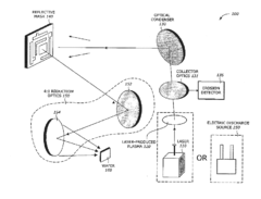
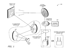
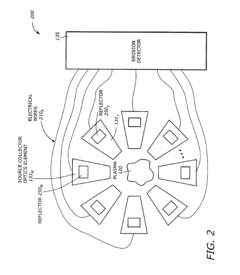
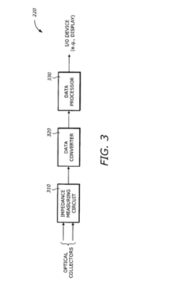
Detecting erosion in collector optics with plasma sources in extreme ultraviolet (EUV) lithography systems
PatentInactiveUS6841322B1
Innovation
- A system that detects erosion in the ML coating of EUVL stepper and optical systems by measuring initial and coating impedances over time, determining the erosion rate, and monitoring it in-situ to timely replace eroded collectors, using a combination of impedance measuring circuits, data converters, and data processors to initiate warnings and replacements.
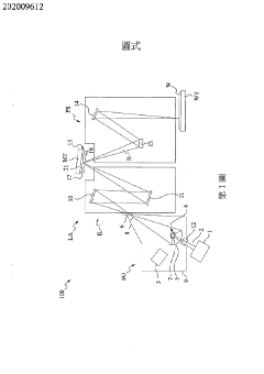
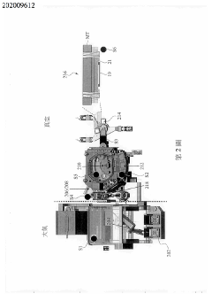
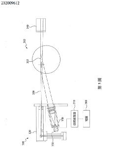
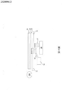
Extreme ultraviolet lithography system
PatentInactiveTW202009612A
Innovation
- Incorporation of sensors at various stages of the EUV lithography system to detect particle generation from membrane rupture, including particle counters, microphones, and acoustic wave sensors, allowing for early detection and localized contamination control.
Supply Chain Implications for Consumer Electronics
The integration of EUV lithography into semiconductor manufacturing processes has triggered profound transformations across the consumer electronics supply chain. Chip manufacturers adopting EUV technology have established new supplier relationships with specialized equipment providers, particularly ASML, which maintains a near-monopoly on EUV lithography systems. This concentration of critical technology in a single supplier creates both strategic advantages and potential vulnerabilities for downstream electronics manufacturers.
Supply chain reconfiguration has become inevitable as EUV adoption accelerates. Traditional semiconductor fabrication facilities require significant retrofitting or complete rebuilding to accommodate EUV systems, necessitating capital investments exceeding $1 billion per facility. This has prompted geographical shifts in manufacturing capabilities, with advanced node production increasingly concentrated in regions where companies can afford these substantial investments.
The component sourcing landscape for consumer electronics manufacturers has evolved dramatically. EUV-enabled chips offer superior performance characteristics but come with different availability timelines and cost structures. Procurement strategies now must account for longer lead times during initial production ramps and strategic partnerships with foundries possessing EUV capabilities have become essential competitive advantages for premium device manufacturers.
Inventory management practices have required significant adjustment to accommodate the new production realities of EUV lithography. The complex manufacturing process and high-value components necessitate more sophisticated forecasting models to prevent costly stockouts or overages. Consumer electronics companies must now maintain closer coordination with semiconductor suppliers to align production schedules with chip availability.
Risk mitigation has emerged as a critical supply chain consideration. The concentration of EUV expertise and equipment manufacturing creates potential bottlenecks that could impact the entire consumer electronics ecosystem. Forward-thinking companies have implemented multi-sourcing strategies where possible and developed contingency plans for potential disruptions in the EUV supply chain.
Cost implications ripple throughout the value chain, with EUV-produced chips commanding premium prices that must be absorbed or passed to consumers. This has accelerated market segmentation, with high-end consumer devices incorporating EUV-enabled components while budget offerings rely on chips manufactured using previous-generation lithography techniques. The resulting performance differential has become a key product differentiation factor in consumer electronics marketing.
Environmental and Energy Considerations of EUV Adoption
The adoption of Extreme Ultraviolet (EUV) lithography represents a significant technological advancement in semiconductor manufacturing, yet it brings substantial environmental and energy implications that warrant careful consideration. EUV systems consume extraordinary amounts of energy—approximately 1 megawatt per tool—significantly higher than previous generation Deep Ultraviolet (DUV) lithography equipment. This increased power demand stems primarily from the complex laser-produced plasma process required to generate EUV light, where high-powered CO2 lasers strike tin droplets to create the necessary 13.5nm wavelength radiation.
Water consumption presents another critical environmental concern. EUV systems require extensive cooling infrastructure, consuming thousands of gallons of ultra-pure water daily. This places considerable strain on local water resources, particularly in semiconductor manufacturing hubs that may already face water scarcity challenges. The purification processes for this water further compound the environmental footprint through additional energy consumption and chemical usage.
The production and operation of EUV systems also involve rare earth elements and specialized materials with complex supply chains and extraction processes that carry their own environmental burdens. The manufacturing of EUV equipment components—particularly the highly sophisticated mirrors with multi-layer coatings—requires energy-intensive precision manufacturing techniques and specialized materials processing.
From a lifecycle perspective, while EUV enables more efficient chip designs with potentially lower per-unit energy consumption, the environmental costs of implementation remain substantial. Industry estimates suggest that the carbon footprint associated with establishing EUV manufacturing capabilities at a single facility can be equivalent to tens of thousands of metric tons of CO2 emissions.
Several mitigation strategies are emerging within the industry. Leading manufacturers like ASML and their customers are investing in renewable energy infrastructure to offset the massive power requirements of EUV systems. Advanced heat recovery systems are being developed to capture and repurpose thermal energy from EUV operations. Water recycling technologies specifically designed for semiconductor manufacturing are advancing, with some facilities achieving over 90% water reuse rates.
The environmental equation becomes more nuanced when considering the end-user benefits. EUV-manufactured chips enable more energy-efficient consumer electronics, potentially offering lifecycle energy savings that could eventually offset the initial manufacturing impact. However, comprehensive lifecycle assessments that quantify these trade-offs remain limited, creating an important area for future research as EUV adoption accelerates across the consumer electronics supply chain.
Unlock deeper insights with PatSnap Eureka Quick Research — get a full tech report to explore trends and direct your research. Try now!
Generate Your Research Report Instantly with AI Agent
Supercharge your innovation with PatSnap Eureka AI Agent Platform!