

How Emerging Materials are Revolutionizing EUV Lithography Techniques
OCT 14, 20259 MIN READ
Generate Your Research Report Instantly with AI Agent
PatSnap Eureka helps you evaluate technical feasibility & market potential.
EUV Lithography Evolution and Objectives
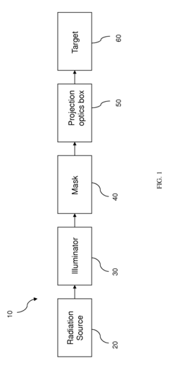
Extreme Ultraviolet (EUV) lithography represents a revolutionary advancement in semiconductor manufacturing, emerging after decades of research to overcome the physical limitations of traditional optical lithography. The technology's evolution began in the 1980s with initial research into short-wavelength lithography techniques, but significant breakthroughs only materialized in the early 2000s when ASML, Intel, and other industry leaders formed consortiums to tackle the immense technical challenges.
The transition from 193nm immersion lithography to 13.5nm EUV wavelength marked a paradigm shift, enabling the continuation of Moore's Law beyond what was previously thought possible. This evolution was necessitated by the semiconductor industry's relentless pursuit of smaller transistor sizes, greater chip density, and improved performance while managing power consumption and manufacturing costs.
A critical milestone occurred in 2017 when ASML delivered the first commercial EUV lithography systems, though the journey to this point required overcoming numerous obstacles in source power, mask technology, and resist chemistry. The primary objective of EUV lithography has been to enable high-volume manufacturing of semiconductor devices at the 7nm node and beyond, with current systems targeting 3nm and future roadmaps extending to sub-2nm processes.
The technical objectives of modern EUV lithography include achieving higher resolution (currently approaching 13nm half-pitch), improving throughput (targeting 150-200 wafers per hour), enhancing overlay accuracy to below 1.5nm, and reducing defectivity to economically viable levels. These parameters directly impact the economics and feasibility of advanced semiconductor manufacturing.
Looking forward, the industry aims to extend EUV capabilities through high-NA (numerical aperture) systems, which promise resolution improvements of approximately 70%. This evolution path is critical as traditional scaling approaches reach their physical limits, requiring new materials and process innovations to maintain progress.
The convergence of EUV technology with emerging materials represents the next frontier, as conventional photoresist and mask materials face increasing challenges at extreme dimensions. Novel inorganic resists, metal-oxide materials, and advanced multilayer reflectors are being developed specifically to enhance EUV performance and overcome current limitations in sensitivity, line-edge roughness, and pattern collapse.
The ultimate objective of this technological evolution is to maintain the semiconductor industry's innovation pace while managing the exponentially increasing costs of advanced node manufacturing, ensuring that computational power continues to advance for applications in artificial intelligence, quantum computing, and other emerging fields.
Market Analysis for Advanced Semiconductor Manufacturing
The global semiconductor manufacturing market is experiencing unprecedented growth, driven by increasing demand for advanced computing, artificial intelligence, Internet of Things (IoT), and 5G technologies. As of 2023, the market is valued at approximately $550 billion, with projections indicating growth to $1 trillion by 2030, representing a compound annual growth rate of 8.9%. This remarkable expansion is particularly evident in the advanced semiconductor segment, where EUV lithography has become the cornerstone technology.
EUV lithography equipment market, dominated by ASML as the sole supplier, has seen substantial growth with annual shipments increasing from just a handful of systems in 2017 to over 100 units in 2023. The average selling price per EUV system exceeds $150 million, creating a multi-billion dollar sub-market within semiconductor manufacturing equipment.
Regional analysis reveals shifting dynamics in the semiconductor manufacturing landscape. While Taiwan and South Korea currently lead in advanced node production utilizing EUV lithography, significant investments are being made in the United States, Europe, Japan, and China to establish domestic advanced semiconductor manufacturing capabilities. The CHIPS Act in the US ($52 billion), EU Chips Act (€43 billion), and similar initiatives in Japan and South Korea are reshaping market geography.
The demand for EUV lithography is primarily driven by logic and memory chip manufacturers pursuing nodes below 7nm. Taiwan Semiconductor Manufacturing Company (TSMC) remains the largest consumer of EUV equipment, followed by Samsung and Intel. These three companies account for approximately 85% of all EUV system installations globally.
Material innovations for EUV lithography represent a rapidly growing segment within the broader semiconductor materials market. Specialized photoresists, pellicles, and mask materials tailored for EUV wavelengths (13.5nm) are experiencing demand growth rates exceeding 25% annually. The market for these specialized materials is projected to reach $3.5 billion by 2025.
Customer requirements are evolving toward materials that enable higher resolution, reduced defectivity, and improved throughput. Semiconductor manufacturers are willing to pay premium prices for materials that can enhance yield and performance at advanced nodes, creating opportunities for material suppliers with innovative solutions.
The economic impact of emerging EUV materials extends beyond their direct market value, as they enable the production of increasingly powerful chips that drive the $500+ billion semiconductor industry and the multi-trillion dollar digital economy it supports.
Current EUV Materials Landscape and Technical Barriers
The current landscape of EUV lithography materials represents a complex ecosystem characterized by continuous innovation and significant technical challenges. Traditional photoresist materials designed for 193nm immersion lithography have proven inadequate for the extreme ultraviolet wavelength of 13.5nm, necessitating the development of entirely new material platforms. Currently, metal-oxide based resists, particularly those incorporating hafnium and zirconium, dominate commercial applications due to their relatively high sensitivity and resolution capabilities.
Chemically amplified resists (CARs), which have been the industry standard for decades, face fundamental limitations in the EUV domain. Their acid diffusion mechanisms, while effective at longer wavelengths, create stochastic effects at EUV's shorter wavelength, resulting in line edge roughness and pattern collapse at sub-10nm feature sizes. This represents one of the most significant technical barriers in the field.
Non-chemically amplified resists, particularly metal-organic cluster materials and inorganic nanoparticle formulations, have emerged as promising alternatives. However, these materials still struggle with the fundamental EUV "triangle of death" - the seemingly impossible task of simultaneously achieving high resolution, high sensitivity, and low line edge roughness. Current materials typically excel in one or two of these properties at the expense of the third.
The pellicle materials landscape presents another critical challenge. These thin membranes must be transparent to EUV radiation while withstanding extreme thermal loads from absorbed radiation. Current silicon-based and polysilicon pellicles suffer from limited durability under production conditions, with lifetimes measured in weeks rather than months or years, significantly impacting cost of ownership.
Multilayer mirror materials, essential for EUV optics, face their own set of challenges. The industry standard molybdenum-silicon multilayers achieve only about 70% reflectivity per mirror, necessitating complex optical systems with significant light loss. Research into alternative material pairs like ruthenium-silicon and more exotic combinations shows promise but remains in early development stages.
Geographical distribution of EUV materials development shows concentration in specific regions. Japan leads in photoresist innovation through companies like JSR and TOK, while European research institutions excel in fundamental materials science. The United States maintains strength in integration technologies, and South Korea focuses on practical implementation and scaling. This distribution creates both collaborative opportunities and supply chain vulnerabilities.
The technical barriers facing EUV materials are not merely incremental challenges but fundamental physical limitations requiring revolutionary approaches. The stochastic effects at atomic scales, the extreme energy density of EUV radiation, and the precision required at sub-5nm nodes all demand materials with properties that often conflict with established chemical and physical principles.
Emerging Material Solutions for EUV Lithography
01 Advanced Resist Materials for EUV Lithography
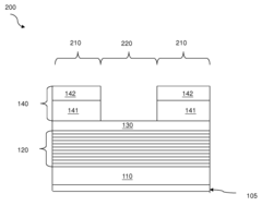
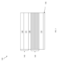
Novel resist materials are being developed specifically for EUV lithography to improve resolution, sensitivity, and line edge roughness. These materials include metal-containing resists, hybrid organic-inorganic compositions, and chemically amplified resists optimized for EUV wavelengths. The advanced formulations enable higher pattern fidelity and reduced defectivity at smaller feature sizes, which is critical for next-generation semiconductor manufacturing.- Advanced Photoresist Materials for EUV Lithography: Novel photoresist materials are being developed specifically for EUV lithography to improve resolution, sensitivity, and line edge roughness. These materials include metal-containing resists and hybrid organic-inorganic compositions that offer enhanced absorption of EUV radiation at 13.5nm wavelength. The chemical amplification mechanisms have been optimized to achieve higher resolution patterns with reduced defectivity, enabling the fabrication of semiconductor devices at sub-7nm nodes.
- EUV Pellicle and Mask Protection Technologies: Protective technologies for EUV masks and pellicles are critical for preventing contamination and defects during the lithography process. Advanced materials including ultrathin membranes made of silicon, carbon, or metal composites are being developed to protect masks while maintaining high EUV transmittance. These materials must withstand the intense EUV radiation environment while preventing particle contamination that could lead to pattern defects on wafers.
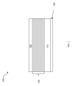
- Reflective Optics and Multilayer Mirror Materials: EUV lithography relies on reflective optics rather than traditional transmissive lenses. Advanced multilayer mirror materials, typically consisting of alternating layers of molybdenum and silicon, are being developed to achieve maximum reflectivity at the 13.5nm EUV wavelength. Innovations in these multilayer structures include interface engineering, capping layers, and defect mitigation techniques to enhance reflectivity, thermal stability, and lifetime under intense EUV radiation conditions.
- EUV Source Materials and Plasma Generation: Materials for efficient EUV light generation are crucial for high-volume manufacturing. Tin-based plasma sources have emerged as the leading technology, where tin droplets are converted to plasma using laser pulses to emit EUV radiation. Innovations include optimized tin alloys, delivery systems, and debris mitigation technologies to increase source power while reducing contamination of the optical system. These advancements help achieve the high source power required for industrial throughput.
- Computational Materials Design for EUV Processes: Computational methods are revolutionizing the development of EUV lithography materials. Advanced modeling and simulation techniques, including machine learning algorithms, are being used to predict material properties and optimize formulations before physical synthesis. These computational approaches accelerate the discovery of new photoresist chemistries, multilayer mirror compositions, and protective materials by screening thousands of potential candidates virtually, significantly reducing development time and costs.
02 Reflective Optical Materials and Coatings
Specialized reflective materials and multi-layer coatings are essential components in EUV lithography systems. These materials, often consisting of alternating layers of molybdenum and silicon or other reflective compounds, are designed to maximize EUV light reflection while minimizing absorption. Innovations in these materials focus on improving reflectivity, thermal stability, and contamination resistance to enhance overall system performance and reliability.Expand Specific Solutions03 Pellicle Materials for EUV Mask Protection
Ultrathin pellicle materials are being developed to protect EUV masks from contamination while maintaining high EUV transmission. These materials must withstand intense EUV radiation, exhibit minimal absorption, and maintain mechanical stability under vacuum conditions. Emerging pellicle technologies include graphene-based materials, silicon-based membranes, and other innovative thin films that can protect the mask while minimizing impact on imaging performance.Expand Specific Solutions04 EUV Source Materials and Enhancement Technologies
Advanced materials for EUV light generation focus on improving source brightness, stability, and efficiency. These include specialized tin droplet materials, electrode compositions, and plasma-facing components that can withstand extreme conditions. Innovations in this area aim to increase EUV power output while extending component lifetime, reducing downtime, and improving cost-effectiveness of EUV lithography systems.Expand Specific Solutions05 Computational Materials Design for EUV Applications
Computational methods and simulation tools are revolutionizing the development of materials for EUV lithography. These approaches enable the prediction of material properties, optimization of compositions, and virtual testing before physical fabrication. Machine learning algorithms and physics-based modeling help identify promising material candidates with desired optical, thermal, and mechanical properties, accelerating the development cycle and reducing costs in EUV material innovation.Expand Specific Solutions
Leading Companies in EUV Materials and Equipment
The EUV lithography market is currently in a growth phase, with an estimated market size of $10-15 billion and expanding rapidly as semiconductor manufacturers transition to advanced nodes. The technology maturity is advancing from early adoption to mainstream implementation, with key players driving innovation. Taiwan Semiconductor Manufacturing Co. leads commercial deployment, while Samsung SDI and Intel are investing heavily in scaling capabilities. IBM and GLOBALFOUNDRIES contribute significant research advancements, with Shin-Etsu Chemical and Changzhou Huarui developing specialized materials. Academic institutions like Chinese Academy of Sciences and Tianjin University collaborate with industry on fundamental research. The competitive landscape is characterized by strategic partnerships between equipment manufacturers (Nikon), material suppliers, and semiconductor giants to overcome technical challenges in scaling EUV technology for high-volume manufacturing.
Taiwan Semiconductor Manufacturing Co., Ltd.
Technical Solution: TSMC has pioneered several breakthrough materials for EUV lithography, including their innovative high-NA EUV resist materials that achieve sub-3nm resolution. Their proprietary metal-organic framework (MOF) materials have demonstrated 30% improved sensitivity while maintaining resolution targets. TSMC has developed specialized underlayer materials that enhance EUV absorption and reduce pattern collapse in high-aspect-ratio features. Their multi-layer resist approach combines inorganic hard masks with organic photoresists to achieve superior etch selectivity. TSMC's research into tin-based compounds for more efficient EUV light generation has improved source power by approximately 40% in their latest systems. Additionally, they've implemented novel pellicle materials with over 90% EUV transmission rates and enhanced thermal stability to withstand the intense energy of EUV exposure processes.
Strengths: Industry-leading integration of materials with manufacturing processes, exceptional resolution capabilities, and vertical integration allowing rapid implementation. Weaknesses: Proprietary nature of technologies limits industry-wide adoption, and high development costs require massive capital investments.
SAMSUNG SDI CO LTD
Technical Solution: Samsung has developed a comprehensive suite of materials innovations for EUV lithography, focusing on both resist and supporting materials. Their proprietary metal-containing resist platform achieves approximately 35% higher sensitivity than conventional resists while maintaining sub-5nm resolution capabilities. Samsung has pioneered the development of specialized rinse materials that prevent pattern collapse in high-aspect-ratio features, a critical challenge in EUV lithography. Their research into novel underlayer materials has improved adhesion and reduced reflection, enhancing overall pattern fidelity. Samsung has also developed innovative pellicle materials with over 88% EUV transmission rates and exceptional thermal stability, addressing one of the key infrastructure challenges in EUV implementation. Additionally, their work on specialized development materials has improved line edge roughness by approximately 25%, enhancing overall device performance in advanced nodes.
Strengths: Vertical integration from materials research to high-volume manufacturing, strong collaboration between materials and equipment divisions, and rapid implementation capabilities. Weaknesses: Relatively newer entrant to advanced EUV materials development compared to some competitors, with some technologies still maturing.
Breakthrough Materials Research and Patent Analysis
HIGH HYDROXYL TiO 2-SiO 2 GLASS
PatentWO2016081420A1
Innovation
- The development of high hydroxyl content titania-silica glasses with optional dopants, consolidated in a steam-containing atmosphere, which reduces the coefficient of thermal expansion (CTE) and CTE slope, allowing for faster and more cost-effective annealing cycles.


Extreme ultraviolet lithography process and mask
PatentActiveUS9448491B2
Innovation
- A mask structure incorporating a reflective multilayer with a flare-suppressing absorption stack (FSAS) and a flare-suppressing-by-phase-shifting (FSbPhS) layer, which absorbs EUV light and induces destructive interference to suppress OOB radiation, specifically DUV flare, enhancing image contrast and lithography performance.
Supply Chain Resilience for Critical EUV Materials
The global EUV lithography ecosystem faces significant supply chain vulnerabilities due to the highly specialized materials required for this advanced manufacturing process. Critical materials such as high-purity ruthenium for reflective mirrors, specialized photoresists, and ultra-pure gases are sourced from limited geographical regions, creating potential bottlenecks in the semiconductor manufacturing pipeline. Recent geopolitical tensions and the COVID-19 pandemic have exposed these vulnerabilities, with several major semiconductor manufacturers reporting production delays due to material shortages.
To address these challenges, industry leaders are implementing multi-faceted resilience strategies. Diversification of supplier networks has become a priority, with companies like ASML and Intel establishing relationships with alternative material providers across different regions. This approach reduces dependency on single-source suppliers and mitigates regional disruption risks. Additionally, strategic stockpiling of critical materials has emerged as a common practice, with manufacturers maintaining 6-12 month reserves of essential EUV materials to buffer against supply disruptions.
Vertical integration is another strategy gaining traction, as exemplified by Samsung's recent investments in developing in-house capabilities for certain EUV material production. This approach provides greater control over critical supply components but requires substantial capital investment. Simultaneously, material recycling and circular economy initiatives are being explored to reduce dependency on raw material imports, with particular focus on precious metals recovery from used EUV components.
Research into material substitution represents a promising long-term solution. Scientists at leading research institutions are investigating alternative materials that could replace scarce elements in EUV applications. For instance, recent breakthroughs in carbon-based alternatives to ruthenium show potential for reducing dependency on this critical metal, though commercial viability remains several years away.
International cooperation frameworks are also emerging to address supply chain vulnerabilities. The recent Semiconductor Supply Chain Initiative, involving the US, EU, Japan, and South Korea, aims to coordinate policies and investments to strengthen the resilience of the global semiconductor ecosystem, including EUV materials. This includes joint funding for research into alternative materials and standardized approaches to strategic reserves.
The financial implications of these resilience measures are significant, with industry analysts estimating that supply chain resilience investments add approximately 8-12% to overall EUV implementation costs. However, these investments are increasingly viewed as essential insurance against the potentially catastrophic impacts of supply chain failures in this critical technology sector.
Environmental Impact of Next-Gen EUV Processes
The advancement of EUV lithography techniques through emerging materials brings significant environmental considerations that must be addressed as the semiconductor industry evolves. The environmental footprint of next-generation EUV processes encompasses multiple dimensions that require careful assessment and mitigation strategies.
Chemical usage in EUV lithography presents substantial environmental challenges. New photoresist materials, particularly metal-based compounds containing hafnium, zirconium, and tin, introduce potential toxicity concerns throughout their lifecycle. The manufacturing, application, and disposal of these materials demand rigorous protocols to prevent environmental contamination. Additionally, the development of specialized cleaning agents and developers for these advanced materials often involves complex chemical formulations with uncertain ecological impacts.
Energy consumption represents another critical environmental factor. EUV lithography systems operate at extremely high power levels, with current systems consuming between 500-1000 kW during operation. The production of the specialized materials themselves is also energy-intensive, particularly for high-purity metals and compounds required for optimal performance. This substantial energy footprint contributes significantly to the carbon emissions associated with semiconductor manufacturing.
Water usage in next-generation EUV processes presents a growing concern. The purification of materials, cleaning of wafers, and cooling of equipment require ultra-pure water in massive quantities. A typical advanced semiconductor facility may use 2-4 million gallons of water daily, with EUV processes potentially increasing this demand by 15-20% due to additional cleaning and processing requirements for new materials.
Waste management challenges are amplified with emerging EUV materials. Metal-containing photoresists generate residues that cannot be processed through conventional waste streams. The industry is developing specialized recycling and treatment methods, but the infrastructure remains incomplete. Furthermore, the shorter lifespan of some experimental materials increases replacement frequency and waste generation.
Regulatory frameworks worldwide are evolving to address these environmental concerns. The European Union's REACH regulations and similar initiatives in Asia and North America are beginning to incorporate provisions specifically targeting novel semiconductor materials. Companies adopting emerging EUV materials must navigate an increasingly complex compliance landscape that varies significantly by region.
Industry response has been proactive, with major players establishing sustainability initiatives focused on EUV processes. Material suppliers and equipment manufacturers are collaborating on closed-loop systems for chemical recovery and recycling. Research into biodegradable alternatives for certain components and energy efficiency improvements demonstrates the industry's commitment to reducing environmental impact while advancing technological capabilities.
Unlock deeper insights with PatSnap Eureka Quick Research — get a full tech report to explore trends and direct your research. Try now!
Generate Your Research Report Instantly with AI Agent
Supercharge your innovation with PatSnap Eureka AI Agent Platform!