EUV Lithography: A Detailed Analysis of Cost-Effectiveness and ROI
OCT 14, 20259 MIN READ
Generate Your Research Report Instantly with AI Agent
Patsnap Eureka helps you evaluate technical feasibility & market potential.
EUV Lithography Evolution and Objectives
Extreme Ultraviolet (EUV) lithography represents a revolutionary advancement in semiconductor manufacturing technology, marking a significant departure from traditional Deep Ultraviolet (DUV) lithography methods. The evolution of EUV technology spans over three decades, beginning in the 1980s with initial research into short-wavelength lithography techniques. By the 1990s, EUV emerged as a promising candidate for next-generation lithography, with wavelengths of 13.5nm offering the potential to create significantly smaller circuit patterns than the 193nm wavelength used in DUV systems.
The development trajectory accelerated in the early 2000s when industry consortiums like ASML, Intel, and Samsung began substantial investments in EUV research. However, numerous technical challenges, including source power limitations, mask defects, and resist performance issues, delayed commercial implementation for nearly two decades. The first production-ready EUV lithography systems were only introduced by ASML in 2017, with volume manufacturing beginning around 2019.
This protracted development timeline reflects the immense technical complexity involved in creating a viable EUV ecosystem. The technology requires fundamentally different approaches to nearly every aspect of the lithography process, from light sources utilizing laser-produced plasma to specialized vacuum environments and entirely new mask and resist technologies.
The primary objective of EUV lithography is to enable semiconductor manufacturers to continue following Moore's Law by producing increasingly smaller transistors at economically viable costs. Specifically, EUV aims to facilitate high-volume manufacturing of semiconductor devices at the 7nm node and beyond, where traditional DUV lithography faces insurmountable physical limitations or requires prohibitively complex multi-patterning techniques.
Secondary objectives include improving yield rates for advanced nodes, reducing the number of process steps required for complex patterns, and ultimately lowering the per-transistor cost of semiconductor manufacturing. These objectives directly address the economic challenges of continuing semiconductor scaling, as traditional lithography approaches face diminishing returns in terms of cost-effectiveness at advanced nodes.
Looking forward, the technology roadmap for EUV includes the development of high-numerical-aperture (high-NA) EUV systems, which promise to extend resolution capabilities even further. Additionally, ongoing research focuses on improving source power, reducing defectivity, and enhancing overall system reliability to maximize return on investment for semiconductor manufacturers who have committed to this technology path.
Semiconductor Industry Demand Analysis
The semiconductor industry's demand for advanced lithography technologies, particularly EUV (Extreme Ultraviolet) lithography, has been growing exponentially in recent years. This growth is primarily driven by the continuous miniaturization of semiconductor devices and the industry's pursuit of Moore's Law, which predicts the doubling of transistor density approximately every two years. As node sizes shrink below 7nm, traditional DUV (Deep Ultraviolet) lithography faces significant challenges in achieving the required resolution, making EUV technology increasingly essential.
Market analysis indicates that the global semiconductor industry is projected to reach $1 trillion by 2030, with advanced nodes requiring EUV technology representing a significant portion of this market. The demand is particularly strong in high-performance computing, artificial intelligence, 5G infrastructure, and autonomous driving applications, where chip performance and power efficiency are critical competitive factors.
Leading semiconductor manufacturers, including TSMC, Samsung, and Intel, have committed substantial investments to EUV-based manufacturing processes. TSMC alone has ordered multiple EUV systems for its 5nm and 3nm production lines, with each system costing approximately $150 million. This significant capital expenditure underscores the industry's confidence in EUV technology as a critical enabler for future semiconductor manufacturing.
The demand for EUV lithography is further amplified by the increasing complexity of chip designs and the growing need for multi-patterning techniques at advanced nodes. While EUV technology reduces the number of process steps compared to multiple patterning with DUV, the initial investment and operational costs remain substantial challenges for manufacturers.
Regional analysis reveals that East Asia dominates the demand for EUV lithography systems, with Taiwan, South Korea, and increasingly China being the primary markets. North America and Europe also maintain significant demand, primarily driven by Intel and research institutions focused on advancing semiconductor manufacturing capabilities.
The COVID-19 pandemic and subsequent global chip shortage have highlighted the strategic importance of semiconductor manufacturing capacity, prompting governments worldwide to invest in domestic semiconductor production capabilities. This trend is expected to further increase the demand for advanced lithography technologies, including EUV, as countries seek technological sovereignty in critical semiconductor manufacturing.
Despite the high costs associated with EUV lithography, the technology's ability to enable continued scaling and performance improvements makes it indispensable for leading-edge semiconductor manufacturing. The industry's willingness to bear these costs reflects the critical nature of lithography in maintaining competitive advantage in the semiconductor market.
Global EUV Technology Status and Barriers
Extreme Ultraviolet (EUV) lithography represents a significant technological breakthrough in semiconductor manufacturing, yet its global implementation faces substantial challenges. Currently, ASML of the Netherlands holds a monopoly on EUV lithography systems, with their NXE series machines being the only commercially viable option. This market concentration creates both technological and geopolitical barriers for widespread adoption.
The primary technical barrier remains the complexity of the EUV light source. Generating and maintaining stable 13.5nm wavelength light requires sophisticated laser-produced plasma systems using tin droplets, which demand extraordinary precision engineering. The optical systems, particularly the multilayer mirrors that replace traditional lenses, present another significant challenge as they must maintain atomic-level accuracy while handling extreme thermal loads.
Cost barriers are equally prohibitive. A single EUV lithography system costs approximately $150-200 million, with additional infrastructure requirements pushing total implementation costs beyond $300 million per unit. This represents a capital expenditure that only the largest semiconductor manufacturers can justify, creating a significant entry barrier for smaller players and developing economies.
Operational challenges further complicate global adoption. EUV systems require specialized facilities with extraordinary cleanliness standards, vibration isolation, and temperature control. The power consumption exceeds 1MW per system, necessitating substantial energy infrastructure. Additionally, the maintenance complexity and specialized knowledge required for operation create workforce barriers in regions without established semiconductor expertise.
Supply chain vulnerabilities constitute another critical barrier. Key components for EUV systems come from a limited number of suppliers across Europe, North America, and Asia. This concentration creates bottlenecks that have been exacerbated by recent global supply chain disruptions, limiting production capacity to approximately 35-40 systems annually.
Intellectual property restrictions present significant barriers to technology transfer. ASML's EUV technology incorporates over 2,000 patents, while export controls from the Netherlands, Japan, and the United States restrict the sale of these systems to certain countries, creating geopolitical barriers to technology access.
Despite these challenges, EUV adoption continues to grow among leading semiconductor manufacturers. TSMC, Samsung, and Intel have all made substantial investments in EUV technology, recognizing its necessity for advancing to 5nm nodes and beyond. However, the technology remains concentrated in a handful of advanced facilities in Taiwan, South Korea, the United States, and Japan, highlighting the significant gap between leading-edge capabilities and the broader semiconductor manufacturing landscape.
Current EUV Implementation Strategies
01 Cost-effectiveness analysis of EUV lithography systems
EUV lithography systems represent significant capital investments for semiconductor manufacturers. Cost-effectiveness analysis involves evaluating the total cost of ownership, including initial equipment costs, operational expenses, and maintenance requirements. These systems can provide economic benefits through higher throughput, reduced process steps, and improved yield rates compared to traditional lithography methods. The return on investment is typically calculated based on production volume capabilities and the ability to manufacture advanced node semiconductors that command premium pricing.- Cost-effectiveness of EUV lithography systems: EUV lithography systems represent significant capital investments for semiconductor manufacturers. The cost-effectiveness analysis includes considerations of initial equipment costs, operational expenses, and throughput capabilities. Despite high initial costs, EUV lithography can be economically viable for high-volume manufacturing of advanced semiconductor nodes due to reduced process steps compared to multiple patterning techniques, leading to potential long-term cost savings and improved yield rates.
- Throughput optimization for ROI improvement: Maximizing the return on investment for EUV lithography systems requires optimizing throughput parameters. This includes enhancing source power, improving resist sensitivity, reducing overhead time, and implementing efficient wafer handling systems. Advanced control algorithms and system designs that minimize downtime and maximize wafer processing capacity directly impact the economic viability of EUV technology in production environments.
- Maintenance costs and system reliability: The reliability of EUV lithography systems significantly impacts their cost-effectiveness. Maintenance requirements, including mirror degradation, contamination control, and vacuum system upkeep, contribute substantially to operational expenses. Innovations in system design that extend component lifetimes, reduce maintenance frequency, and enable predictive maintenance capabilities help improve the overall return on investment by minimizing production interruptions and extending equipment useful life.
- Process integration and yield considerations: The economic viability of EUV lithography depends on successful process integration and yield management. This includes optimizing resist chemistry, developing effective pattern transfer processes, and implementing defect reduction strategies. Higher yields directly improve cost-effectiveness by reducing waste and rework. Advanced metrology and inspection techniques that enable rapid process optimization and defect identification contribute significantly to achieving favorable return on investment metrics.
- Multi-generational equipment strategies: Semiconductor manufacturers can improve EUV lithography ROI through strategic equipment deployment across multiple technology generations. This includes designing systems with upgrade paths, implementing field-retrofittable components, and planning for technology transitions. By extending the useful life of EUV equipment across multiple product generations and ensuring compatibility with evolving manufacturing requirements, companies can amortize the high initial investment costs over longer periods and improve overall return on investment.
02 Throughput optimization for ROI improvement
Maximizing the throughput of EUV lithography systems is crucial for achieving favorable return on investment. This involves optimizing exposure times, wafer handling processes, and system uptime. Advanced control systems can reduce idle time between exposures and improve overall equipment effectiveness. Innovations in source power, optical systems, and stage movement contribute to higher wafer throughput rates. These optimizations directly impact the cost per wafer and ultimately the economic viability of EUV technology for various semiconductor applications.Expand Specific Solutions03 Maintenance cost reduction strategies
Maintenance costs represent a significant portion of the total cost of ownership for EUV lithography systems. Strategies to reduce these costs include developing more durable components, implementing predictive maintenance systems, and designing for easier serviceability. Advanced monitoring systems can detect potential failures before they occur, reducing unplanned downtime. Extending the lifetime of critical components such as mirrors, masks, and light sources can significantly improve the return on investment by reducing replacement frequency and associated costs.Expand Specific Solutions04 Multi-patterning versus EUV economic comparison
Economic comparisons between traditional multi-patterning techniques and EUV lithography are essential for ROI analysis. While EUV systems require higher initial investment, they can reduce the number of process steps needed for advanced nodes compared to multi-patterning approaches. This reduction in process complexity can lead to lower overall manufacturing costs, improved yield, and faster time-to-market for new semiconductor products. The economic crossover point where EUV becomes more cost-effective than multi-patterning depends on factors such as production volume, feature density, and required resolution.Expand Specific Solutions05 Integration with existing manufacturing infrastructure
The cost-effectiveness of EUV lithography is influenced by how well it integrates with existing semiconductor manufacturing infrastructure. Compatibility with established workflows, equipment, and materials can significantly reduce implementation costs. Hybrid approaches that strategically deploy EUV for critical layers while using conventional lithography for less demanding features can optimize the overall return on investment. Factory automation systems and integrated metrology solutions further enhance the economic benefits by improving process control and reducing the need for separate inspection steps.Expand Specific Solutions
Leading EUV Equipment Manufacturers and Adopters
EUV Lithography is currently in the growth phase, with a rapidly expanding market expected to reach $10 billion by 2025. The technology has matured significantly but remains concentrated among few players. ASML Netherlands BV dominates as the sole EUV lithography system manufacturer, while Taiwan Semiconductor Manufacturing Co. (TSMC), Intel, and Samsung are leading adopters. GlobalFoundries and SMIC are working to catch up in implementation. Supporting ecosystem players include Nikon, Tokyo Electron, and AGC providing specialized materials and components. The cost-effectiveness analysis reveals significant ROI despite high initial investment ($120-150 million per tool), as EUV enables advanced node production with fewer process steps and higher yields compared to traditional multi-patterning approaches.
Taiwan Semiconductor Manufacturing Co., Ltd.
Technical Solution: TSMC has pioneered the commercial implementation of EUV lithography, deploying it first in their 7nm+ process and extensively in their 5nm and 3nm nodes. Their EUV strategy focuses on maximizing return on investment through high utilization rates and yield optimization. TSMC has developed a comprehensive EUV infrastructure including specialized clean rooms, advanced mask handling systems, and proprietary process recipes that maximize the technology's cost-effectiveness. Their approach includes strategic layer selection, applying EUV only to critical dimensions where it provides maximum economic benefit while using immersion lithography for less demanding layers. TSMC's internal data indicates their EUV implementation reduces mask counts by approximately 30-40% for advanced nodes compared to multiple patterning alternatives, significantly lowering manufacturing complexity and cycle time. They've also developed specialized metrology and inspection techniques for EUV-specific defects, achieving yield improvements that further enhance ROI. TSMC's scale allows them to amortize the high capital costs of EUV equipment across massive production volumes, with reports suggesting they achieve full ROI on EUV tools within 3-4 years of deployment.
Strengths: First-mover advantage in commercial EUV deployment; massive production scale allowing cost amortization; proven expertise in yield management for EUV processes. Weaknesses: Heavy dependence on ASML as sole EUV equipment supplier; high capital expenditure requirements for maintaining technology leadership; vulnerability to geopolitical risks affecting equipment access.
Intel Corp.
Technical Solution: Intel has developed a comprehensive EUV implementation strategy focused on optimizing cost-effectiveness through a "co-optimization" approach. Their technique involves simultaneous development of design rules, process technologies, and EUV-specific circuit architectures to maximize return on their substantial EUV investment. Intel's approach includes proprietary computational lithography solutions that enhance EUV pattern fidelity while reducing mask complexity and cost. For their 7nm (Intel 4) and 5nm (Intel 3) nodes, they've implemented a hybrid lithography strategy that strategically deploys EUV only for critical layers where it delivers maximum economic benefit, while using established immersion lithography for less demanding layers. Intel has also invested in specialized resist materials and mask infrastructure to improve EUV yield and throughput. Their internal analysis shows that despite EUV's high capital costs, the technology reduces overall process complexity by eliminating multiple patterning steps, resulting in 20-30% cost savings for advanced nodes when total manufacturing costs are considered.
Strengths: Vertical integration allowing for customized EUV implementation; strong computational lithography capabilities; ability to optimize chip designs specifically for EUV process characteristics. Weaknesses: Later adoption of EUV compared to competitors like TSMC; higher initial implementation costs due to retrofitting existing fabs rather than building new EUV-optimized facilities.
Critical Patents and Technical Breakthroughs
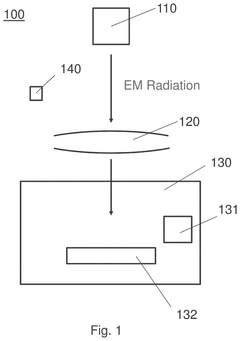
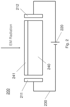
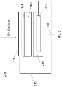
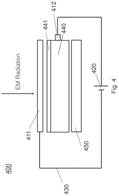
Methods and systems for electric field-assisted lithography
PatentPendingUS20250085639A1
Innovation
- The system comprises an electromagnetic radiation source, an optical assembly, and an exposure chamber with a substrate support and an electrode assembly that applies an electric field to an EM-sensitive layer on the semiconductor substrate during exposure to EUV radiation.
Cost-Benefit Analysis and ROI Metrics
The economic implications of EUV lithography adoption represent a critical consideration for semiconductor manufacturers. Initial investment costs for EUV technology are substantial, with each lithography system priced between $120-150 million, significantly higher than traditional DUV systems at $40-60 million. Additionally, installation and facility preparation can add $20-30 million per system, creating a considerable capital expenditure barrier.
Operating costs further impact the financial equation, with EUV systems consuming approximately 40% more power than their DUV counterparts. Maintenance expenses are estimated at 5-7% of the initial system cost annually, translating to $6-10 million per year per system. Mask costs for EUV technology also exceed traditional alternatives by 30-40%.
Despite these elevated costs, quantifiable benefits emerge when analyzing throughput and yield improvements. EUV technology reduces multi-patterning requirements, decreasing process steps by 20-30% for advanced nodes. This streamlining results in cycle time reductions of 15-25% and yield improvements of 3-5% at mature production levels, directly impacting production economics.
Return on investment calculations indicate that most semiconductor manufacturers achieve breakeven on EUV investments within 3-5 years, depending on production volume and node specifications. High-volume manufacturers producing premium chips typically realize faster ROI, while those with lower volumes face extended payback periods. Industry data suggests that for 5nm node production, the cost-per-transistor reduction enabled by EUV technology ranges from 15-20% compared to multi-patterning DUV approaches.
Risk-adjusted ROI models incorporating factors such as market demand fluctuations, technology maturation rates, and competitive positioning demonstrate that early EUV adopters gained significant competitive advantages despite higher initial risks. These advantages manifest as earlier time-to-market for advanced node products and enhanced ability to secure premium customers requiring cutting-edge process technologies.
Long-term economic analysis reveals that while initial EUV implementation presents substantial financial challenges, the technology becomes increasingly cost-effective with each subsequent node advancement. The economic inflection point typically occurs at the 7nm/5nm transition, where the complexity of multi-patterning alternatives begins to outweigh EUV implementation costs. This trend accelerates at 3nm and beyond, where EUV becomes the only economically viable option for critical layers.
Supply Chain Resilience and Geopolitical Factors
The EUV lithography supply chain represents a critical vulnerability in the semiconductor industry due to its highly concentrated nature. ASML, based in the Netherlands, maintains a near-monopoly on EUV lithography systems, creating a single point of failure in the global semiconductor manufacturing ecosystem. This concentration of essential technology has elevated EUV lithography to a geopolitical concern, particularly amid escalating tensions between major semiconductor-producing regions.
The resilience of the EUV supply chain is further complicated by the specialized nature of components required for these systems. Critical subsystems such as the light source (provided by Cymer), precision optics (Zeiss), and specialized materials come from a limited number of suppliers across multiple countries. Any disruption—whether from natural disasters, political conflicts, or trade restrictions—can significantly impact global semiconductor production capacity.
Recent geopolitical developments have highlighted the strategic importance of EUV lithography. Export controls implemented by the United States and its allies have restricted access to advanced semiconductor manufacturing equipment for certain countries, creating new challenges for technology companies operating across borders. These restrictions have accelerated efforts by affected nations to develop indigenous alternatives, though the complexity of EUV technology makes short-term substitution nearly impossible.
The semiconductor industry has responded to these challenges by implementing various risk mitigation strategies. Leading chip manufacturers are diversifying manufacturing locations, building redundancies into their supply networks, and maintaining larger inventory buffers of critical components. However, the specialized nature of EUV equipment limits the effectiveness of traditional supply chain resilience measures.
Regional semiconductor initiatives, such as the CHIPS Act in the United States and similar programs in Europe and Asia, represent governmental responses to supply chain vulnerabilities. These programs aim to reshore critical semiconductor manufacturing capabilities and reduce dependence on geographically concentrated suppliers. For EUV lithography specifically, these initiatives include funding for research into alternative lithography technologies and support for developing more diverse supply ecosystems.
The return on investment calculations for EUV lithography must now incorporate geopolitical risk premiums. Companies must consider not only the direct costs of equipment and operation but also the potential costs of supply chain disruptions and compliance with evolving export control regimes. This has led to more conservative ROI projections and increased emphasis on securing stable access to critical technologies through strategic partnerships and government relations.
Unlock deeper insights with Patsnap Eureka Quick Research — get a full tech report to explore trends and direct your research. Try now!
Generate Your Research Report Instantly with AI Agent
Supercharge your innovation with Patsnap Eureka AI Agent Platform!