Cryogenic Electronics: Innovations in Space Exploration Technology
SEP 29, 202510 MIN READ
Generate Your Research Report Instantly with AI Agent
PatSnap Eureka helps you evaluate technical feasibility & market potential.
Cryogenic Electronics Evolution and Mission Objectives
Cryogenic electronics represents a transformative frontier in space exploration technology, with roots dating back to the mid-20th century when researchers first discovered the unique electrical properties of materials at extremely low temperatures. The evolution of this field has been marked by significant breakthroughs in superconductivity, quantum computing, and sensor technology, all of which have contributed to its growing importance in space applications.
The historical trajectory of cryogenic electronics began with the discovery of superconductivity in 1911 by Heike Kamerlingh Onnes, but practical applications for space exploration emerged only in the 1960s with NASA's early missions. The development accelerated in the 1980s and 1990s with the advent of high-temperature superconductors, which reduced the cooling requirements and made cryogenic systems more viable for space deployment.
Recent technological advancements have focused on miniaturization, power efficiency, and radiation hardening—critical factors for space applications where resources are limited and environmental conditions are extreme. The integration of cryogenic electronics with quantum technologies has opened new possibilities for ultra-sensitive detection systems and computational capabilities that function optimally at temperatures approaching absolute zero.
The primary mission objectives for cryogenic electronics in space exploration encompass several key areas. First, enhancing the sensitivity and resolution of astronomical instruments to detect faint signals from distant celestial bodies, which requires sensors operating at cryogenic temperatures to minimize thermal noise. Second, enabling long-duration deep space missions through more efficient power management and data processing systems that leverage superconducting properties.
Additionally, cryogenic electronics aims to support the development of quantum communication networks in space, potentially revolutionizing secure data transmission across vast distances. The technology also promises to improve the reliability and longevity of spacecraft systems operating in the harsh conditions of outer space, where traditional electronics often fail due to radiation damage and thermal cycling.
Looking forward, the field is trending toward fully integrated cryogenic systems that combine sensing, computing, and communication functions within compact, energy-efficient packages. Researchers are also exploring novel materials and fabrication techniques that could operate at higher temperatures while maintaining superconducting properties, potentially reducing the cooling requirements and expanding the practical applications of cryogenic electronics in space missions.
The convergence of these technological trends with the growing commercial and scientific interest in space exploration suggests that cryogenic electronics will play an increasingly vital role in enabling the next generation of missions to the Moon, Mars, and beyond.
Space Exploration Market Demands for Cryogenic Technologies
The space exploration market has witnessed a significant surge in demand for cryogenic technologies, particularly in the realm of electronics. This demand is primarily driven by the increasing complexity and duration of space missions, which require electronic components capable of functioning reliably in extreme temperature environments. Space agencies and private aerospace companies are actively seeking cryogenic electronic solutions that can withstand the harsh conditions of deep space, where temperatures can plummet to near absolute zero.
Market analysis indicates that the global space exploration budget allocated to cryogenic technologies has been steadily increasing, with particular emphasis on long-duration missions to the outer planets, lunar bases, and deep space habitats. These missions necessitate electronics that can operate efficiently at extremely low temperatures without requiring substantial heating systems, which consume precious power resources.
The commercial satellite sector represents another significant market driver, as next-generation communication satellites and Earth observation systems require more sophisticated sensors and processing capabilities that benefit from cryogenic operation. Enhanced performance at low temperatures translates to higher resolution imaging, more sensitive detectors, and improved data processing capabilities.
Quantum computing applications in space represent an emerging market segment with substantial growth potential. Quantum systems typically require cryogenic temperatures to maintain quantum coherence, and space-based quantum communications networks are being developed by several nations as secure alternatives to conventional systems.
Navigation and positioning systems for deep space missions constitute another area of market demand. Traditional GPS technologies become ineffective beyond Earth orbit, creating a need for alternative navigation systems that can operate reliably in extreme cold conditions while maintaining precision.
Scientific instrumentation for space telescopes and planetary probes represents perhaps the most established market segment for cryogenic electronics. Instruments such as infrared detectors, bolometers, and spectrometers achieve optimal sensitivity at cryogenic temperatures, driving demand for integrated electronic systems that can function alongside these cooled instruments without requiring separate thermal management.
The defense and national security sectors also contribute to market demand, with requirements for surveillance satellites and space-based monitoring systems that utilize cryogenic electronics for enhanced capabilities and extended operational lifetimes. These applications often have substantial budgets and can accelerate technology development through targeted funding initiatives.
Market forecasts suggest that as space exploration continues to expand beyond government agencies to include private enterprises, the demand for cryogenic electronics will grow exponentially, creating new opportunities for specialized component manufacturers and system integrators focused on extreme environment applications.
Current Capabilities and Barriers in Cryogenic Electronics
Cryogenic electronics represents a critical frontier in space exploration technology, operating at extremely low temperatures typically below -150°C. Current capabilities in this field have advanced significantly over the past decade, with superconducting devices leading the innovation curve. Superconducting quantum interference devices (SQUIDs) have achieved unprecedented sensitivity in magnetic field detection, enabling more precise astronomical measurements and gravitational wave detection systems for deep space exploration.
Radiation-hardened semiconductor technologies have evolved to maintain functionality at cryogenic temperatures while withstanding the harsh radiation environment of space. Silicon-germanium (SiGe) heterojunction bipolar transistors demonstrate remarkable performance at temperatures approaching 4K, offering significant advantages for space-based communication systems and sensing applications.
Cryogenic memory systems have also seen substantial improvement, with magnetic random-access memory (MRAM) and phase-change memory (PCM) technologies showing promising retention characteristics at extremely low temperatures. These advancements enable more reliable data storage for long-duration space missions where traditional memory technologies would fail.
Despite these achievements, significant barriers persist in the widespread implementation of cryogenic electronics for space exploration. Power consumption remains a critical challenge, as cooling systems necessary to maintain cryogenic temperatures require substantial energy resources, limiting the operational lifespan of space missions relying on these technologies.
Material reliability presents another major obstacle, with thermal cycling between ambient and cryogenic temperatures causing mechanical stress that leads to premature component failure. Coefficient of thermal expansion mismatches between different materials in integrated circuits often result in microcracks and connection failures after repeated temperature cycles.
Integration complexity poses additional challenges, as cryogenic systems require specialized packaging solutions that maintain thermal isolation while providing necessary electrical connections. The interface between cryogenic components and room-temperature control electronics introduces thermal management complications that impact overall system efficiency.
Manufacturing scalability represents a significant barrier to commercialization, with current fabrication processes for cryogenic electronics remaining largely customized and expensive. The specialized nature of these components limits production volume and increases costs, restricting their application primarily to high-budget space missions.
Testing infrastructure limitations further complicate development, as comprehensive performance verification at cryogenic temperatures requires specialized equipment and facilities that are not widely available. This creates bottlenecks in the qualification process for space-grade cryogenic electronics and extends development timelines.
Signal integrity degradation at cryogenic temperatures presents unique challenges for system designers, as conventional models for electronic behavior often fail to accurately predict performance under these extreme conditions. This necessitates extensive empirical testing and characterization for each new application.
Contemporary Cryogenic Solutions for Space Applications
01 Superconducting electronic devices
Cryogenic electronics leverages superconducting materials that exhibit zero electrical resistance at extremely low temperatures. These devices include superconducting quantum interference devices (SQUIDs), Josephson junctions, and superconducting circuits that offer superior performance characteristics such as ultra-high speed, low power consumption, and quantum coherence. These technologies are fundamental to quantum computing, ultra-sensitive detection systems, and high-performance computing applications operating at cryogenic temperatures.- Superconducting electronic devices: Cryogenic electronics leverages superconducting materials that exhibit zero electrical resistance at extremely low temperatures. These superconducting electronic devices offer advantages such as ultra-high speed operation, minimal power consumption, and quantum coherence. Applications include quantum computing, high-precision sensing, and ultra-fast digital logic. The technology typically requires cooling systems to maintain operational temperatures near absolute zero.
- Cryogenic cooling systems for electronics: Specialized cooling systems are essential for maintaining the extremely low temperatures required by cryogenic electronic components. These systems employ various refrigeration techniques including liquid helium/nitrogen circulation, pulse tube coolers, and adiabatic demagnetization. Advanced thermal management solutions ensure temperature stability while minimizing vibration that could disrupt sensitive electronic operations. Innovations focus on improving cooling efficiency, reducing size, and extending operational lifetimes.
- Cryogenic electronic packaging and interconnects: The extreme temperature differentials in cryogenic electronics create unique challenges for packaging and interconnection technologies. Specialized materials and designs are employed to maintain signal integrity while accommodating thermal contraction/expansion. These include custom thermal isolation techniques, specialized substrate materials, and novel interconnect solutions that can withstand repeated thermal cycling. The packaging must also address issues of heat leakage and electromagnetic interference while providing adequate protection for sensitive components.
- Cryogenic sensors and measurement systems: Operating sensors at cryogenic temperatures enables unprecedented sensitivity and precision for various measurement applications. These include superconducting quantum interference devices (SQUIDs), bolometers, and other quantum-limited detectors. Cryogenic sensing systems find applications in scientific research, medical imaging, space exploration, and security screening. The extreme sensitivity allows for detection of extremely weak signals that would be obscured by thermal noise at higher temperatures.
- Cryogenic computing architectures: Novel computing architectures designed specifically for cryogenic operation offer significant advantages in processing speed and energy efficiency. These include superconducting digital logic, quantum computing implementations, and neuromorphic systems. The unique properties of materials at ultra-low temperatures enable computational paradigms not possible at room temperature. Research focuses on developing complete computing systems that can operate reliably in cryogenic environments while addressing challenges of integration with room-temperature interfaces.
02 Cryogenic cooling systems for electronics
Specialized cooling systems are essential for maintaining electronic components at cryogenic temperatures. These systems include closed-cycle refrigerators, liquid helium/nitrogen cooling mechanisms, pulse tube cryocoolers, and dilution refrigerators. Advanced thermal management techniques ensure stable operating temperatures while minimizing thermal interference. These cooling solutions address challenges such as thermal cycling, efficient heat extraction, and maintaining temperature uniformity across sensitive electronic components.Expand Specific Solutions03 Cryogenic electronic packaging and interconnects
Specialized packaging solutions are designed to protect and connect electronic components operating at extremely low temperatures. These include thermal isolation techniques, specialized materials with matched thermal expansion coefficients, and vacuum-sealed enclosures. Advanced interconnect technologies address challenges such as thermal contraction, mechanical stress, and maintaining signal integrity across temperature gradients. These packaging solutions enable reliable operation of sensitive electronics in cryogenic environments while managing thermal interfaces between room temperature and cryogenic zones.Expand Specific Solutions04 Cryogenic sensor and detector systems
Sensors and detectors operating at cryogenic temperatures offer exceptional sensitivity and performance characteristics. These include infrared detectors, bolometers, magnetometers, and various quantum sensing devices. The extreme cold reduces thermal noise and enables detection of extremely weak signals. Applications include astronomical observation, medical imaging, particle physics research, and security screening. These systems often integrate specialized readout electronics that can function reliably at cryogenic temperatures while maintaining high precision and low noise characteristics.Expand Specific Solutions05 Cryogenic computing architectures
Novel computing architectures specifically designed to operate at cryogenic temperatures offer significant advantages in speed, energy efficiency, and computational capabilities. These include superconducting logic circuits, cryogenic memory systems, and specialized processor designs. The extreme cold environment enables unique computational paradigms that leverage quantum effects and superconductivity. These architectures support applications in quantum information processing, high-performance computing, aerospace systems, and scientific research where conventional electronics face fundamental limitations.Expand Specific Solutions
Leading Organizations in Cryogenic Electronics for Space
Cryogenic Electronics for space exploration is in a growth phase, with market size expanding due to increasing space missions and satellite deployments. The technology is approaching maturity but still faces challenges in extreme environments. Key players demonstrate varying levels of technological readiness: NASA, Raytheon, and IBM lead with advanced superconducting electronics and quantum computing applications, while academic institutions like Harbin Institute of Technology and Beihang University contribute fundamental research. Chinese entities such as the National Space Science Center and Beijing Institute of Satellite Environmental Engineering are rapidly advancing their capabilities, particularly in satellite systems. European players including Airbus and Air Liquide provide specialized cryogenic solutions for space applications.
The Regents of the University of California
Technical Solution: The University of California system has developed pioneering cryogenic electronics technologies through their research institutions, particularly UC Berkeley and UCLA. Their approach focuses on novel semiconductor materials and device architectures specifically engineered for extreme low-temperature operation in space environments. Their technology includes specialized gallium nitride (GaN) and silicon carbide (SiC) based devices that maintain functionality across wide temperature ranges from cryogenic to high temperatures encountered during launch. UC researchers have developed innovative cryogenic CMOS circuits with modified doping profiles that prevent carrier freeze-out at extremely low temperatures, enabling conventional computing architectures to function in deep space conditions. Their work extends to superconducting electronics based on niobium nitride (NbN) thin films that offer zero resistance operation at temperatures achievable with passive cooling in deep space. Additionally, UC research has pioneered cryogenic 3D integration techniques that stack different functional layers to create compact, thermally efficient electronic systems ideal for space-constrained satellite applications. Their technology also includes specialized testing methodologies for qualifying cryogenic electronics under combined environmental stresses including radiation, vacuum, and temperature cycling.
Strengths: Cutting-edge research in novel materials and device physics; strong interdisciplinary approach combining materials science, electronics, and aerospace engineering; extensive collaboration with national laboratories and industry partners. Weaknesses: Many technologies remain at lower technology readiness levels; challenges in transitioning from laboratory demonstrations to flight-qualified hardware; limited manufacturing infrastructure for specialized cryogenic components.
Raytheon Co.
Technical Solution: Raytheon has developed advanced cryogenic electronics solutions focused on infrared sensing and detection systems for space exploration. Their technology centers on specialized cryogenically-cooled focal plane arrays (FPAs) that operate at temperatures below 40 Kelvin to achieve exceptional sensitivity for space-based observation platforms. Raytheon's approach incorporates proprietary read-out integrated circuits (ROICs) designed specifically to function at cryogenic temperatures while maintaining low noise characteristics essential for deep space imaging. Their systems employ multi-stage cryocoolers that provide reliable cooling for extended mission durations, with demonstrated lifetimes exceeding 10 years in space environments. Raytheon has also pioneered cryogenic signal processing electronics that perform initial data filtering and compression at low temperatures, reducing the thermal load on the overall system. Their technology includes specialized interconnect solutions that maintain integrity across extreme temperature gradients, addressing one of the most challenging aspects of cryogenic electronic design. Additionally, Raytheon has developed radiation-hardened cryogenic electronics that withstand the dual challenges of low temperatures and high radiation exposure encountered in space missions.
Strengths: Industry-leading expertise in infrared detection systems; proven reliability in space applications; advanced manufacturing capabilities for specialized cryogenic components. Weaknesses: Systems optimized primarily for sensing applications rather than general computing; relatively high power consumption for cooling systems; significant mass requirements for comprehensive thermal management.
Breakthrough Patents in Low-Temperature Electronic Systems
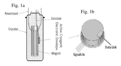
Active Cryogenic Electronic Envelope
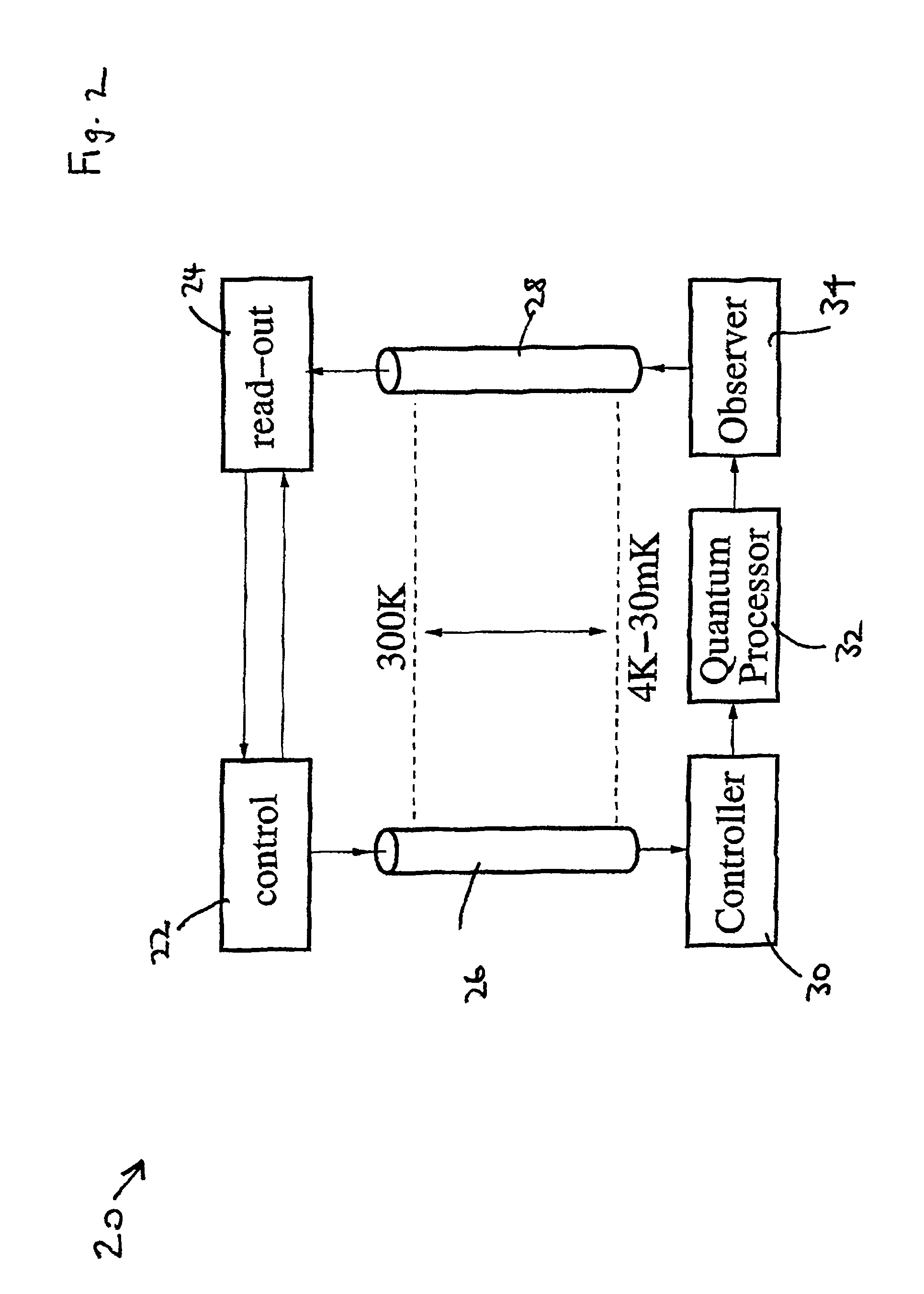
PatentActiveUS20160061538A1
Innovation
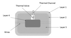
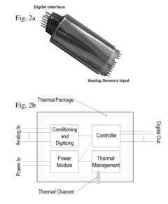
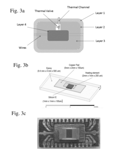
- A data acquisition module capable of operating at cryogenic temperatures, which resides inside a cryostat and maintains electronic components within a controlled thermal envelope, allowing conventional electronics to function effectively at temperatures as low as 0° K, thereby reducing thermal noise and simplifying the feedthrough interface.
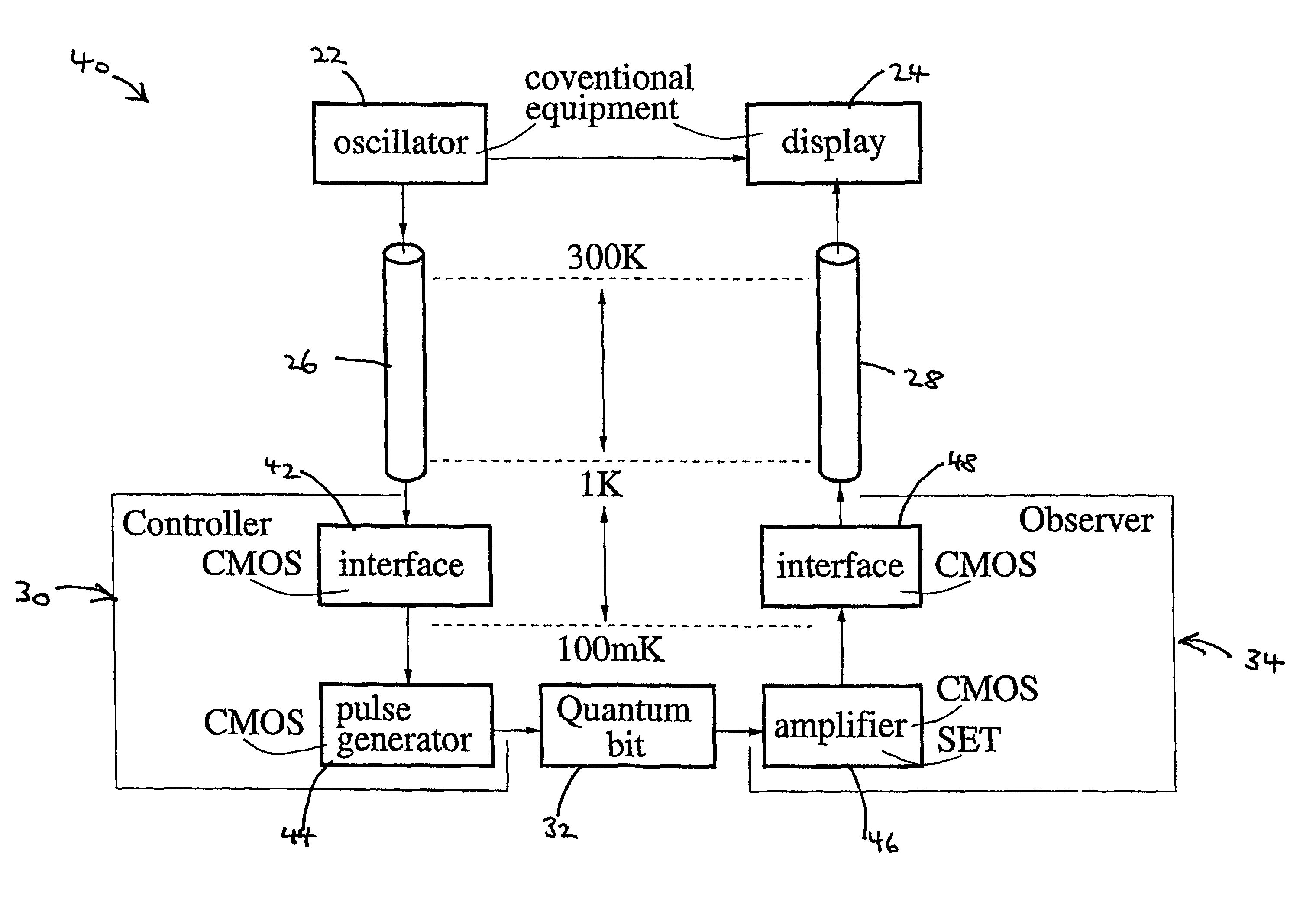
Interfacing at low temperature using CMOS technology
PatentActiveUS7911265B2
Innovation
- The development of ultra-thin silicon-on-insulator (SOI) CMOS technology for fabricating controller and observer circuits, which utilize SOI-CMOSFETs to achieve high unity-gain frequency, rapid pulse edge transition times, high bandwidth, and low power operation, enabling effective control and measurement of quantum bits at low temperatures.
Radiation Hardening Techniques for Cryogenic Environments
Radiation hardening techniques for cryogenic environments represent a critical frontier in space exploration technology, particularly as missions venture deeper into the solar system where extreme cold and intense radiation coexist. Traditional radiation hardening approaches developed for room-temperature electronics often prove inadequate when components operate at temperatures approaching absolute zero.
The fundamental challenge lies in the interaction between radiation effects and low-temperature physics. At cryogenic temperatures, charge carrier mobility changes significantly, affecting how semiconductor materials respond to radiation-induced displacement damage and ionization events. This necessitates specialized hardening techniques specifically designed for the cryogenic domain.
Material selection becomes paramount in cryogenic radiation hardening. Silicon-germanium (SiGe) heterojunction bipolar transistors have demonstrated remarkable radiation tolerance at temperatures as low as 4 Kelvin. Similarly, gallium nitride (GaN) and silicon carbide (SiC) wide-bandgap semiconductors exhibit enhanced performance in combined radiation and cryogenic environments due to their stronger atomic bonds and higher displacement energies.
Circuit-level hardening techniques have evolved to address the unique challenges of cryogenic radiation environments. Redundant circuit architectures implementing triple modular redundancy (TMR) with majority voting systems show improved effectiveness at low temperatures, as the reduced thermal noise enhances signal integrity in the voting mechanisms. Additionally, specialized layout techniques such as enclosed-gate transistors and guard rings demonstrate enhanced effectiveness at cryogenic temperatures.
Shielding methodologies for cryogenic electronics require careful consideration of thermal conductivity alongside radiation attenuation properties. Multi-layered shields incorporating high-Z materials (tungsten, tantalum) for gamma protection and hydrogen-rich compounds for neutron moderation must maintain thermal isolation characteristics critical for cryogenic operation.
Recent innovations include self-healing circuit designs that leverage the unique properties of certain materials at cryogenic temperatures to automatically recover from radiation damage. For instance, some superconducting materials demonstrate an ability to "anneal" radiation-induced defects when cycled through specific temperature ranges, effectively restoring their electrical properties.
Testing protocols for cryogenic radiation hardness assurance have advanced significantly, with specialized facilities now capable of simultaneous exposure to space-representative radiation spectra while maintaining components at temperatures below 20 Kelvin. These facilities enable more accurate qualification of components intended for missions to the outer planets, where radiation belts can be orders of magnitude more intense than Earth's Van Allen belts.
International Collaboration in Deep Space Cryogenic Research
The landscape of deep space cryogenic research has evolved into a highly collaborative international endeavor, with multiple space agencies, research institutions, and private companies forming strategic partnerships to overcome the immense challenges of developing cryogenic electronics for extreme environments. NASA, ESA, JAXA, and Roscosmos have established the International Cryogenic Technology Consortium (ICTC), which coordinates research efforts and facilitates knowledge sharing across borders. This consortium has been instrumental in standardizing testing protocols for cryogenic components, ensuring compatibility between systems developed by different nations.
The European Union's Horizon Europe program has allocated €120 million specifically for international collaboration in space cryogenic technologies, supporting joint ventures between European research institutions and partners from the United States, Japan, and Canada. These collaborations have yielded significant breakthroughs, including the development of superconducting quantum interference devices (SQUIDs) that maintain functionality at temperatures approaching absolute zero while withstanding radiation levels encountered in deep space.
China's space agency CNSA has recently opened its Advanced Cryogenics Laboratory to international researchers, marking a shift toward more open scientific exchange in this critical field. This facility houses state-of-the-art equipment for testing semiconductor behavior at temperatures below 10 Kelvin, providing valuable resources to the global research community. Similarly, India's ISRO has partnered with academic institutions across five continents to develop cryocooler technologies that can maintain stable ultra-low temperatures with minimal power consumption.
Private sector involvement has accelerated international collaboration, with companies like Blue Origin, SpaceX, and Airbus Defense and Space investing in shared research initiatives. The Cryogenic Electronics Global Innovation Hub, headquartered in Zurich with satellite facilities in Tokyo, Houston, and Singapore, represents a novel approach to public-private partnership, bringing together researchers from diverse backgrounds to work on common technological challenges.
Academic exchange programs have become increasingly important, with specialized fellowships supporting the movement of researchers between institutions working on cryogenic electronics. The International Cryogenic Engineering Conference, held biennially, has become the premier forum for sharing advances in the field, consistently attracting over 2,000 participants from more than 45 countries. These gatherings have been crucial for establishing informal networks that often lead to formal research collaborations.
Funding mechanisms have evolved to support these international efforts, with multi-national grant programs specifically designed to incentivize cross-border research teams. The Deep Space Cryogenics Initiative, jointly funded by 12 countries, provides competitive grants for collaborative projects addressing key technological barriers, particularly focusing on radiation-hardened superconducting circuits and long-duration cryocooler reliability.
Unlock deeper insights with PatSnap Eureka Quick Research — get a full tech report to explore trends and direct your research. Try now!
Generate Your Research Report Instantly with AI Agent
Supercharge your innovation with PatSnap Eureka AI Agent Platform!