

Cryogenic Electronics: Integrative Approaches in Semiconductor Design
SEP 29, 202510 MIN READ
Generate Your Research Report Instantly with AI Agent
Patsnap Eureka helps you evaluate technical feasibility & market potential.
Cryogenic Electronics Evolution and Research Objectives
Cryogenic electronics represents a frontier domain at the intersection of quantum physics and semiconductor engineering, with roots dating back to the 1950s when researchers first observed superconductivity phenomena at extremely low temperatures. The field has evolved from theoretical curiosity to practical application, driven by the increasing demands for high-performance computing systems with reduced power consumption and enhanced processing capabilities.
The evolution of cryogenic electronics has been marked by several significant milestones. Initial research focused primarily on understanding the fundamental behavior of materials at temperatures approaching absolute zero. By the 1980s, the development of Josephson junctions enabled the first practical applications in metrology and sensing. The 1990s witnessed the emergence of Rapid Single Flux Quantum (RSFQ) logic, offering switching speeds orders of magnitude faster than conventional semiconductor technologies while consuming significantly less power.
Recent advancements have been catalyzed by the growing interest in quantum computing, which requires precise control of quantum states at cryogenic temperatures. This has spurred innovation in cryogenic control electronics, interfacing technologies, and specialized semiconductor designs optimized for low-temperature operation. The convergence of superconducting circuits with traditional semiconductor technologies has opened new possibilities for hybrid systems that leverage the advantages of both domains.
The primary research objectives in cryogenic electronics currently focus on several key areas. First, developing semiconductor devices specifically engineered to function optimally at cryogenic temperatures, addressing challenges such as carrier freeze-out and altered mobility characteristics. Second, creating integrated circuit architectures that can operate reliably across extreme temperature gradients, from room temperature to below 4 Kelvin.
Another critical objective involves improving the energy efficiency of cryogenic systems, particularly reducing the thermal load generated by control electronics. This includes research into novel materials with favorable properties at low temperatures and innovative circuit designs that minimize heat dissipation. Additionally, there is significant interest in developing standardized interfaces between cryogenic and room-temperature electronics to facilitate broader adoption of these technologies.
The field is also pursuing advances in packaging and interconnect technologies capable of withstanding thermal cycling while maintaining signal integrity. This encompasses research into specialized materials, connection methods, and thermal management strategies tailored to the unique constraints of cryogenic environments.
Looking forward, the trajectory of cryogenic electronics research aims toward greater integration density, improved reliability, and enhanced performance metrics. The ultimate goal is to establish a comprehensive technological foundation that enables practical, scalable applications across quantum computing, space exploration, medical imaging, and next-generation telecommunications systems.
Market Analysis for Cryogenic Semiconductor Applications
The cryogenic semiconductor market is experiencing significant growth driven by quantum computing advancements and high-performance computing needs. Current market size estimates place the global cryogenic electronics sector at approximately $4.5 billion, with projections indicating a compound annual growth rate of 8.7% through 2028. This growth trajectory is primarily fueled by substantial investments from both private technology corporations and government research initiatives.
Quantum computing represents the largest application segment, accounting for nearly 45% of the cryogenic semiconductor market. Major technology companies including IBM, Google, and Intel have established dedicated quantum computing divisions with significant capital allocation toward cryogenic semiconductor development. The quantum computing market itself is projected to reach $1.7 billion by 2026, creating substantial demand for specialized cryogenic components.
Scientific research applications constitute the second-largest market segment at 25%, encompassing particle physics, astronomy, and materials science. The remaining market share is distributed across medical imaging (15%), aerospace and defense (10%), and emerging applications (5%) including superconducting data centers.
Geographically, North America dominates with approximately 42% market share, followed by Europe (28%), Asia-Pacific (22%), and other regions (8%). The United States maintains leadership through substantial DARPA and Department of Energy funding programs specifically targeting cryogenic computing technologies. However, China has recently accelerated investments in this sector, with government funding increasing by 35% annually since 2019.
Customer segmentation reveals three primary buyer categories: research institutions (40%), technology corporations (35%), and government/defense organizations (25%). Each segment demonstrates distinct purchasing behaviors and requirements, with research institutions prioritizing customization capabilities, while corporate buyers emphasize scalability and integration potential.
Key market drivers include the quantum computing race, increasing demand for energy-efficient computing solutions, and advancements in superconducting materials. The primary market restraints remain the high costs of cryogenic cooling infrastructure, technical complexity of integration with conventional electronics, and limited commercial-scale manufacturing capabilities.
The market demonstrates a classic technology adoption curve, currently transitioning from early adopters to early majority phase for certain applications. Industry analysts predict a potential inflection point within 3-5 years as manufacturing processes mature and integration challenges are addressed, potentially expanding the addressable market by 2-3 times its current size.
Global Cryogenic Electronics Development Status and Barriers
Cryogenic electronics represents a frontier technology domain that operates semiconductor devices at extremely low temperatures, typically below 120K. The global development landscape of this field exhibits significant regional disparities, with concentrated research efforts primarily in North America, Europe, and parts of Asia. The United States maintains leadership through substantial investments from both DARPA and private sector entities like IBM and Google, focusing particularly on quantum computing applications. European research clusters, notably in the Netherlands and Germany, have established strong foundations in superconducting electronics and quantum technologies.
The current technological barriers in cryogenic electronics are multifaceted and challenging. Device physics at ultra-low temperatures presents fundamental challenges as conventional semiconductor models become inadequate. Electron mobility, carrier concentration, and band structure all undergo significant alterations at cryogenic temperatures, necessitating new theoretical frameworks and simulation tools. Material compatibility issues emerge as thermal expansion coefficients diverge dramatically between different materials at cryogenic temperatures, creating mechanical stress that compromises device integrity.
Power dissipation management represents another critical barrier. While cryogenic operation reduces certain thermal effects, the cooling systems themselves have limited capacity, creating a stringent power budget for cryogenic circuits. This constraint is particularly problematic for complex systems requiring substantial computational resources. The integration challenges between room temperature and cryogenic components further complicate system design, as signal integrity must be maintained across extreme temperature gradients.
Manufacturing processes optimized for cryogenic operation remain underdeveloped. Standard semiconductor fabrication techniques require significant modification to produce devices that perform optimally at cryogenic temperatures. The lack of standardized design tools and process development kits (PDKs) specifically for cryogenic electronics impedes broader adoption and innovation in the field.
Testing infrastructure presents additional complications, as specialized equipment for characterizing devices at cryogenic temperatures is expensive and not widely available. This limitation creates bottlenecks in the development cycle and increases costs. The reliability and aging mechanisms of semiconductor devices at cryogenic temperatures remain poorly understood, with limited long-term operational data available to guide design decisions.
Despite these challenges, recent advances in superconducting materials, quantum computing requirements, and specialized cryogenic semiconductor processes are gradually addressing these barriers. International collaboration between academic institutions, government laboratories, and industry partners has accelerated in recent years, though significant gaps in standardization and manufacturing infrastructure persist across the global landscape.
Current Integrative Approaches in Cryogenic Semiconductor Design
01 Cryogenic semiconductor device design
Specialized semiconductor designs for operation at extremely low temperatures, focusing on materials and structures that maintain functionality in cryogenic environments. These designs address challenges such as carrier freeze-out and thermal contraction while optimizing performance characteristics like reduced leakage current and improved carrier mobility at low temperatures.- Cryogenic semiconductor device design: Semiconductor devices designed to operate at cryogenic temperatures require special considerations for material selection and circuit design. These devices leverage unique properties of semiconductors at extremely low temperatures to achieve enhanced performance characteristics such as reduced noise, increased carrier mobility, and improved energy efficiency. The designs often incorporate specialized insulation and thermal management techniques to maintain stable operation in cryogenic environments.
- Cooling systems for cryogenic electronics: Specialized cooling systems are essential for maintaining semiconductor devices at cryogenic temperatures. These systems may utilize liquid helium, liquid nitrogen, or mechanical cryocoolers to achieve and maintain the required low temperatures. Advanced designs incorporate efficient heat transfer mechanisms, thermal isolation techniques, and precise temperature control to ensure optimal performance of cryogenic electronic components while minimizing cooling power requirements.
- Superconducting circuit integration: Integration of superconducting materials and circuits with semiconductor devices enables novel functionalities at cryogenic temperatures. These hybrid systems combine the benefits of superconducting elements (zero resistance, quantum effects) with traditional semiconductor technology. Design considerations include interface engineering between superconducting and semiconductor materials, signal conversion between different operating regimes, and specialized fabrication techniques compatible with both technology platforms.
- Thermal management and isolation techniques: Effective thermal management is critical for cryogenic electronic systems to maintain stable operating temperatures while minimizing heat leakage. Designs incorporate specialized thermal isolation structures, multi-stage cooling arrangements, and careful material selection to manage thermal gradients. Advanced techniques include vacuum insulation, radiation shields, and strategic placement of components to optimize thermal performance while ensuring reliable electrical connections between temperature zones.
- Quantum computing hardware implementation: Cryogenic semiconductor designs for quantum computing applications focus on creating and controlling quantum bits (qubits) while managing the extreme cooling requirements. These designs address challenges such as qubit coherence time, control signal integrity at low temperatures, and integration of classical control electronics with quantum elements. Specialized interconnect technologies, low-power control circuits, and noise mitigation techniques are employed to create practical quantum processing hardware.
02 Cooling systems for electronic components
Advanced cooling technologies specifically designed for maintaining electronic components at cryogenic temperatures. These systems include specialized refrigeration cycles, thermal management solutions, and insulation techniques that enable stable operation of sensitive electronics in extreme cold environments while minimizing thermal gradients and power consumption.Expand Specific Solutions03 Superconducting circuit integration
Integration of superconducting materials and circuits with conventional semiconductor technology for cryogenic applications. These designs leverage the zero-resistance properties of superconductors at extremely low temperatures to create high-efficiency, low-power electronic systems with enhanced performance characteristics such as reduced noise and increased processing speed.Expand Specific Solutions04 Thermal isolation and packaging techniques
Specialized packaging and thermal isolation methods for cryogenic electronic systems that protect sensitive components from thermal stress while maintaining operational stability. These techniques include advanced materials for thermal barriers, vacuum insulation systems, and mechanical designs that accommodate differential thermal contraction between materials.Expand Specific Solutions05 Cryogenic testing and characterization methods
Specialized testing methodologies and equipment for evaluating semiconductor performance under cryogenic conditions. These approaches enable accurate characterization of electronic components at extremely low temperatures, including measurement of critical parameters such as threshold voltage shifts, leakage currents, and switching speeds to ensure reliable operation in cryogenic environments.Expand Specific Solutions
Leading Organizations in Cryogenic Electronics Research
Cryogenic Electronics is currently in a transitional phase from research to early commercialization, with an estimated market size of $2-3 billion and projected growth to $8-10 billion by 2030. The technology maturity varies across applications, with quantum computing implementations leading development. Key players demonstrate diverse approaches: IBM and Microsoft focus on quantum computing integration; SeeQC and Semiqon develop specialized quantum processors; while established semiconductor manufacturers like TSMC, GlobalFoundries, and SK hynix invest in cryogenic-compatible fabrication processes. Academic institutions including MIT and McGill University contribute fundamental research, while Applied Materials and Infineon Technologies develop enabling components. The competitive landscape shows strategic partnerships forming between research institutions and commercial entities to overcome significant technical challenges in scaling cryogenic electronic systems.
International Business Machines Corp.
Technical Solution: IBM has pioneered cryogenic electronics through their superconducting qubit technology and cryogenic control systems. Their approach integrates Josephson junction-based superconducting circuits operating at millikelvin temperatures with specialized cryogenic control electronics. IBM's Eagle quantum processor features 127 qubits with improved coherence times through advanced materials engineering and specialized fabrication techniques. Their cryogenic control architecture includes custom-designed cryogenic amplifiers, circulators, and multiplexed readout systems that minimize thermal load while maintaining signal integrity. IBM has also developed specialized CMOS circuits that can operate at 4K temperatures, bridging the gap between quantum processing elements and room-temperature control systems. Their roadmap includes developing increasingly integrated cryogenic control systems with higher qubit counts and reduced signal latency.
Strengths: Industry-leading expertise in superconducting qubit technology; extensive infrastructure for cryogenic testing; advanced materials engineering capabilities. Weaknesses: High power consumption for cooling systems; scalability challenges for control electronics; complexity in system integration requiring specialized expertise.
Microsoft Technology Licensing LLC
Technical Solution: Microsoft has developed a comprehensive approach to cryogenic electronics through their topological quantum computing initiative. Their technology centers on specialized semiconductor designs that support Majorana fermion-based qubits operating at ultra-low temperatures. Microsoft's cryogenic control architecture includes custom-designed CMOS circuits that function at temperatures below 100mK, with specialized interconnects designed to minimize thermal loading. Their approach emphasizes scalability through modular design, with each module containing localized control electronics to reduce signal path lengths and improve coherence times. Microsoft has pioneered materials innovations including specialized III-V semiconductor heterostructures optimized for low-temperature operation, and has developed proprietary fabrication techniques for creating topological superconductor interfaces. Their cryogenic electronics roadmap includes increasingly integrated control systems with reduced power dissipation and improved signal integrity, targeting systems with thousands of logical qubits.
Strengths: Substantial research investment in topological quantum approaches; strong systems integration expertise; advanced materials research capabilities. Weaknesses: Unproven topological qubit approach compared to more established technologies; high technical complexity; significant cooling requirements for large-scale systems.
Critical Patents and Innovations in Cryogenic Electronics
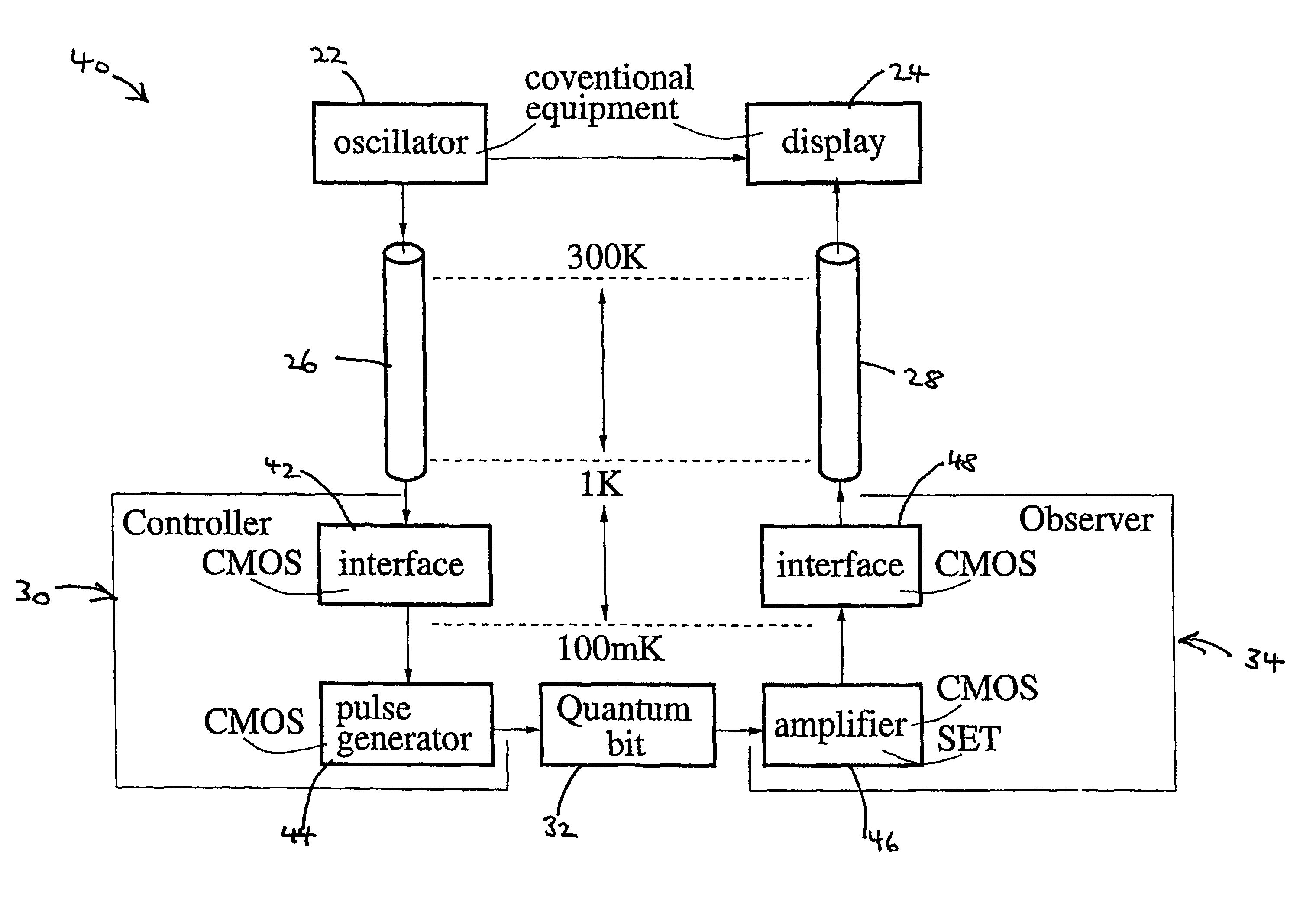
Interfacing at low temperature using CMOS technology
PatentActiveUS7911265B2
Innovation
- The development of ultra-thin silicon-on-insulator (SOI) CMOS technology for fabricating controller and observer circuits, which utilize SOI-CMOSFETs to achieve high unity-gain frequency, rapid pulse edge transition times, high bandwidth, and low power operation, enabling effective control and measurement of quantum bits at low temperatures.
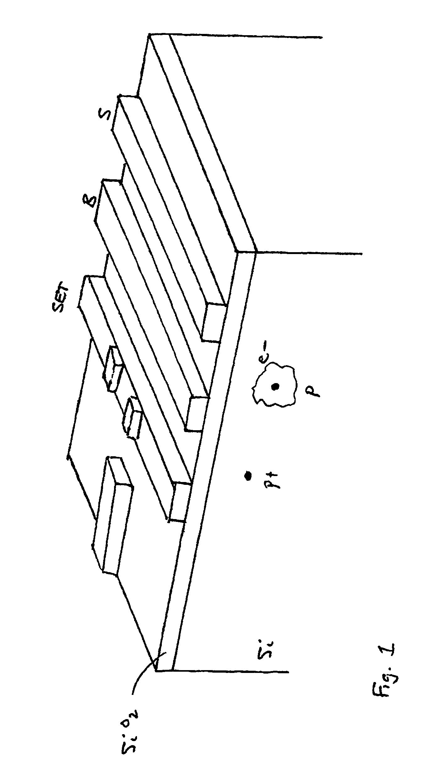
Electronic components employing field ionization
PatentWO2021086871A1
Innovation
- The use of field ionization techniques to reverse dopant freeze-out, enabling the operation of diodes and transistors at low temperatures with improved performance characteristics, including larger sub-threshold slopes and lower power consumption, by applying electric fields to ionize dopants and increase carrier concentrations.


Materials Science Advancements for Cryogenic Applications
The evolution of cryogenic electronics has been significantly propelled by breakthroughs in materials science. Traditional semiconductor materials exhibit altered electrical properties at extremely low temperatures, necessitating specialized materials engineered specifically for cryogenic environments. Recent advancements have focused on developing novel superconducting materials with higher critical temperatures, reducing the cooling requirements while maintaining quantum coherence.
Silicon-germanium (SiGe) heterojunction bipolar transistors have emerged as promising candidates for cryogenic applications due to their enhanced carrier mobility at low temperatures. Research indicates that SiGe-based circuits can operate efficiently at temperatures as low as 4K, making them suitable for integration with quantum computing systems. Additionally, III-V compound semiconductors like gallium arsenide (GaAs) and indium phosphide (InP) demonstrate superior electron mobility at cryogenic temperatures compared to silicon.
Superconducting materials research has yielded significant progress in niobium-based technologies. Niobium nitride (NbN) and niobium titanium nitride (NbTiN) thin films exhibit excellent superconducting properties at liquid helium temperatures, enabling the development of Josephson junction-based circuits with minimal energy dissipation. These materials form the foundation for superconducting quantum interference devices (SQUIDs) and rapid single flux quantum (RSFQ) logic circuits.
Thermal management materials represent another critical area of advancement. Novel thermal interface materials with enhanced thermal conductivity at cryogenic temperatures help address the challenges of heat dissipation in densely packed cryogenic circuits. Diamond-based substrates, with their exceptional thermal conductivity properties, are being explored as potential platforms for high-performance cryogenic electronics.
Dielectric materials for cryogenic applications have also seen significant improvements. Materials like silicon dioxide (SiO2) and silicon nitride (Si3N4) maintain their insulating properties at extremely low temperatures while minimizing parasitic capacitance effects. Research into amorphous dielectrics with reduced loss tangents at cryogenic temperatures has enabled the development of high-Q resonators essential for quantum information processing.
Packaging materials compatible with thermal cycling between room temperature and cryogenic conditions represent a persistent challenge. Recent developments in ceramic-based packaging solutions and specialized polymers with matched coefficients of thermal expansion have improved reliability during thermal cycling. These materials innovations enable more robust integration of cryogenic electronic components with room-temperature control systems.
The convergence of these materials science advancements is creating new possibilities for hybrid cryogenic-CMOS architectures, potentially bridging the gap between quantum processing units operating at millikelvin temperatures and conventional semiconductor control electronics.
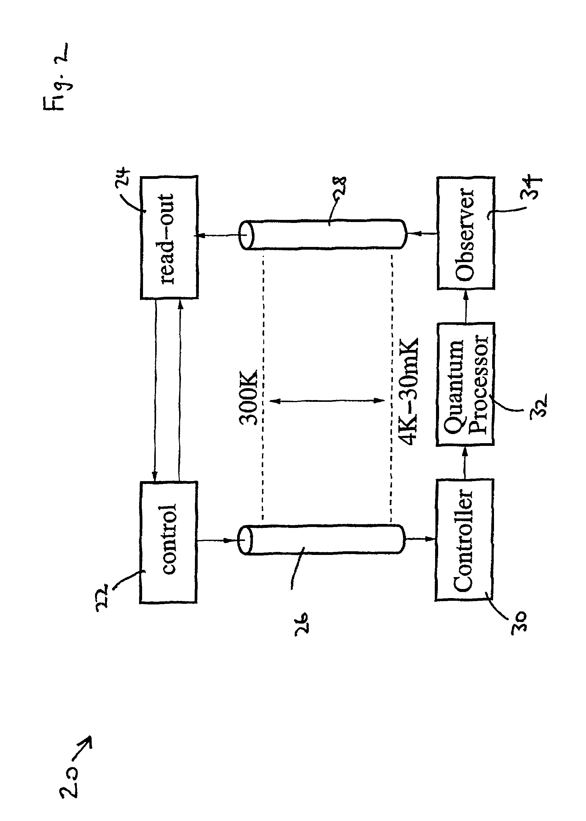
Quantum Computing Implications of Cryogenic Electronics
Cryogenic electronics represents a transformative technology for quantum computing, enabling unprecedented computational capabilities through the integration of superconducting materials and ultra-low temperature semiconductor designs. The quantum computing landscape is fundamentally dependent on cryogenic electronics, as quantum bits (qubits) require temperatures approaching absolute zero to maintain quantum coherence and minimize decoherence effects that would otherwise compromise computational integrity.
The integration of cryogenic electronics into quantum computing architectures addresses several critical challenges in quantum information processing. By operating at millikelvin temperatures, these specialized electronic components significantly reduce thermal noise, allowing for more precise qubit manipulation and readout. This temperature-dependent performance enhancement directly translates to improved quantum gate fidelities and extended coherence times, both essential metrics for practical quantum advantage.
Scalability of quantum systems represents another domain where cryogenic electronics delivers substantial benefits. As quantum processors increase in complexity from dozens to thousands of qubits, the conventional approach of routing control signals from room-temperature electronics becomes physically untenable due to thermal loading and wiring constraints. Cryogenic control electronics positioned in close proximity to the quantum processor can dramatically reduce these limitations, enabling the development of larger, more powerful quantum computing systems.
The material science advancements driving cryogenic electronics—particularly in superconducting circuits and specialized semiconductor designs—have parallel applications in quantum sensing and quantum communication. These adjacent quantum technologies benefit from the same ultra-low temperature operating environments, creating a technological ecosystem where innovations in cryogenic electronics yield benefits across multiple quantum domains.
Economic implications of this technological convergence are substantial. The global quantum computing market, projected to reach $65 billion by 2030, will increasingly rely on cryogenic electronic solutions. Companies developing expertise in this specialized field position themselves advantageously within the quantum supply chain, potentially capturing significant market share as quantum computing transitions from research laboratories to commercial applications.
Looking forward, the co-evolution of quantum computing architectures and cryogenic electronics will likely accelerate, with each field driving innovations in the other. Breakthroughs in materials science, circuit design, and fabrication techniques specifically optimized for cryogenic environments will directly enhance quantum computing capabilities, potentially accelerating the timeline toward practical quantum advantage in fields ranging from materials science to cryptography and pharmaceutical development.
Unlock deeper insights with Patsnap Eureka Quick Research — get a full tech report to explore trends and direct your research. Try now!
Generate Your Research Report Instantly with AI Agent
Supercharge your innovation with Patsnap Eureka AI Agent Platform!