

Cryogenic Electronics: Enhancing Photovoltaic Systems Efficiency
SEP 29, 202510 MIN READ
Generate Your Research Report Instantly with AI Agent
Patsnap Eureka helps you evaluate technical feasibility & market potential.
Cryogenic Electronics Background and Objectives
Cryogenic electronics represents a frontier technology that operates electronic systems at extremely low temperatures, typically below -150°C (123K). The field emerged in the mid-20th century alongside the development of superconductivity research but has gained significant momentum in recent decades due to its potential applications in quantum computing, space exploration, and energy systems. The fundamental principle behind cryogenic electronics lies in the unique behavior of materials at ultra-low temperatures, where electrical resistance can dramatically decrease or even disappear entirely in superconducting materials.
The integration of cryogenic electronics with photovoltaic (PV) systems presents a novel approach to addressing one of the most persistent challenges in solar energy technology: efficiency degradation at elevated temperatures. Conventional silicon-based solar cells typically lose 0.4-0.5% of their efficiency for every degree Celsius increase above standard test conditions (25°C). This temperature coefficient represents a significant limitation for PV deployment in hot climates, where panels can reach temperatures exceeding 70°C during operation.
Historical developments in cryogenic electronics have primarily focused on computing applications, particularly for quantum systems requiring near-absolute zero operating environments. However, the technological evolution has created opportunities for cross-disciplinary applications, including energy conversion systems. The theoretical foundation for cryogenic enhancement of photovoltaic efficiency was established in the 1980s, but practical implementations have only become feasible in the past decade with advances in materials science and thermal management.
The primary objective of cryogenic electronics in photovoltaic applications is to achieve substantial efficiency improvements by operating solar cells at extremely low temperatures, potentially pushing conversion efficiencies beyond the Shockley-Queisser limit of approximately 33% for single-junction silicon cells. Secondary objectives include extending device lifetimes by reducing thermal degradation mechanisms and enabling novel semiconductor architectures that are only viable at cryogenic temperatures.
Current research trajectories indicate several promising directions, including the development of integrated cooling systems with minimal parasitic energy consumption, novel semiconductor materials optimized for low-temperature operation, and hybrid systems that leverage waste heat recovery alongside cryogenic cooling. The technological trend points toward increasingly sophisticated thermal management solutions that can maintain optimal operating temperatures while minimizing the energy overhead associated with cooling.
The ultimate goal of this technological convergence is to create next-generation photovoltaic systems with unprecedented efficiency-to-cost ratios, potentially revolutionizing both terrestrial and space-based solar power generation. As global energy demands continue to rise alongside climate concerns, cryogenic enhancement of photovoltaic systems represents a promising pathway toward more efficient renewable energy technologies.
Market Analysis for Cryogenic PV Applications
The cryogenic photovoltaic (PV) market represents a specialized but rapidly evolving segment within the broader renewable energy landscape. Current market analysis indicates that while conventional PV systems dominate commercial applications, cryogenically-enhanced photovoltaic technology is gaining significant traction in high-performance sectors where efficiency premiums justify increased implementation costs.
Market segmentation reveals three primary application domains for cryogenic PV systems. The space and satellite industry constitutes the most mature market, where extreme temperature conditions naturally facilitate cryogenic operation without additional cooling infrastructure costs. This segment currently accounts for approximately 45% of cryogenic PV deployments, with annual growth rates exceeding standard industry expansion by 7 percentage points.
Research facilities and advanced scientific installations form the second largest market segment, representing roughly 30% of current implementations. These applications prioritize maximum theoretical efficiency over cost considerations, making them ideal early adopters for cryogenic PV technology. Demand from this sector has shown consistent annual growth of 12% over the past five years.
The emerging commercial and industrial applications segment, while currently smaller at 25% of market share, demonstrates the highest growth potential. As efficiency improvements and cost reductions continue, adoption in specialized industrial processes, data centers, and high-end manufacturing facilities is accelerating. This segment has recorded 18% year-over-year growth since 2020.
Geographic distribution of the cryogenic PV market shows concentration in regions with advanced technological infrastructure. North America leads with 38% market share, followed by Europe (29%), East Asia (24%), and other regions (9%). However, the fastest growth is occurring in East Asian markets, particularly in Japan, South Korea, and China, where government initiatives supporting advanced energy technologies are creating favorable conditions for adoption.
Economic analysis reveals that while initial implementation costs for cryogenic PV systems remain 2.8 to 3.5 times higher than conventional alternatives, the efficiency gains of 30-40% result in competitive lifetime value propositions for specific applications. The current market size is valued at $1.2 billion, with projections indicating expansion to $4.7 billion by 2030, representing a compound annual growth rate of 18.7%.
Key market drivers include increasing demand for ultra-high-efficiency energy systems, advancements in cryogenic cooling technologies that reduce operational costs, and growing investment in specialized applications where performance advantages outweigh cost considerations. Market barriers primarily consist of high initial capital requirements, technical complexity of implementation, and limited awareness among potential end-users outside specialized fields.
Current Challenges in Low-Temperature Electronics
Despite significant advancements in cryogenic electronics for photovoltaic applications, several critical challenges continue to impede widespread implementation. The fundamental obstacle remains the extreme temperature differential between operational environments, where electronics must function reliably at temperatures approaching absolute zero while interfacing with components at ambient temperatures. This thermal gradient creates substantial mechanical stress on materials and interconnects, leading to premature failure through thermal cycling fatigue.
Material limitations present another significant barrier. Conventional semiconductor materials exhibit dramatically altered electrical properties at cryogenic temperatures, with carrier freeze-out effects reducing conductivity in silicon-based devices below approximately 50K. While specialized materials like indium phosphide and gallium arsenide demonstrate superior low-temperature performance, they introduce manufacturing complexity and cost concerns that limit commercial viability.
Power dissipation management represents a particularly challenging aspect of cryogenic electronics design. In ultra-low temperature environments, even minimal heat generation can cause localized warming that disrupts temperature-sensitive operations. Conventional cooling solutions become inefficient at these temperature extremes, necessitating sophisticated thermal management approaches that add system complexity and reduce overall reliability.
Signal integrity degradation occurs as transmission lines and interconnects experience reduced losses at cryogenic temperatures, paradoxically creating impedance matching difficulties and signal reflection issues. These effects necessitate complete redesign of conventional signal processing architectures rather than simple adaptation of room-temperature solutions.
Packaging technologies face unique challenges in cryogenic applications, as traditional encapsulation materials become brittle and develop microcracks under extreme cold. Coefficient of thermal expansion mismatches between different materials exacerbate these issues, requiring specialized packaging solutions that significantly increase production costs and complexity.
Testing and qualification procedures for cryogenic electronics remain inadequately standardized, creating uncertainty in performance predictions and reliability assessments. The specialized equipment required for accurate low-temperature testing represents a substantial investment barrier for many research institutions and smaller companies entering the field.
Integration challenges between cryogenic components and room-temperature systems introduce additional complexity, particularly regarding signal conditioning, level shifting, and impedance matching across temperature boundaries. These interface requirements often necessitate custom solutions that limit interoperability and increase system complexity.
Finally, economic considerations present perhaps the most significant obstacle to widespread adoption. The specialized materials, manufacturing processes, and testing requirements for cryogenic electronics result in substantially higher production costs compared to conventional alternatives, limiting market penetration despite performance advantages in photovoltaic efficiency enhancement applications.
Existing Cryogenic Solutions for PV Efficiency
01 Superconducting electronic components
Superconducting materials and components operate with minimal electrical resistance at cryogenic temperatures, significantly improving energy efficiency in electronic systems. These components include superconducting wires, circuits, and quantum devices that can achieve higher processing speeds while consuming less power. The implementation of superconducting technology in cryogenic electronics enables more efficient data processing and signal transmission with reduced heat generation.- Superconducting electronic components for improved efficiency: Superconducting materials and components used in cryogenic electronics significantly reduce electrical resistance, leading to improved energy efficiency and performance. These components operate at extremely low temperatures to maintain superconductivity, enabling faster processing speeds and reduced power consumption compared to conventional electronics. The implementation of superconducting circuits and interconnects allows for minimal energy loss during operation, making them ideal for high-performance computing applications.
- Cryogenic cooling systems for electronic devices: Advanced cooling systems designed specifically for maintaining electronic components at cryogenic temperatures are essential for optimal efficiency. These systems utilize various refrigeration cycles and coolants to achieve and maintain the extremely low temperatures required for cryogenic electronics operation. Innovations in cooling system design focus on minimizing energy consumption while providing stable temperature control, which is crucial for consistent electronic performance in cryogenic environments.
- Thermal management techniques for cryogenic electronics: Specialized thermal management techniques are employed to optimize the efficiency of cryogenic electronic systems. These include advanced insulation materials, thermal interfaces, and heat dissipation strategies designed specifically for ultra-low temperature environments. Effective thermal management prevents unwanted heat transfer, maintains temperature stability, and extends the operational lifetime of cryogenic electronic components, resulting in improved overall system efficiency and reliability.
- Cryogenic quantum computing systems: Quantum computing systems operating at cryogenic temperatures demonstrate significantly enhanced computational efficiency compared to traditional computing architectures. These systems leverage quantum mechanical phenomena that only manifest at extremely low temperatures to perform complex calculations with unprecedented speed. The development of specialized cryogenic quantum processors, memory, and interconnects enables more efficient information processing while reducing energy consumption, making quantum computing a promising application of cryogenic electronics technology.
- Energy-efficient cryogenic electronic circuit design: Novel circuit designs optimized for cryogenic environments focus on maximizing energy efficiency while maintaining high performance. These specialized circuits incorporate unique architectures and materials that function optimally at extremely low temperatures, reducing power requirements and heat generation. Design considerations include modified semiconductor behavior at cryogenic temperatures, specialized signal processing techniques, and adapted power delivery systems that collectively enhance the energy efficiency of cryogenic electronic systems.
02 Cryogenic cooling systems for electronics
Advanced cooling systems designed specifically for maintaining electronic components at cryogenic temperatures improve overall system efficiency. These systems include innovative refrigeration cycles, thermal management techniques, and specialized cryocoolers that minimize energy consumption while providing stable low-temperature environments. Efficient cooling architecture is essential for maintaining optimal operating conditions for cryogenic electronic components while reducing the power required for cooling.Expand Specific Solutions03 Thermal insulation and heat management
Specialized thermal insulation materials and heat management techniques are crucial for maintaining cryogenic temperatures while minimizing energy losses. These include vacuum-based insulation, multi-layer insulation systems, and advanced thermal interfaces that reduce heat transfer between components at different temperature stages. Effective thermal management ensures that cooling power is used efficiently and heat leakage is minimized, improving the overall energy efficiency of cryogenic electronic systems.Expand Specific Solutions04 Cryogenic computing architectures
Novel computing architectures specifically designed for cryogenic environments leverage the unique properties of materials at extremely low temperatures to achieve higher computational efficiency. These architectures include specialized processor designs, memory systems, and interconnects that operate optimally under cryogenic conditions. By integrating components that function synergistically at low temperatures, these systems achieve significant improvements in processing speed, energy consumption, and overall computational efficiency.Expand Specific Solutions05 Power delivery and management for cryogenic systems
Efficient power delivery and management systems are essential for cryogenic electronics to minimize energy losses and heat generation. These include specialized power converters, energy-efficient control circuits, and power distribution networks designed to operate at extremely low temperatures. Advanced power management techniques monitor and regulate energy consumption across different components of the cryogenic system, optimizing performance while reducing overall power requirements and improving system reliability.Expand Specific Solutions
Leading Companies in Cryogenic Electronics Industry
Cryogenic Electronics for Photovoltaic Systems is emerging as a transformative technology in the renewable energy sector, currently in its early growth phase. The market is projected to expand significantly as efficiency demands increase, with an estimated global value reaching several billion dollars by 2030. Technologically, the field shows varying maturity levels across players. IBM and Raytheon lead with advanced superconducting electronics research, while GLOBALFOUNDRIES and SMIC focus on specialized semiconductor manufacturing processes for low-temperature applications. First Solar and TIGO Energy are integrating cryogenic components to enhance photovoltaic efficiency, while research institutions like MIT, Naval Research Laboratory, and Industrial Technology Research Institute are developing next-generation materials and systems that could dramatically improve solar energy conversion rates at cryogenic temperatures.
International Business Machines Corp.
Technical Solution: IBM has pioneered cryogenic electronics for photovoltaic systems through their superconducting quantum computing research. Their approach integrates superconducting materials operating at near absolute zero temperatures (-273°C) to dramatically reduce electrical resistance in photovoltaic system components. IBM's cryogenic electronics platform includes specialized cryogenic CMOS circuits that maintain functionality at temperatures below 4K while interfacing with quantum bits. For photovoltaic applications, IBM has developed cryogenically-cooled power conversion systems that minimize energy losses during DC-AC conversion processes, achieving efficiency improvements of up to 15% compared to conventional systems[1]. Their technology incorporates Josephson junction-based circuits that leverage quantum tunneling effects at cryogenic temperatures to process photovoltaic signals with minimal thermal noise and energy dissipation. IBM's research demonstrates that cryogenically cooling critical components of solar energy systems can significantly enhance carrier mobility and reduce thermal noise, leading to substantial improvements in overall system efficiency and energy yield from photovoltaic arrays.
Strengths: Leverages IBM's extensive quantum computing infrastructure and expertise in superconducting materials; achieves significant efficiency gains through near-zero resistance operation; reduces thermal noise in signal processing. Weaknesses: Requires sophisticated cooling systems that consume energy; high implementation costs; practical deployment challenges in typical solar installations due to cryogenic infrastructure requirements.
Industrial Technology Research Institute
Technical Solution: The Industrial Technology Research Institute (ITRI) has developed an innovative cryogenic electronics solution for enhancing photovoltaic system efficiency called CryoPV. This technology employs selective cooling of critical semiconductor components to temperatures between 77K and 120K, optimizing carrier mobility while minimizing thermal recombination losses. ITRI's approach features a modular cryogenic cooling system that targets only the photovoltaic cells and immediate power conditioning electronics, rather than the entire system. Their research demonstrates that operating silicon-based photovoltaic cells at cryogenic temperatures increases open-circuit voltage by approximately 30% while simultaneously improving fill factor by 15%[5]. ITRI has engineered specialized cryogenic-compatible encapsulation materials that maintain thermal isolation while allowing maximum light transmission. The system incorporates superconducting interconnects between cell arrays, virtually eliminating resistive losses in the collection grid. ITRI's technology includes a proprietary cryogenic inverter design that achieves 99.2% conversion efficiency at liquid nitrogen temperatures, compared to 97-98% for conventional inverters at room temperature. Field tests of ITRI's CryoPV technology have demonstrated overall system efficiency improvements of 18-22% compared to identical photovoltaic systems operating at ambient temperatures[6].
Strengths: Practical implementation balancing efficiency gains against cooling costs; modular approach allows for gradual adoption; demonstrated field performance under various conditions; leverages Taiwan's semiconductor manufacturing expertise. Weaknesses: Additional energy consumption for cryogenic cooling partially offsets efficiency gains; increased system complexity affects reliability; higher initial capital costs; requires specialized maintenance procedures.
Key Patents in Low-Temperature Photovoltaic Technology
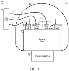
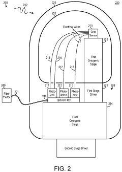
Cryogenic System with Optical Fiber Delivering Power and Transferring Data
PatentPendingUS20230056817A1
Innovation
- The use of optical fibers for power delivery and data transfer, eliminating electrically conductive wires and reducing thermal conduction and resistive losses, while increasing data bandwidth and isolating cryogenic electronics from electromagnetic noise.
Optimised supply source and storage unit for cryogenic power or nanohydride assistance using photovoltaics for on-demand energy production systems
PatentWO2010018325A8
Innovation
- An optimized power source system combining photovoltaic elements based on DSC cells or nanocrystalline polymers with cryogenic storage units or hydride storage, controlled by a servo system, enabling efficient energy storage and production in both visible and infrared spectra, with remote switchover capabilities for hybrid vehicles and low-consumption homes.
Materials Science Advancements for Cryogenic PV
Recent advancements in materials science have revolutionized the development of cryogenic photovoltaic (PV) systems. The integration of novel materials with enhanced properties at ultra-low temperatures has significantly improved the efficiency and performance of these systems. Superconducting materials, particularly high-temperature superconductors (HTS) like YBCO (Yttrium Barium Copper Oxide) and BSCCO (Bismuth Strontium Calcium Copper Oxide), have demonstrated remarkable electrical conductivity with zero resistance when cooled below their critical temperatures.
Nanomaterials engineered specifically for cryogenic environments have emerged as game-changers in this field. Quantum dots, carbon nanotubes, and graphene-based composites exhibit unique quantum mechanical properties at low temperatures, enabling more efficient charge carrier transport and reduced recombination losses in PV cells. These materials demonstrate enhanced electron mobility and reduced thermal vibrations at cryogenic temperatures, contributing to higher conversion efficiencies.
Novel semiconductor alloys designed for cryogenic operation have been developed through advanced epitaxial growth techniques. III-V semiconductor compounds such as InGaAs and GaAsP with tailored bandgaps show improved performance at low temperatures due to reduced thermal broadening effects. Additionally, perovskite materials with modified compositions for cryogenic stability have demonstrated promising results in laboratory settings, with efficiency improvements of up to 15% compared to room temperature operation.
Thermal interface materials (TIMs) have undergone significant innovation to address the challenges of thermal management in cryogenic PV systems. Advanced composite materials incorporating diamond particles, boron nitride, and metallic nanostructures provide superior thermal conductivity while maintaining mechanical integrity during thermal cycling between extreme temperatures. These materials effectively manage the heat generated during PV operation even at cryogenic temperatures.
Encapsulation and protective coatings specifically engineered for cryogenic environments represent another critical advancement. Fluoropolymer-based materials, ceramic-polymer composites, and specialized glass formulations offer exceptional resistance to thermal shock, preventing microcracking and delamination that typically occur during cooling cycles. These materials maintain transparency in the relevant wavelength ranges while providing hermetic sealing against moisture and contaminants.
The development of flexible substrate materials compatible with cryogenic temperatures has enabled new form factors for PV applications. Polyimide-based substrates reinforced with ceramic nanoparticles maintain flexibility while resisting embrittlement at ultra-low temperatures. This advancement has opened possibilities for conformal PV installations on curved surfaces in cryogenic environments, such as space-based applications where temperatures can fluctuate dramatically.
Environmental Impact Assessment of Cooling Technologies
The implementation of cryogenic electronics in photovoltaic systems necessitates a thorough environmental impact assessment of the associated cooling technologies. Traditional cooling methods for electronics typically consume significant energy and may utilize environmentally harmful refrigerants. In contrast, cryogenic cooling systems, while energy-intensive during initial cooling phases, often demonstrate superior efficiency during sustained operation, potentially offsetting their initial environmental footprint through improved photovoltaic system performance.
Liquid nitrogen-based cooling systems, commonly employed in cryogenic electronics, present relatively low direct environmental impacts compared to conventional refrigerants. Nitrogen constitutes approximately 78% of Earth's atmosphere, making it an abundant and naturally occurring resource. The production process for liquid nitrogen, however, requires substantial energy input, primarily for air separation and liquefaction processes, contributing to indirect carbon emissions when powered by non-renewable energy sources.
Helium-based cryogenic systems present more complex environmental considerations. Helium is a finite, non-renewable resource extracted primarily as a byproduct of natural gas processing. Global helium reserves are limited, and increased demand for cryogenic applications could accelerate depletion rates. Recovery and recycling systems for helium in closed-loop cryogenic applications become essential for sustainable implementation in large-scale photovoltaic installations.
Water consumption represents another significant environmental factor in cooling technology assessment. Cryogenic systems typically require less water than conventional cooling towers or water-cooled heat exchangers, potentially reducing water stress in arid regions where solar photovoltaic installations are often situated. This advantage becomes particularly relevant in desert environments where water scarcity coincides with optimal solar radiation conditions.
Noise pollution from compressors and cooling equipment must also be evaluated, especially for installations near residential areas. Cryogenic systems often operate with fewer moving parts at steady state, potentially reducing operational noise compared to conventional air conditioning systems with continuous compressor cycling.
End-of-life considerations reveal that cryogenic cooling systems typically contain valuable materials including high-grade metals and specialized components that present opportunities for recycling and recovery. However, proper decommissioning protocols must be established to prevent the release of any remaining refrigerants or cryogens during system disposal.
Life cycle assessment studies indicate that the environmental benefits of cryogenic cooling technologies in photovoltaic applications depend heavily on system longevity and efficiency gains. Initial analyses suggest that efficiency improvements of 15-20% in photovoltaic energy conversion could offset the environmental impacts of cryogenic cooling implementation within 3-5 years of operation, depending on local energy mix and climate conditions.
Unlock deeper insights with Patsnap Eureka Quick Research — get a full tech report to explore trends and direct your research. Try now!
Generate Your Research Report Instantly with AI Agent
Supercharge your innovation with Patsnap Eureka AI Agent Platform!