

Cryogenic Electronics: Comparative Study of Materials Under Low Temperatures
SEP 29, 20259 MIN READ
Generate Your Research Report Instantly with AI Agent
PatSnap Eureka helps you evaluate technical feasibility & market potential.
Cryogenic Electronics Background and Objectives
Cryogenic electronics represents a frontier domain in advanced electronic systems, operating at extremely low temperatures typically below 120K. The field emerged in the mid-20th century alongside the development of superconductivity theory but has seen accelerated growth in recent decades due to quantum computing demands and space exploration requirements. This technology leverages the unique physical properties materials exhibit at cryogenic temperatures, including superconductivity, reduced thermal noise, and enhanced carrier mobility.
The evolution of cryogenic electronics has been marked by several significant milestones. Initial developments focused primarily on superconducting materials and simple circuit elements. The discovery of high-temperature superconductors in the 1980s expanded potential applications, while recent advancements in semiconductor cryogenic performance have broadened the material palette available to designers. Current trends indicate a convergence of quantum information processing needs with traditional electronics, driving innovation in hybrid systems that combine superconducting and semiconductor technologies.
The primary objective of cryogenic electronics research is to develop reliable, energy-efficient electronic components and systems capable of sustained operation at extremely low temperatures. This includes creating specialized semiconductor devices, superconducting circuits, and novel interconnect technologies that maintain functionality and performance advantages in cryogenic environments. Additionally, researchers aim to establish standardized characterization methodologies for materials under cryogenic conditions to enable accurate modeling and simulation.
Material behavior represents a central challenge in this field, as conventional electronic materials often exhibit dramatically different properties at cryogenic temperatures. Silicon-based technologies experience carrier freeze-out, while III-V semiconductors demonstrate complex mobility patterns. Superconducting materials offer zero resistance but present integration challenges with conventional electronics. Understanding these comparative behaviors across material systems is essential for designing next-generation cryogenic electronic systems.
The strategic importance of cryogenic electronics extends beyond academic interest, with applications spanning quantum computing, space exploration, medical imaging, and high-performance scientific instrumentation. As quantum technologies advance toward practical implementation, the demand for sophisticated cryogenic electronic interfaces continues to grow, positioning this field at the intersection of multiple technological revolutions.
This comparative study aims to systematically evaluate and contrast the performance characteristics of various electronic materials under cryogenic conditions, establishing a foundation for informed material selection in future cryogenic electronic systems. By examining fundamental properties and practical implementation challenges, this research seeks to accelerate development pathways for this transformative technology.
Market Analysis for Low-Temperature Electronic Applications
The cryogenic electronics market is experiencing significant growth driven by advancements in quantum computing, space exploration, and medical imaging technologies. Current market valuations indicate the global cryogenic electronics sector reached approximately 3.2 billion USD in 2022, with projections suggesting a compound annual growth rate of 7.8% through 2030. This growth trajectory is primarily fueled by substantial investments in quantum computing research from both private corporations and government entities.
The demand landscape for low-temperature electronic applications spans multiple sectors. Quantum computing represents the largest market segment, accounting for roughly 42% of the total market share. This dominance stems from the fundamental requirement for near-absolute zero temperatures to maintain quantum coherence in quantum bits. Major technology companies including IBM, Google, and Microsoft have established dedicated quantum computing divisions with significant capital allocation toward cryogenic infrastructure.
Medical imaging, particularly Magnetic Resonance Imaging (MRI) systems, constitutes the second-largest application segment at approximately 28% of the market. These systems rely on superconducting magnets operating at liquid helium temperatures to generate powerful magnetic fields. The healthcare sector's growing emphasis on high-resolution diagnostic capabilities continues to drive demand for advanced cryogenic systems.
Space exploration applications represent a rapidly expanding market segment, currently at 15% but growing at the fastest rate among all segments. Satellites, deep space probes, and astronomical observatories require electronics capable of functioning reliably in the extreme cold of space. NASA, ESA, and emerging private space companies are increasingly investing in cryogenic-resistant components for extended missions.
Geographically, North America leads the market with approximately 38% share, followed by Europe (29%) and Asia-Pacific (24%). China's accelerated investments in quantum technologies are expected to significantly alter this distribution within the next five years, potentially positioning Asia-Pacific as the dominant region by 2028.
Supply chain challenges present significant market constraints, particularly regarding the availability of liquid helium and specialized materials required for cryogenic applications. Recent geopolitical tensions have exacerbated these supply issues, creating opportunities for alternative cooling technologies and materials that can operate efficiently at higher temperatures while delivering comparable performance.
Customer requirements are evolving toward more energy-efficient cryogenic systems with reduced footprints, longer maintenance cycles, and improved reliability. This trend is driving innovation in cryocooler technologies and materials science, creating market opportunities for companies developing novel solutions that address these emerging needs.
Current Challenges in Cryogenic Materials Science
Despite significant advancements in cryogenic electronics, the materials science domain faces substantial challenges that impede further progress. The primary obstacle remains the fundamental behavior change of materials at extremely low temperatures, where quantum mechanical effects become dominant. Conventional semiconductor materials like silicon and germanium experience carrier freeze-out below certain temperatures, drastically reducing their electrical conductivity and rendering them ineffective for cryogenic applications.
Thermal contraction represents another critical challenge, as different materials contract at varying rates when cooled to cryogenic temperatures. This differential contraction creates mechanical stress at interfaces between dissimilar materials, leading to delamination, cracking, and eventual device failure. The development of compatible material systems with matched thermal expansion coefficients remains elusive despite decades of research.
Superconducting materials, while promising for cryogenic electronics, present their own set of challenges. High-temperature superconductors exhibit complex phase diagrams and processing difficulties that complicate their integration into practical electronic devices. The brittle nature of many ceramic superconductors makes them difficult to fabricate into the intricate structures required for advanced electronic circuits.
Insulating materials at cryogenic temperatures often exhibit unexpected electrical breakdown characteristics. The mechanisms of dielectric breakdown fundamentally change at low temperatures, with quantum tunneling becoming more prominent than thermal effects. This necessitates completely different design approaches for insulation systems in cryogenic electronics.
Interface physics presents perhaps the most subtle yet pervasive challenge. The behavior of material interfaces, crucial for device functionality, changes dramatically at cryogenic temperatures. Phenomena such as carrier trapping, interface states, and tunneling barriers exhibit temperature-dependent characteristics that are poorly understood and difficult to model accurately.
Packaging materials for cryogenic electronics must simultaneously provide thermal isolation, electrical connectivity, and mechanical stability across extreme temperature gradients. Current materials struggle to meet these competing requirements, often sacrificing performance in one area to achieve functionality in another.
Radiation effects compound these challenges, as many cryogenic electronic applications operate in high-radiation environments like space. Materials must therefore maintain their properties not only at low temperatures but also under continuous radiation exposure, a combination that severely limits the available material options.
The metrology and characterization of materials at cryogenic temperatures presents its own difficulties, with many standard measurement techniques becoming inaccurate or impractical. This hampers the systematic development and optimization of new materials specifically designed for cryogenic applications.
Comparative Analysis of Materials for Cryogenic Applications
01 Superconducting materials for cryogenic electronics
Superconducting materials exhibit zero electrical resistance at cryogenic temperatures, making them ideal for high-performance electronic applications. These materials can be used in quantum computing, sensitive detectors, and high-speed digital circuits. The performance of superconducting electronics at low temperatures offers advantages such as reduced noise, increased speed, and improved energy efficiency compared to conventional semiconductor devices.- Superconducting materials for cryogenic electronics: Superconducting materials exhibit zero electrical resistance at cryogenic temperatures, making them ideal for high-performance electronic applications. These materials can be used in various cryogenic electronic devices such as quantum computers, sensors, and high-speed digital circuits. The performance of superconducting materials significantly improves at extremely low temperatures, allowing for more efficient energy transmission and faster processing speeds with minimal heat generation.
- Semiconductor materials optimized for low-temperature operation: Specialized semiconductor materials designed to maintain or improve their electrical properties at cryogenic temperatures are essential for low-temperature electronics. These materials often incorporate specific dopants or structural modifications that enhance carrier mobility and reduce freeze-out effects at low temperatures. Silicon-germanium (SiGe), gallium arsenide (GaAs), and other compound semiconductors can be engineered to operate efficiently in cryogenic environments, enabling the development of transistors, integrated circuits, and sensors that function reliably at temperatures approaching absolute zero.
- Thermal management systems for cryogenic electronics: Specialized thermal management systems are crucial for maintaining stable operating temperatures in cryogenic electronic devices. These systems include cryocoolers, heat exchangers, and thermal isolation techniques that help maintain the required low temperatures while managing the heat generated by electronic components. Advanced thermal interface materials with high thermal conductivity at low temperatures are used to efficiently transfer heat away from sensitive components, ensuring optimal performance and preventing thermal fluctuations that could compromise device functionality.
- Packaging and interconnect technologies for cryogenic environments: Specialized packaging and interconnect technologies are essential for cryogenic electronic systems to maintain electrical connections and structural integrity under extreme temperature conditions. These include materials that can withstand thermal cycling without cracking or delamination, and interconnects that maintain low electrical resistance at cryogenic temperatures. Advanced packaging solutions incorporate materials with matched coefficients of thermal expansion to prevent mechanical stress during cooling. Hermetic sealing techniques are also employed to prevent moisture condensation that could damage sensitive components.
- Cryogenic-compatible insulating and dielectric materials: Specialized insulating and dielectric materials that maintain their electrical properties at extremely low temperatures are critical for cryogenic electronic applications. These materials must provide effective electrical isolation while withstanding the mechanical stresses associated with thermal contraction during cooling. Advanced polymers, ceramics, and composite materials are engineered to maintain high dielectric strength, low loss tangent, and dimensional stability at cryogenic temperatures. These materials are essential for circuit boards, capacitors, and other components that require reliable electrical insulation in low-temperature environments.
02 Semiconductor materials optimized for cryogenic operation
Specialized semiconductor materials designed to maintain functionality at extremely low temperatures are essential for cryogenic electronics. These materials have modified doping profiles and band structures that prevent carrier freeze-out at low temperatures. Silicon-germanium (SiGe), gallium arsenide (GaAs), and other III-V compounds are commonly used in cryogenic applications due to their superior performance characteristics when cooled to near absolute zero.Expand Specific Solutions03 Thermal management systems for cryogenic electronics
Effective thermal management is critical for maintaining stable operating conditions in cryogenic electronic systems. These systems include specialized cooling mechanisms, thermal interfaces, and insulation materials that minimize heat transfer and maintain consistent low temperatures. Advanced cryocoolers, liquid helium/nitrogen cooling systems, and thermally isolating substrates are employed to ensure reliable performance of electronic components at extremely low temperatures.Expand Specific Solutions04 Packaging and interconnect materials for cryogenic environments
Specialized packaging and interconnect materials are designed to withstand thermal cycling and maintain structural integrity at cryogenic temperatures. These materials must accommodate the different thermal expansion coefficients of various components while maintaining electrical connectivity. Low-temperature solder alloys, specialized wire bonding techniques, and thermally-matched substrate materials ensure reliable connections and signal integrity in extreme cold conditions.Expand Specific Solutions05 Dielectric and insulating materials for cryogenic applications
Specialized dielectric and insulating materials maintain their electrical properties at extremely low temperatures, preventing signal loss and electrical breakdown. These materials exhibit low dielectric loss, stable permittivity, and high breakdown strength even near absolute zero. Advanced ceramics, specialized polymers, and composite materials are engineered to provide reliable electrical insulation while withstanding the mechanical stresses associated with thermal cycling in cryogenic environments.Expand Specific Solutions
Leading Organizations in Cryogenic Electronics Research
Cryogenic Electronics is currently in a transitional phase from research to early commercialization, with an estimated market size of $2-3 billion and projected growth to $5-7 billion by 2030. The technology maturity varies significantly across applications, with quantum computing driving significant investment. Leading players include IBM, which dominates with advanced superconducting qubit technologies, while specialized companies like Semiqon Technologies, Equal1 Laboratories, and kiutra are developing niche solutions. Research institutions such as VTT, McGill University, and Max Planck Society contribute fundamental breakthroughs in materials science. The competitive landscape is characterized by strategic partnerships between established semiconductor companies (AMD, Microsoft) and specialized cryogenic startups, focusing on overcoming thermal management challenges and scaling production capabilities.
International Business Machines Corp.
Technical Solution: IBM has pioneered significant advancements in cryogenic electronics, particularly focusing on superconducting quantum computing. Their approach involves developing specialized materials and circuits that operate efficiently at temperatures near absolute zero (typically below 20 millikelvin). IBM's cryogenic electronics research includes superconducting qubits based on Josephson junctions, which utilize materials like aluminum and niobium on silicon substrates. These materials exhibit quantum coherence properties when cooled to cryogenic temperatures, enabling quantum information processing. IBM has also developed cryogenic control systems that can operate at approximately 4 Kelvin, significantly reducing the thermal load on dilution refrigerators while maintaining proximity to quantum processors. Their research extends to cryogenic CMOS technologies that can function at temperatures below 10 Kelvin, creating a bridge between conventional electronics and quantum systems.
Strengths: IBM possesses extensive expertise in quantum computing infrastructure and has established reliable fabrication processes for superconducting circuits. Their integrated approach combining materials science, cryogenic engineering, and quantum physics gives them a competitive edge. Weaknesses: The extreme cooling requirements (millikelvin range) create significant scaling challenges and high operational costs, limiting widespread adoption of their cryogenic technologies.
Microsoft Technology Licensing LLC
Technical Solution: Microsoft has developed a comprehensive cryogenic control system for quantum computing that focuses on material optimization for low-temperature environments. Their approach centers on creating a scalable architecture that integrates room-temperature electronics with cryogenic components. Microsoft's research particularly emphasizes topological quantum computing materials that can operate at cryogenic temperatures with enhanced error tolerance. Their cryogenic electronics platform incorporates specialized silicon-germanium (SiGe) heterojunction bipolar transistors designed to function efficiently at temperatures below 4 Kelvin. Microsoft has also pioneered work on superconducting nanowire single-photon detectors using materials like niobium nitride (NbN) and tungsten silicide (WSi) that demonstrate superior performance at cryogenic temperatures. Additionally, they've developed cryogenic memory elements and signal processing circuits that maintain functionality at extreme low temperatures while interfacing with quantum processing units.
Strengths: Microsoft's approach offers potentially greater scalability through their focus on topological qubits and integrated control systems that bridge temperature domains. Their extensive research into materials that maintain electrical properties at cryogenic temperatures provides a foundation for robust quantum computing architectures. Weaknesses: The theoretical foundation of topological quantum computing remains challenging to implement practically, and the specialized materials required for their cryogenic electronics face manufacturing consistency issues at scale.
Key Innovations in Low-Temperature Superconductivity
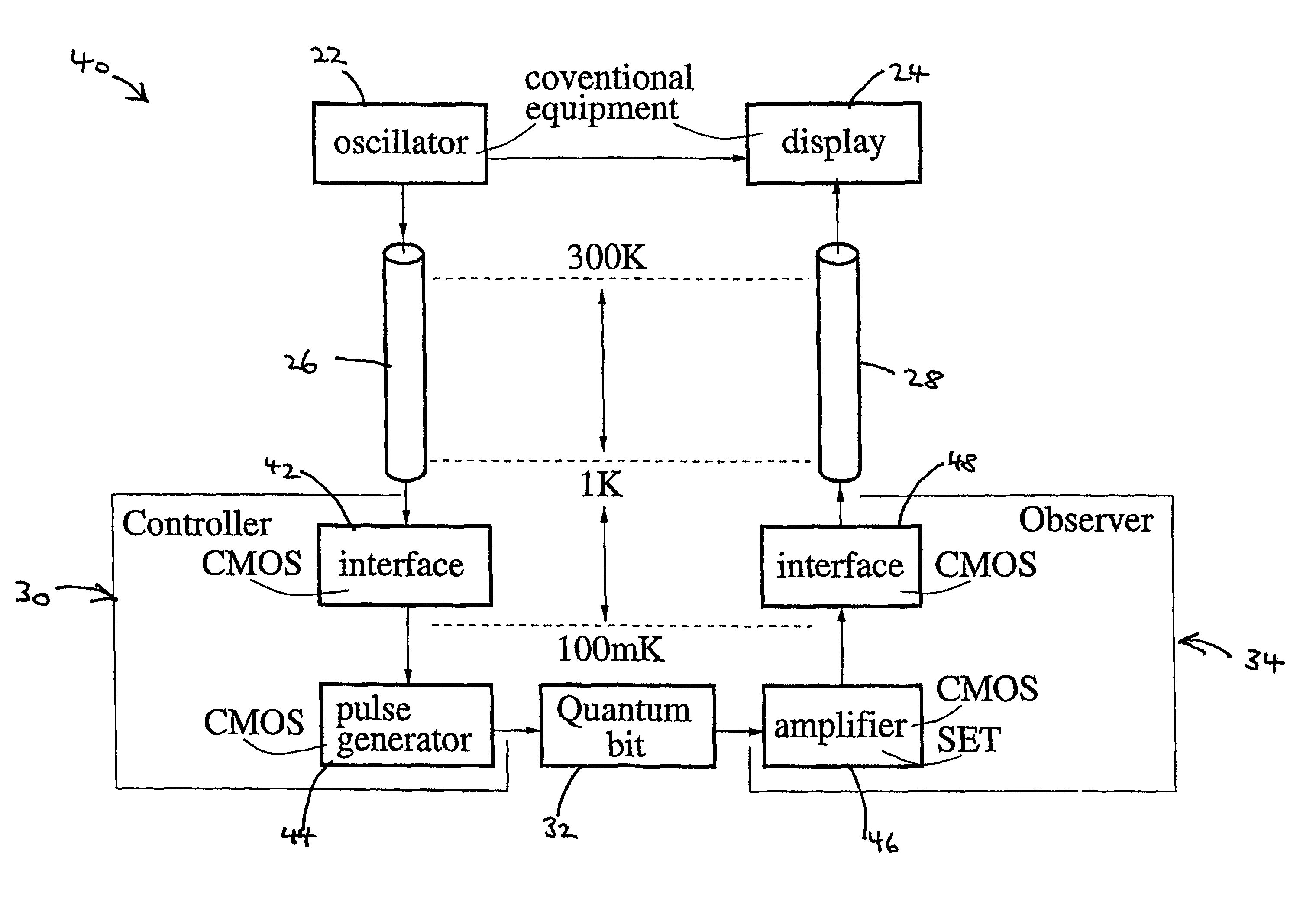
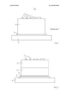
Interfacing at low temperature using CMOS technology
PatentActiveUS7911265B2
Innovation
- The development of ultra-thin silicon-on-insulator (SOI) CMOS technology for fabricating controller and observer circuits, which utilize SOI-CMOSFETs to achieve high unity-gain frequency, rapid pulse edge transition times, high bandwidth, and low power operation, enabling effective control and measurement of quantum bits at low temperatures.
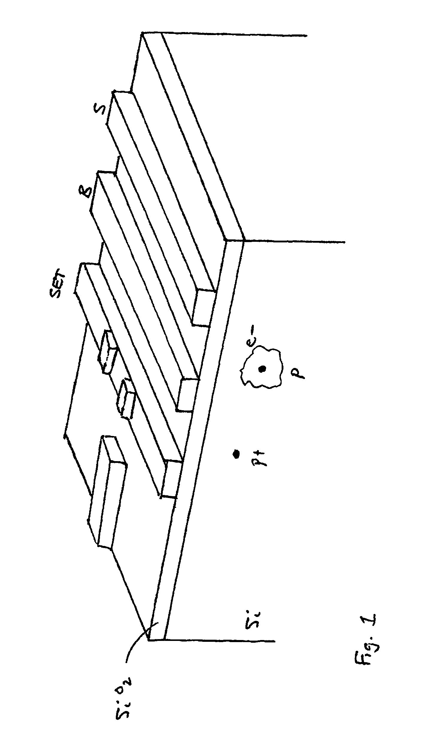
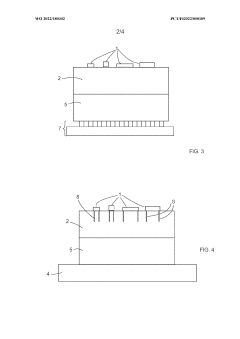
A thermalization arrangement at cryogenic temperatures
PatentWO2022180302A1
Innovation
- A thermalization arrangement with a dielectric substrate and a conductive layer between the substrate and heat sink, where phonons are absorbed by electrons, minimizing thermal boundary resistance and enhancing energy transfer through a conductive joint to an efficient heat sink component, thereby eliminating phonon reflections and improving cooling efficiency.
Quantum Computing Integration with Cryogenic Electronics
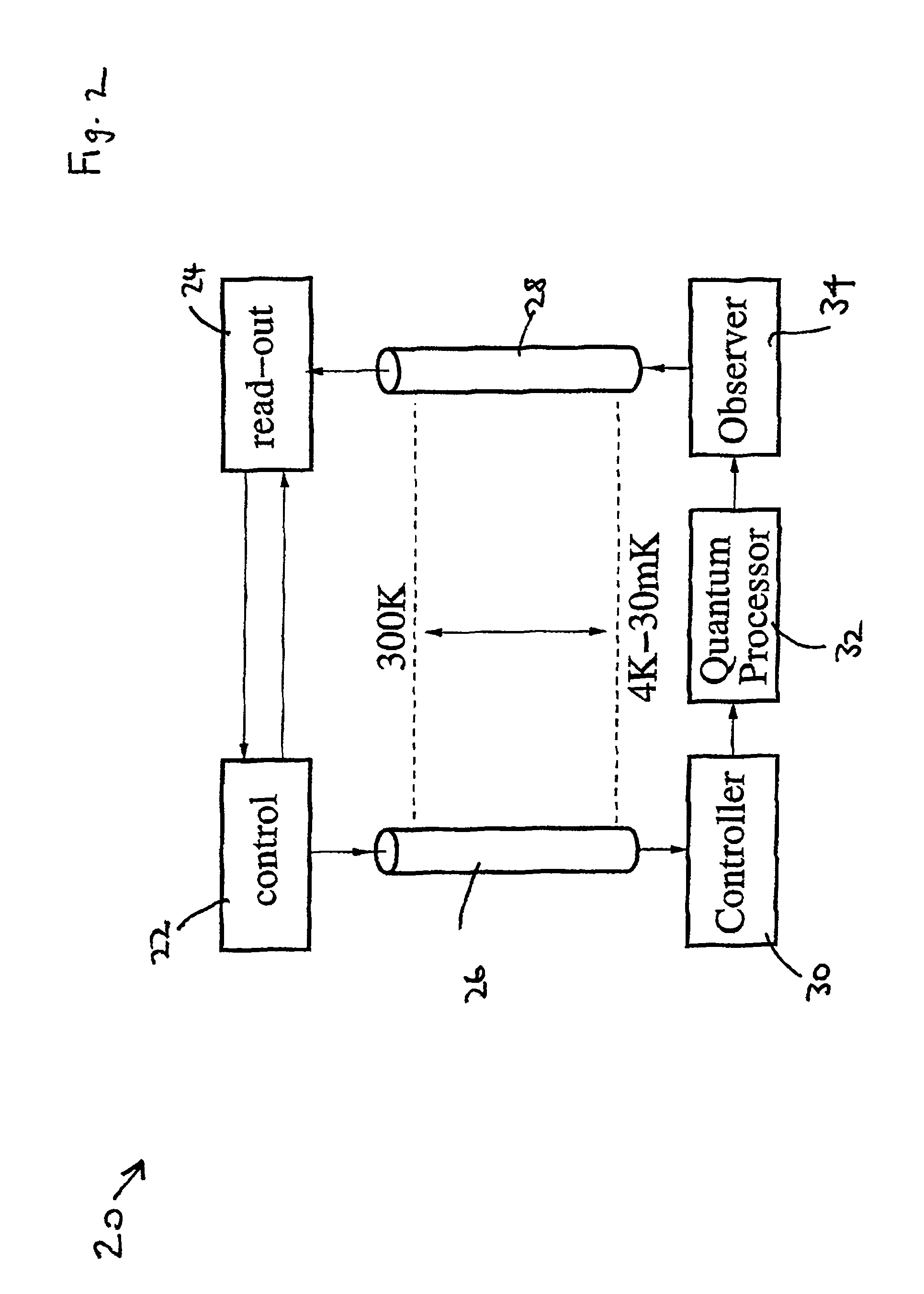
The integration of quantum computing with cryogenic electronics represents a critical frontier in advanced computing technologies. Quantum computers fundamentally require ultra-low temperature environments to maintain quantum coherence and minimize error rates. This necessitates sophisticated cryogenic electronic systems capable of operating efficiently at temperatures approaching absolute zero, typically below 100 mK for superconducting qubits.
Current integration efforts focus on developing control and readout electronics that can function directly within the cryogenic environment. Traditional approaches require room-temperature electronics connected to quantum processors via lengthy cables, introducing latency, heat load, and signal integrity challenges. Moving control electronics closer to quantum processors significantly reduces these issues but demands materials and components engineered specifically for cryogenic performance.
Several semiconductor technologies show promise for cryogenic integration, including silicon CMOS, silicon-germanium BiCMOS, and III-V compound semiconductors. Each offers distinct advantages: CMOS provides density and scalability advantages, SiGe BiCMOS delivers superior high-frequency performance at low temperatures, while III-V semiconductors excel in specific niche applications requiring unique electrical properties.
Superconducting electronics, particularly Single Flux Quantum (SFQ) logic, represent another integration pathway. These circuits leverage superconducting materials like niobium and operate using magnetic flux quanta rather than voltage levels, enabling ultra-high-speed operation with minimal power dissipation—critical for maintaining the cryogenic environment's thermal budget.
The interface between quantum and classical domains presents significant engineering challenges. Researchers are developing specialized cryogenic components including low-noise amplifiers, high-speed data converters, and multiplexing systems to efficiently bridge these domains while minimizing thermal impact on the quantum processor.
Material innovation remains central to advancement, with ongoing research into superconducting interconnects, novel dielectric materials with stable properties at cryogenic temperatures, and packaging solutions that maintain thermal isolation while providing necessary electrical connectivity.
Industry-academia collaborations are accelerating progress, with companies like IBM, Google, and Intel partnering with research institutions to develop integrated cryogenic control systems. These efforts aim to create a complete cryogenic electronics stack that can scale alongside increasing qubit counts, ultimately enabling practical quantum computing systems that deliver on the technology's transformative potential.
Environmental Impact of Cryogenic Cooling Systems
The environmental impact of cryogenic cooling systems used in low-temperature electronics represents a significant consideration in the broader implementation of cryogenic technologies. These systems, essential for maintaining the superconducting properties of materials in cryogenic electronics, consume substantial energy and resources while potentially contributing to various environmental concerns.
Primary cooling methods for cryogenic electronics include liquid helium, liquid nitrogen, and mechanical cryocoolers, each with distinct environmental footprints. Liquid helium, while offering the lowest temperatures necessary for certain superconducting materials, presents particular environmental challenges due to its scarcity as a non-renewable resource. Global helium reserves are limited, and its extraction is energy-intensive, contributing to greenhouse gas emissions.
Liquid nitrogen systems, though operating at higher temperatures than helium-based systems, offer improved environmental performance with lower production energy requirements and greater resource abundance. However, the production process still demands significant energy input and generates carbon emissions, particularly when powered by fossil fuel sources.
Mechanical cryocoolers present an alternative with reduced direct resource consumption but typically require substantial electrical power for operation. The environmental impact of these systems largely depends on the source of electricity, with renewable energy sources significantly reducing their carbon footprint compared to fossil fuel-derived power.
The refrigeration efficiency of cryogenic systems presents another environmental consideration. Traditional cooling technologies often operate at 5-30% of Carnot efficiency, resulting in considerable energy wastage. Recent advancements in pulse tube refrigerators and magnetic cooling technologies have improved efficiency metrics, potentially reducing environmental impact through decreased energy consumption.
Cryogenic system leakage also poses environmental concerns. While nitrogen release has minimal direct environmental impact, helium leakage represents a permanent loss of a finite resource. Additionally, some older cooling systems utilized chlorofluorocarbons (CFCs) or hydrochlorofluorocarbons (HCFCs) with significant ozone depletion potential, though modern systems have largely transitioned to more environmentally benign alternatives.
Life cycle assessment studies indicate that the operational phase dominates the environmental impact of cryogenic cooling systems, accounting for approximately 80-90% of lifetime emissions. This highlights the importance of energy efficiency improvements and clean energy sourcing in reducing environmental footprint. Emerging technologies, including high-temperature superconductors that require less intensive cooling and advanced insulation materials that reduce cooling loads, offer promising pathways toward more environmentally sustainable cryogenic electronics.
Unlock deeper insights with PatSnap Eureka Quick Research — get a full tech report to explore trends and direct your research. Try now!
Generate Your Research Report Instantly with AI Agent
Supercharge your innovation with PatSnap Eureka AI Agent Platform!